Article

The Effect of Deposition Temperature of TiN Thin Film Deposition Using Thermal Atomic Layer Deposition

Vacuum Equipment R&D Division, Semiconductor Research Center, Hanwha Corporation, Pangyo-ro 305, Seongnam 13488, Republic of Korea
*
Author to whom correspondence should be addressed.
Coatings 2023, 13(1), 104; https://doi.org/10.3390/coatings13010104
Submission received: 12 December 2022 / Revised: 2 January 2023 / Accepted: 4 January 2023 / Published: 5 January 2023
(This article belongs to the Special Issue Advanced Films and Coatings Based on Atomic Layer Deposition)

Abstract

:
In this study, the effect of deposition temperature of TiN thin films deposited using the thermal atomic layer deposition (ALD) method was investigated. TiCl4 precursor and NH3 reactive gas were used, and the deposition rate, resistivity change, and surface morphology characteristics were compared in the deposition temperature range of 400 °C–600 °C. While resistivity decreased to 177 µΩcm as the deposition temperature increased to 600 °C, an increase in surface roughness (Rq) to 0.69 nm and a deterioration in the step coverage were identified. In order to obtain a high-quality TiN thin film with excellent resistivity and step coverage characteristics even at low deposition temperatures, the TiN thin film was post-treated with plasma in a combination of N2/He gas ratio of 3:2 to confirm the change in resistivity. X-ray diffraction analysis confirmed crystallization change in the TiN thin film caused by plasma energy. As a result, the resistivity of the TiN thin film deposited at 400 °C was confirmed to be lowered by about 25%.

1. Introduction

Al is one of the materials used in the semiconductor metal wiring process. It has good adhesion to SiO2 and excellent processability. However, when Al and Si come in contact, they tend to mix with each other. As a result, the mating surface may be destroyed during the Al wiring process. To prevent this occurrence, a metal serving as a barrier is deposited between the Al and the Si wafer junction surface. This is called a barrier metal. Thus, the bonding surface can be prevented from being destroyed by forming a double thin film. W also has poor adhesion on the SiO2 surface; as WF6 has high reactivity, a barrier metal is required. For the barrier metal, TiN thin films deposited using physical vapor deposition (PVD) or metalorganic chemical vapor deposition (MOCVD) are mainly used [1]. TiN barrier metal deposited with ALD has recently drawn attention owing to the transition of semiconductor integrated circuits into multilayer wiring structures due to the high integration of semiconductor devices. The TiN thin film, which has excellent material properties, is widely used as a diffusion barrier film in the wiring of Al and Cu because of its low resistivity, high melting point, thermal stability, and good adhesion in very large-scale integration (VLSI) [2,3]. Until now, the CVD method has been actively studied as a deposition method of TiN films. However, there are some problems in applying the commonly used CVD methods to VLSI manufacturing. For example, in order to deposit a TiN thin film using the CVD method in a multilayer wiring process, a high deposition temperature of 600 °C or more is required, which is difficult to apply. On the contrary, when the deposition temperature is 400 °C or less, serious reliability problems occur due to the inclusion of impurities such as Cl in the thin film. TiN thin films are usually deposited by a substitution reaction between TiCl4 (Ti-tetrachloride) and NH3. TiN ALD technology was first studied using TiCl4 (Ti-tetrachloride) and NH3. TiN was deposited by a substitution reaction between TiCl4 and NH3, and this is the most common method of depositing TiN to date. When using halide precursors, such as TiCl4, TiN thin film deposition is possible at various deposition temperatures (300 °C–550 °C). In addition, it has the advantage of lowering production costs due to low manufacturing costs of the precursor. However, halide precursors have the disadvantage of generating by-products with strong corrosiveness [4]. For example, if the reaction chamber is stainless steel or a nitride film is deposited on a copper thin film, hydrochloric acid may be generated. To solve these impurities in the thin film deposition, a metal–organic precursor is used to deposit TiN thin films. Representative materials of metallic organic precursors include TDMAT [Tetrakis(dimethylamido)titanium(IV)], TDEAT [Tetrakis(diethylamido)titanium], and TEMAT [(Tetrakis(ethylmethylamino)titanium] precursor. However, even in this case, the concentration of impurities such as C and O is high due to the bonding structure of the precursor. Because these impurities degrade the performance of the diffusion prevention film, the ALD method, a new TiN deposition film method with excellent step coverage characteristics in trench patterns with a very high aspect ratio and low impurity contamination and resistivity, has been actively studied [5,6,7]. ALD TiN thin film is a material in which thin films with crystalline and amorphous properties grow by changing process factors. Both crystalline thin films and amorphous thin films are reported frequently. When halide-based precursors are used, thin films with crystalline properties are mainly deposited, whereas thin films with amorphous properties are mainly deposited when metal–organic precursors are used. When halide-based precursors and NH3 are used, crystalline thin films are mainly deposited. The ALD method inhibits gas phase reactions between each other by injecting sources and reactants into a time split, leading to limited reactions on the surface. Thus, particle generation is inhibited, and the film is deposited in units of atomic layers regardless of the amount of source. Therefore, when TiN is deposited using the ALD method, it has a large area, a low temperature process, excellent step coverage characteristics, and excellent thickness uniformity characteristics; further, it can prevent the inflow of impurities and particles. In addition, the ALD method can accurately control the chemical composition of the thin film, thereby obtaining a thin film with high purity. Recent studies have been actively conducted to demonstrate 100% conformality in high aspect ratio trench patterns [8]. In this study, TiCl4 precursor and NH3 reactant gas are used to reduce the process temperature and resistivity of TiN thin films deposited by the ALD method and to improve the step coverage characteristics at an aspect ratio of 20:1. In addition, as a method of improving the physical properties of thin film as a diffusion prevention film, we intend to prepare TiN thin film showing excellent properties with reduced resistivity through N2/He plasma treatment.

2. Experiment and Discussion

2.1. Experimental Method

In this study, a wafer obtained by depositing 100 nm of silicon oxide on a 12-inch Si (100) substrate was used to form a TiN thin film using the ALD method. To measure the resistance of the TiN thin film, the bare wafer must be deposited in an insulator where its resistance is unaffected. The TiCl4 precursor was used as the source material, NH3 as the reaction gas, and N2 as the purge gas. The process pressure was 6–7 torr, the deposition temperature was 350 °C–600 °C, and the characteristics were evaluated based on temperature gradient. The TiCl4 precursor is in liquid state at room temperature and has evaporation properties at 5 mmHg and 15 °C. Because a carrier gas was not required in previous studies, it was not used in this study. Table 1 displays the experimental conditions, including each process parameter.
Meanwhile, the plasma treatment was carried out at a chamber temperature of 400 °C by constructing a separate capacitively coupled plasma type chamber. The ratio of N2/He gas was fixed at 3: 2, and a radio frequency (RF) voltage of 13.56 MHz was configured on the upper part of the chamber for plasma formation. The RF matcher applied 700 watts using a 1 kW capacity. Process margin based on matcher capacity and plasma damage caused by RF power were taken into account [9,10]. Plasma treatment conditions and parameters are listed in Table 2.
The properties of the deposited TiN thin film were examined using the following analysis. The thickness of the deposited TiN thin film was calculated by measuring 49 points on a wafer using X-ray fluorescence (XRF). Rigaku’s MFM310 model was used for XRF and MStech’s 4-point probe was used to measure the resistivity of TiN thin film. XRD (model: SmartLab) analysis confirmed the crystallinity of the thin film, and X-ray photoelectron spectroscopy (XPS) (model: K-Alpha+) analysis was performed to determine the degree of contamination of Cl, an impurity in the membrane. Surface analysis based on process variables compared the surface roughness of TiN thin films using atomic force microscopy (AFM) (model: NX20) analysis. To confirm step coverage in the pattern, a TiN thin film was deposited on a wafer formed with a trench of an aspect ratio of 20: 1 and step coverage was observed using transmission electron microscopy (TEM) (model: Tecnai G2 F30 S-Twin) analysis.

2.2. Experimental Results and Discussion

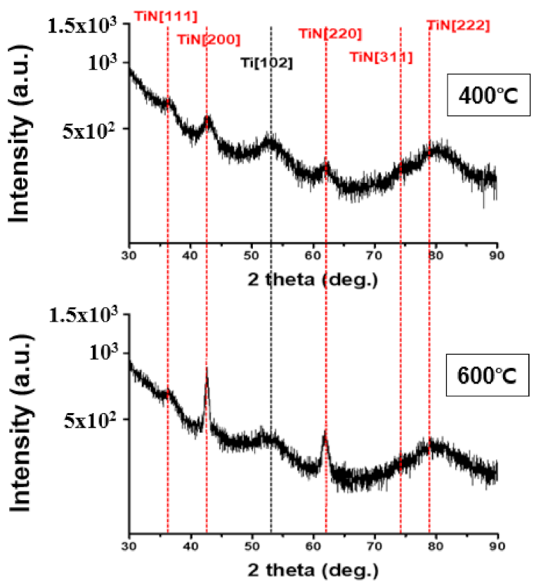
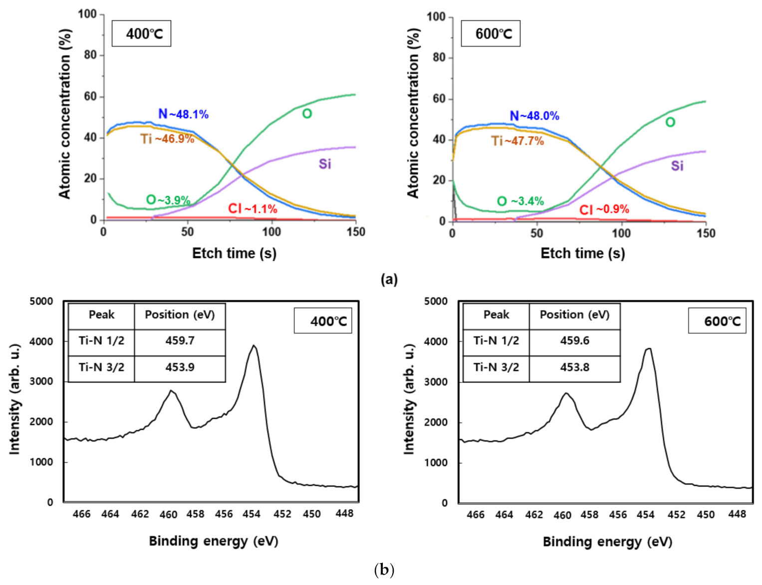
2.2.1. Flat Wafer Characteristic Evaluation

In the ALD process, the formation of a thin film is achieved by repeating the periodic feeding of each reactant and the purging step. It is well known that TiN thin films are formed by chemical interaction when TiCl4 is used as a precursor and NH3 as the reaction gas. When TiCl4 is fed onto the wafer and then purged, only one layer of TiCl4 molecules remains on the wafer owing to the self-limiting reaction, and the molecules that cannot participate in the reaction are pumped out of the chamber. Thereafter, NH3 gas is injected, which breaks the bonds of TiCl4 molecules on the surface, forming a TiN thin film and removing the remaining residues via the N2 purge. The chemical Equations (1) and (2) between TiCl4 precursor and NH3 reaction gas are as follows [11,12]:
TiCl4(g) + 2NH3(g) → TiN(s) + 4HCl(g) + H2 + 1/2N2(g)
6TiCl4 + 8NH3(g) → 6TiN(s) + 24HCl(g) + N2(g)
The deposition temperature is an important process variable for TiN thin films [13]. The substitution reaction between TiCl4 precursor and NH3 reaction gas requires a process temperature sufficient to activate the self-limiting reaction. Generally, the reaction temperature of TiN is 400 °C–500 °C. In this study, to better understand the reaction temperature interval of TiN, the deposition rate based on the deposition temperature at the temperature range of 250 °C–600 °C was examined (Figure 1).
In the temperature range of 250 °C–600 °C, it can be confirmed that the TiN thin film has a tendency to increase the deposition rate as the temperature rises and is deposited normally. In particular, it is confirmed that the temperature rise intervals of 250 °C–400 °C and 550 °C–600 °C are larger than other temperature intervals with regard to deposition rate. Figure 2 shows the change in resistivity based on the deposition temperature. As the temperature increases from 250 °C to 600 °C, the resistivity properties of TiN thin films become distinctly superior. The decrease in resistivity as the deposition temperature increases implies that the electrical properties of the TiN thin film improve as the deposition temperature increases. The resistivity value is affected by membrane impurities, film thickness, microstructure, composition ratio, etc., and the value varies depending on the film formation conditions [14]. Previous studies have shown that the size of the mean grain decreases with the increase in the deposition temperature, and the size of the mean grain increases by about 40% as deposition temperature increases from 400 °C to 550 °C, and resistivity improves [15,16]. Therefore, as the deposition temperature increases, TiN thin films of excellent quality and superior resistivity characteristics can form. Figure 3 shows the change in deposition thickness as the number of deposition cycles of the TiN thin film increases. At 100 cycles, thicknesses of 30.9 Å and 33.1 Å were confirmed under process conditions of 400 °C and 600 °C deposition temperature, respectively. It is confirmed in this graph that TiN thin film thickness and the deposition cycle count have a linear proportional tendency to each other. This means that conventional ALD can produce uniform TiN thin film growth [17,18].
Meanwhile, diffusion prevention films are classified into polycrystalline and amorphous types based on their microstructure. Because there is no grain system used as a diffusion pathway in case of an amorphous anti-membrane, its effect as a diffusion prevention film may be useful. However, as the process temperature increases, crystallization produces a polycrystalline thin film and the grain system serves as a diffusion pathway, while the amorphous anti-membrane has high reactivity and does not meet the conditions for thermal damage and conductivity, making it ineffective as a diffusion prevention film. However, in the case of TiN, which is a crystalline diffusion film, the crystallinity is high, allowing for the formation of dense tissue. Therefore, it has low thermal damage and good adhesion even at high temperatures during the process, making it suitable for use as a diffusion prevention film [19,20]. Figure 4 is the result of XRD analysis performed at deposition temperatures of 400 °C and 600 °C to confirm the crystal structure of TiN thin film. The diffraction peak for the (111) TiN plane at 2θ = 36.6° was shown to be the same in both the temperature bands of 400 °C and 600 °C. A diffraction peak of 2θ = 41.4° was observed for the (200) TiN plane, and a weak peak was observed at 400 °C; however, a strong peak was observed when the deposition temperature was increased to 600 °C. In addition, at 600 °C, the diffraction peak for the (220) TiN plane with 2θ = 61.7° was observed to be stronger than at 400 °C. The reason for this is that as the deposition temperature increases, so does the thermal driving force required to form the TiN thin film [21,22,23]. Peak observations of (111), (200), and (220) in the two deposition temperature intervals indicate that the TiN thin films were formed by polycrystallization. XPS analysis was performed to determine the chemical composition and impurity content. Figure 5a shows the XPS depth profile of TiN thin films deposited at 400 °C and 600 °C. Under both these conditions, the Ti:N ratio in the TiN thin film was confirmed to be ~1:1; thus, Ti and N are expected to form a stoichiometric bond to form a thermally and chemically very safe phase. Figure 5b shows the XPS spectra analysis data of Ti and N. Similar results were measured at 400 °C and 600 °C. The split interval between Ti–N 1/2 and 3/2 peaks was confirmed to be ~5.8 eV, which is similar to the reference split interval of the Ti–nitride bond of 6.0 eV. The content of Cl and O, impurities resulting from TiCl4 precursor and oxide substrates, tends to decrease slightly with increasing deposition temperature. The decrease in Cl content with increasing deposition temperature indicates that the thermal driving force that decomposes the precursor increases as the deposition temperature increases. When the oxide substrate is exposed to the atmosphere for XPS measurement, O is produced because of oxidation on the membrane surface and the thermal diffusion action of the oxide substrate. The decrease in O content from 3.9% to 3.4% as the temperature increased from 400 °C to 600 °C is expected to result in less diffusion movement of elements as the TiN thin film bonds more strongly and crystallizes better at 600 °C.
It is well known that when the grain size of the particles constituting the thin film is small, the morphology of the surface improves. Therefore, increasing the nuclear density can improve surface morphology. The higher the nuclear density, the more that can change into a solid state, resulting in the occurrence of nuclei at multiple locations. In other words, nuclei with different orientations are produced in multiple locations, fresulting in a number of small grains [24]. Nuclear density is heavily influenced by substrate type, pressure, and temperature, and is usually inversely proportional to wafer temperature [25,26]. In this study, AFM analysis was performed to confirm the surface morphology of TiN thin films deposited at 400 °C and 600 °C, as well as the effect of deposition temperature on surface morphology (Figure 6). Rq at 400 °C and 600 °C were 0.41 and 0.69 nm, respectively, indicating that surface roughness increased with increasing temperature. As the deposition temperature increases, the columnar shape develops and the grain size grows, implying that an increase in Rq may also be possible.

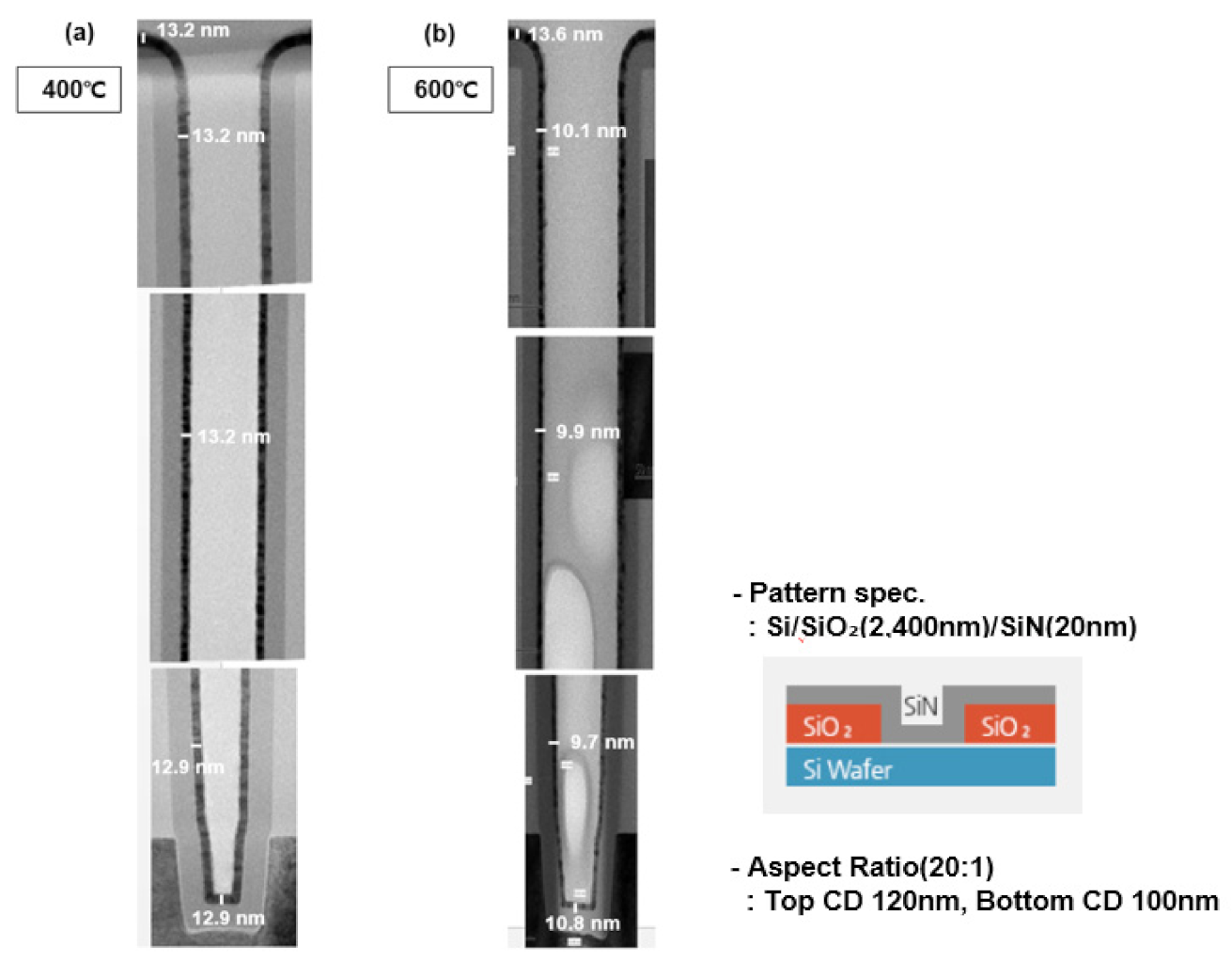
2.2.2. Pattern Wafer Characteristic Evaluation

Figure 7 is a TEM image of a TiN thin film deposited on a bare wafer. Before confirming the step coverage in the pattern, the TEM image of the TiN thin film thickness on the bare wafer and the reliability of the thickness measured were confirmed using an ellipsometer. For the TiN 430 cycle progress and measurement results, the deposition rate measured using an ellipsometer in Figure 3 and the thickness on the TEM image is almost identical.
To measure step coverage in the pattern under the same conditions, a TiN thin film was deposited on a line trench pattern with an aspect ratio of 20: 1 (Figure 8). The depth of the pattern used for step coverage measurement was 2400 nm, with a CD of 120 nm. Step coverage of 98% was confirmed at a deposition temperature of 400 °C and 79% at a deposition temperature of 600 °C. As the deposition temperature increases, the deterioration characteristics of step coverage are confirmed. As the deposition temperature increases, the thermal decomposition is expected to increase, resulting in the deterioration of step coverage. The commonly known pyrolysis temperature of TiCl4 precursor is ~355 °C. The reactivity on the wafer surface increases as the temperature of the wafer increases above that of the precursor pyrolysis [27,28,29,30]. When increasing step coverage at a deposition temperature of 600 °C, it is recommended to set the process conditions in the direction of reducing the amount of source and strengthening the purge.

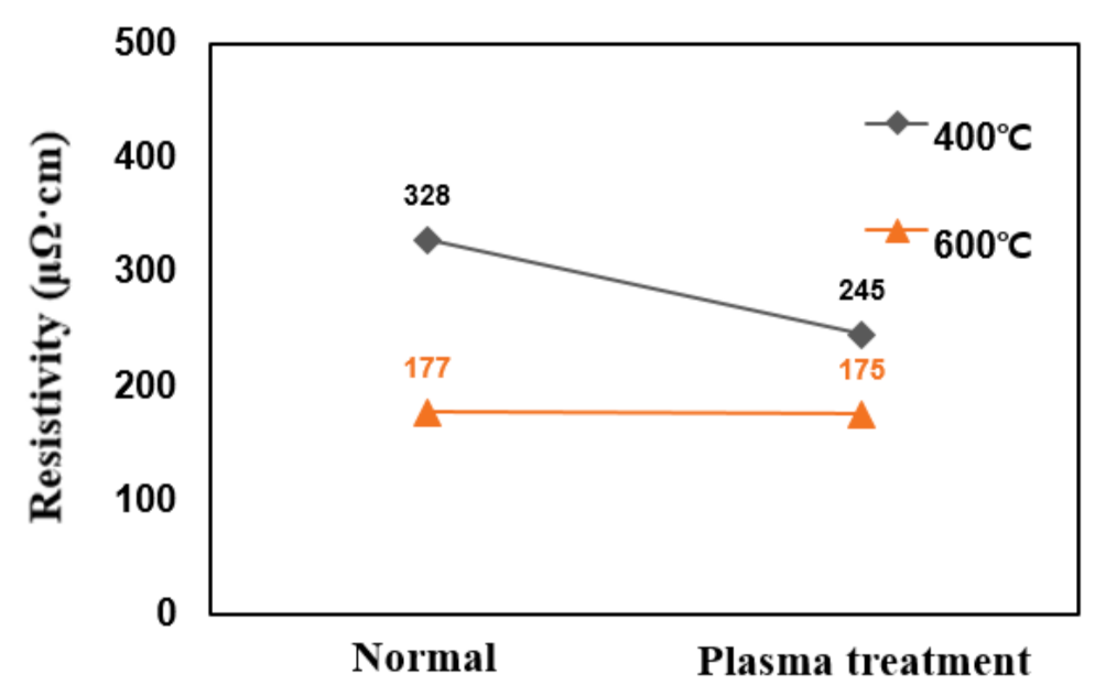
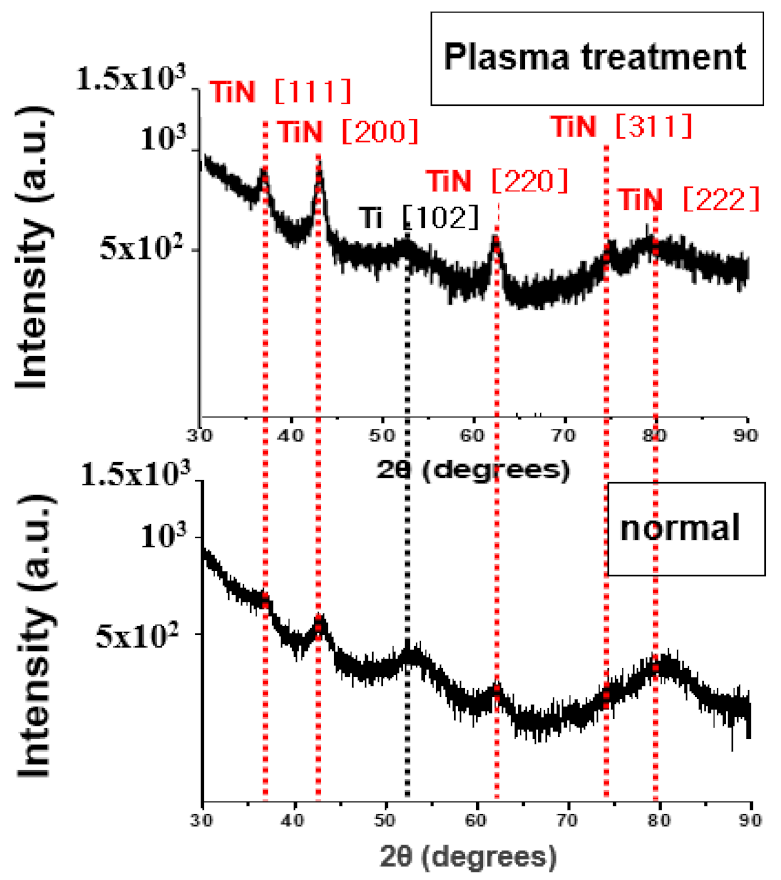
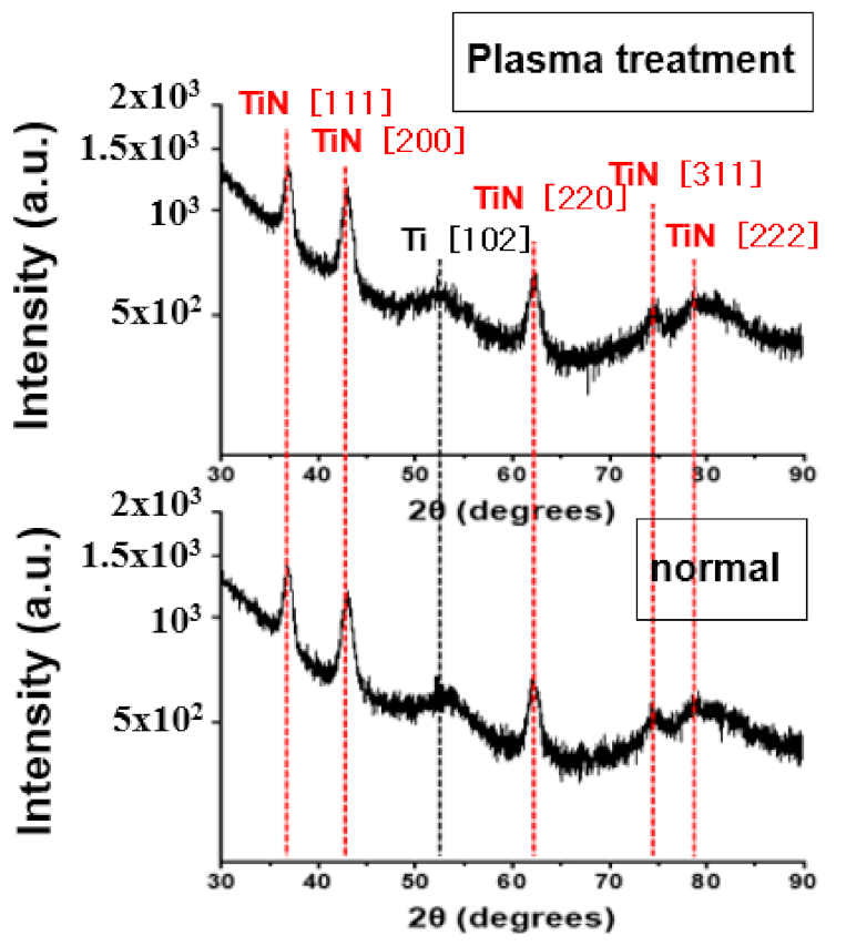
2.2.3. Characterization of Post-Plasma Treatment

In this study, post-plasma treatment of deposited TiN thin films was carried out. Plasma discharge used N2 mixed with He, and the ratio of N2 and He was maintained at 3:2. The addition of gases such as He or Ne to N2 is believed to result in the development of N2-based plasma with increased collective density of reactive species such as atomic nitrogen, nitrogen radicals, or excited nitrogen species. In addition, when plasma is generated from a gas mixture containing nitrogen precursors and additional gases, the pressure in the reaction chamber may be increased more than conventionally used in the plasma-enhanced atomic layer deposition process, further increasing the collective density of reactive species [31,32,33,34,35]. Figure 9 shows the change in resistivity with plasma treatment after TiN thin film deposition. The TiN thin films deposited at deposition temperatures of 400 °C and 600 °C, which was treated with plasma, had resistivity changes of 388–245 µΩcm and 177–175 µΩcm, respectively; thus, this was not very significant.
Crystallization analysis was performed to determine the cause of the decrease in resistivity of plasma treatment at a deposition temperature of 400 °C. Figure 10 is the XRD analysis before and after plasma treatment of TiN thin film deposited at a deposition temperature of 400 °C. The TiN (111), (200), and (220) diffraction peaks can be seen to be more strongly confirmed after the plasma treatment. It can be interpreted that further crystallization of the TiN thin film is achieved by plasma energy.
Figure 11 is the XRD analysis before and after plasma treatment of TiN thin films deposited at a deposition temperature of 600 °C. Unlike the deposition temperature of 400 °C, there was no change in the diffraction peak of 2θ on the XRD data before or after plasma treatment. At 600 °C, the plasma energy has no effect on the crystallinity of the TiN thin film. It can be expected that the TiN thin film deposited at 600 °C has already been sufficiently crystallized by the thermal driving force. The decrease in resistivity because of plasma treatment of TiN thin films deposited at 400 °C is expected to be an effect of increasing the degree of crystallization in TiN thin films.

3. Conclusions

This study examined the difference in the physical properties of TiN thin film deposited using the thermal ALD method based on different deposition temperatures during synthesis. As the deposition temperature increased, the deposition rate increased and the resistivity decreased. The deposition rate per cycle of the TiN thin film at 600 °C was confirmed to be 0.331 Å. The impurity concentration of the TiN thin films deposited at deposition temperatures of 400 °C and 600 °C showed a slight tendency to decrease; however, no significant difference was identified. The surface roughness increased and the step coverage decreased as the deposition temperature increased. When a separate plasma treatment chamber was configured to confirm the effect of post-plasma treatment, it was confirmed that the TiN thin film deposited at 400 °C improved resistivity by about 25% because of the treatment, and it was confirmed that a high-quality TiN thin film with improved electrical properties could be produced even at low temperatures.

Author Contributions

B.-J.L.; Conceptualization, Data curation, Writing—review & editing, Y.-S.K.; Resources, Methodology, D.-W.S.; Formal analysis, Investigation, J.-W.C.; Methodology, Software. All authors have read and agreed to the published version of the manuscript.

Funding

This study was conducted with Hanwha Corporation’s own funding.

Institutional Review Board Statement

Not applicable.

Informed Consent Statement

Not applicable.

Data Availability Statement

Data sharing is not applicable to this article.

Conflicts of Interest

The authors declare no conflict of interest.

References

  1. Elers, K.E.; Winkler, J.; Weeks, K.; Marcus, S. TiCl4 as a Precursor in the TiN Deposition by ALD and PEALD. J. Electrochem. Soc. 2005, 152, G589–G593. [Google Scholar] [CrossRef]
  2. Musschoot, J.; Xie, Q.; Deduytsche, D.; Berghe, S.V.D.; Van Meirhaeghe, R.; Detavernier, C. Atomic layer deposition of titanium nitride from TDMAT precursor. Microelectron. Eng. 2009, 86, 72–77. [Google Scholar] [CrossRef]
  3. De Baynast, H.; Bouteville, A.; Remy, J.-C. Optimization of Titanium Nitride Rapid Thermal CVD Process. Chem. Vap. Depos. 2000, 6, 115–119. [Google Scholar] [CrossRef]
  4. Ansari, M.Z.; Nandi, D.K.; Janicek, P.; Ansari, S.A.; Ramesh, R.; Cheon, T.; Shong, B.; Kim, S.-H. Low-Temperature Atomic Layer Deposition of Highly Conformal Tin Nitride Thin Films for Energy Storage Devices. ACS Appl. Mater. Interfaces 2019, 11, 43608–43621. [Google Scholar] [CrossRef]
  5. Ritala, M.; Leskelä, M.; Rauhala, E.; Haussalo, P. Atomic Layer Epitaxy Growth of TiN Thin Films. J. Electrochem. Soc. 1995, 142, 2731. [Google Scholar] [CrossRef] [Green Version]
  6. Bobb-Semple, D.; Nardi, K.L.; Draeger, N.; Hausmann, D.M.; Bent, S.F. Area-Selective Atomic Layer Deposition Assisted by Self-Assembled Monolayers: A Comparison of Cu, Co, W, and Ru. Chem. Mat. 2019, 31, 1635–1645. [Google Scholar] [CrossRef]
  7. Wojtecki, R.; Mettry, M.; Fine Nathel, N.F.; Friz, A.; De Silva, A.; Arellano, N.; Shobha, H. Fifteen Nanometer Resolved Pat-terns in Selective Area Atomic Layer Deposition-Defectivity Reduction by Monolayer Design. ACS Appl. Mater. Interfaces 2018, 10, 38630–38637. [Google Scholar]
  8. Fenouillet-Beranger, C.; Denorme, S.; Icard, B.; Boeuf, F.; Coignus, J.; Faynot, O.; Brevard, L.; Buj, C.; Soonekindt, C.; Todeschini, J.; et al. Fully-depleted SOI technology using high-k and single-metal gate for 32 nm node LSTP applications fea-turing 0.179 μm2 6T-SRAM bitcell. In Proceedings of the 2007 IEEE International Electron Devices Meeting, Washington, DC, USA, 10–12 December 2007; pp. 267–270. [Google Scholar]
  9. Bekiaris, N.; Wu, Z.; Ren, H.; Naik, M.; Park, J.H.; Lee, M.; Ha, T.H.; Hou, W.; Bakke, J.R.; Gage, M. Cobalt Fill for Advanced Interconnects. In Proceedings of the 2017 IEEE International Interconnect Technology Conference (IITC), Hsinchu, Taiwan, 16–18 May 2017; pp. 1–3. [Google Scholar]
  10. Choi, D.; Barmak, K. On the potential of tungsten as next-generation semiconductor interconnects. Electron. Mater. Lett. 2017, 13, 449–456. [Google Scholar] [CrossRef]
  11. Wen, L.G.; Roussel, P.; Pedreira, O.V.; Briggs, B.; Groven, B.; Dutta, S.; Popovici, M.I.; Heylen, N.; Ciofi, I.; Vanstreels, K.; et al. Atomic Layer Deposition of Ruthenium with TiN Interface for Sub-10 nm Advanced Interconnects beyond Copper. ACS Appl. Mater. Interfaces 2016, 8, 26119–26125. [Google Scholar] [CrossRef]
  12. Hashemi, F.S.M.; Prasittichai, C.; Bent, S.F. A New Resist for Area Selective Atomic and Molecular Layer Deposition on Met-al-Dielectric Patterns. J. Phys. Chem. C 2014, 118, 10957–10962. [Google Scholar] [CrossRef]
  13. Kerrigan, M.M.; Klesko, J.P.; Rupich, S.M.; Dezelah, C.L.; Kanjolia, R.K.; Chabal, Y.J.; Winter, C.H. Substrate selectivity in the low temperature atomic layer deposition of cobalt metal films from bis(1,4-di-tert-butyl-1,3-diazadienyl)cobalt and formic acid. J. Chem. Phys. 2017, 146, 052813. [Google Scholar] [CrossRef]
  14. Chockalingam, M.; Darwish, N.; Le Saux, G.; Gooding, J.J. Importance of the Indium Tin Oxide Substrate on the Quality of Self-Assembled Monolayers Formed from Organophosphonic Acids. Langmuir 2011, 27, 2545–2552. [Google Scholar] [CrossRef]
  15. Seo, S.; Yeo, B.C.; Han, S.S.; Yoon, C.M.; Yang, J.Y.; Yoon, J.; Yoo, C.; Kim, H.-J.; Lee, Y.-B.; Lee, S.J. Reaction Mechanism of Area-Selective Atomic Layer Deposition for Al2O3 Nanopatterns. ACS Appl. Mater. Interfaces 2017, 9, 41607–41617. [Google Scholar] [CrossRef]
  16. Lee, H.J.; Hwang, J.H.; Park, J.Y.; Lee, S.W. Alternative Surface Reaction Route in the Atomic Layer Deposition of Titanium Nitride Thin Films for Electrode Applications. ACS Appl. Electron. Mater. 2021, 3, 999–1005. [Google Scholar] [CrossRef]
  17. Burke, M.; Blake, A.; Povey, I.; Schmidt, M.; Petkov, N.; Carolan, P.; Quinn, A.J. Low sheet resistance titanium nitride films by low-temperature plasma-enhanced atomic layer deposition using design of experiments methodology. J. Vac. Sci. Technol. A Vac. Surf. Film. 2014, 32, 031506. [Google Scholar] [CrossRef]
  18. Snyder, M.Q.; McCool, B.A.; DiCarlo, J.; Tripp, C.P.; DeSisto, W.J. An infrared study of the surface chemistry of titanium nitride atomic layer deposition on silica from TiCl4 and NH3. Thin Solid Film. 2006, 514, 97–102. [Google Scholar] [CrossRef]
  19. Mochizuki, Y.; Okamoto, Y.; Ishitani, A.; Hirose, K.; Takada, T.T.T. On the Reaction Scheme for Ti/TiN Chemical Vapor Deposition (CVD) Process Using TiCl4. Jpn. J. Appl. Phys. 1995, 34, L326. [Google Scholar] [CrossRef]
  20. Zhao, C.; Xiang, J. Atomic Layer Deposition (ALD) of Metal Gates for CMOS. Appl. Sci. 2019, 9, 2388. [Google Scholar] [CrossRef] [Green Version]
  21. Krylov, I.; Qi, Y.; Korchnoy, V.; Weinfeld, K.; Eizenberg, M.; Yalon, E. Role of temperature on structure and electrical properties of titanium nitride films grown by low pressure plasma enhanced atomic layer deposition. J. Vac. Sci. Technol. A 2020, 38, 032403. [Google Scholar] [CrossRef]
  22. Kukli, K.; Ritala, M.; Leskelä, M. Atomic Layer Deposition and Chemical Vapor Deposition of Tantalum Oxide by Successive and Simultaneous Pulsing of Tantalum Ethoxide and Tantalum Chloride. Chem. Mater. 2000, 12, 1914–1920. [Google Scholar] [CrossRef]
  23. Kim, S.K.; Lee, S.W.; Han, J.H.; Lee, B.; Han, S.; Hwang, C.S. Capacitors with an Equivalent Oxide Thickness of <0.5 nm for Nanoelectronic Semiconductor Memory. ECS Meet. Abstr. 2010, MA2010-02, 1414. [Google Scholar] [CrossRef]
  24. Elam, J.W.; Routkevitch, D.; Mardilovich, P.P.; George, S.M. Conformal Coating on Ultrahigh-Aspect-Ratio Nanopores of Anodic Alumina by Atomic Layer Deposition. Chem. Mater. 2003, 15, 3507–3517. [Google Scholar] [CrossRef]
  25. Lee, S.W.; Han, J.H.; Han, S.; Lee, W.; Jang, J.H.; Seo, M.; Kim, S.K.; Dussarrat, C.; Gatineau, J.; Min, Y.-S.; et al. Atomic Layer Deposition of SrTiO3 Thin Films with Highly Enhanced Growth Rate for Ultrahigh Density Capacitors. Chem. Mater. 2011, 23, 2227–2236. [Google Scholar] [CrossRef]
  26. Park, Y.H.; Kim, M.H.; Bin Kim, S.; Jung, H.J.; Chae, K.; Ahn, Y.H.; Park, J.-Y.; Rotermund, F.; Lee, S.W. Enhanced Nucleation of High-k Dielectrics on Graphene by Atomic Layer Deposition. Chem. Mater. 2016, 28, 7268–7275. [Google Scholar] [CrossRef]
  27. Song, S.J.; Park, T.; Yoon, K.J.; Yoon, J.H.; Kwon, D.E.; Noh, W.; Lansalot-Matras, C.; Gatineau, S.; Lee, H.K.; Gautam, S.; et al. Comparison of the Atomic Layer Deposition of Tantalum Oxide Thin Films Using Ta(NtBu)(NEt2)3 and Ta(NtBu)(NEt2)2Cp and H2O. ACS Appl. Mater. Interfaces 2017, 9, 537. [Google Scholar] [CrossRef]
  28. Kim, S.H.; Lee, W.; An, C.H.; Kwon, D.S.; Kim, D.-G.; Cha, S.H.; Hwang, C.S. Effect of Growth Temperature During the Atomic Layer Deposition of the SrTiO3 Seed Layer on the Properties of RuO2/ SrTiO3/Ru Capacitors for Dynamic Random Access Memory Applications. ACS Appl. Mater. Interfaces 2018, 10, 41544. [Google Scholar] [CrossRef]
  29. Van Bui, H.; Groenland, A.W.; Aarnink, A.A.I.; Wolters, R.A.M.; Schmitz, J.; Kovalgin, A.Y. Growth Kinetics and Oxidation Mechanism of ALD TiN Thin Films Monitored by In Situ Spectroscopic Ellipsometry. J. Electrochem. Soc. 2011, 158, H214–H220. [Google Scholar] [CrossRef]
  30. Langereis, E.; Heil, S.B.S.; van Sanden, M.C.M.; Kessels, W.M.M. In situ spectroscopic ellipsometry study on the growth of ultrathin TiN films by plasma-assisted atomic layer deposition. J. Appl. Phys. 2006, 100, 023534. [Google Scholar] [CrossRef] [Green Version]
  31. Tiznado, H.; Zaera, F. Surface Chemistry in the Atomic Layer Deposition of TiN Films from TiCl4 and Ammonia. J. Phys. Chem. B 2006, 110, 13491–13498. [Google Scholar] [CrossRef]
  32. Cheng, H.-E.; Lee, W.-J. Properties of TiN films grown by atomic-layer chemical vapor deposition with a modified gaseous-pulse sequence. Mater. Chem. Phys. 2006, 97, 315–320. [Google Scholar] [CrossRef]
  33. Luoh, T.; Huang, Y.-K.; Hung, Y.-T.; Yang, L.-W.; Yang, T.-H.; Chen, K.-C. TiCl4 Barrier Process Engineering in Semiconductor Manufacturing. Coatings 2016, 6, 2. [Google Scholar] [CrossRef]
  34. Zhao, R.; Wang, X. Initial Growth and Agglomeration during Atomic Layer Deposition of Nickel Sulfide. Chem. Mater. 2019, 31, 445–453. [Google Scholar] [CrossRef]
  35. O’Conner, É.; Brennan, B.; Djara, V.; Cherkaoui, K.; Monaghan, S.; Newcomb, S.B.; Contreras, R.; Milojevic, M.; Hughes, G.; Pemble, M.E.; et al. A systematic study of (NH4)2S passivation (22%, 10%, 5%, or 1%) on the interface properties of the Al2O3/In0.53Ga0.47As/InP system for n-type and p-type In0.53Ga0.47As epitaxial layers. J. Appl. Phys. 2011, 109, 024101. [Google Scholar]
Figure 1. Comparison of deposition rates of TiN thin films per cycle over process temperature.
Coatings 13 00104 g001
Figure 2. Comparison of resistive properties of TiN thin films over process temperature.
Coatings 13 00104 g002
Figure 3. The tendency of deposition thickness as the number of deposition cycles increases.
Coatings 13 00104 g003
Figure 4. XRD analysis to determine the crystal structure of TiN thin films based on deposition temperature.
Coatings 13 00104 g004
Figure 5. XPS analysis according to the deposition temperature change of TiN thin film: (a) depth profile, (b) spectra.
Coatings 13 00104 g005
Figure 6. AFM analysis to determine surface roughness of TiN thin films based on deposition temperature: (a) 400 °C, (b) 600 °C.
Coatings 13 00104 g006
Figure 7. TEM cross-sectional profiles: (a) 400 °C, (b) 600 °C.
Coatings 13 00104 g007
Figure 8. Step coverage characteristics in patterns based on deposition temperature: (a) 400 °C, (b) 600 °C.
Coatings 13 00104 g008
Figure 9. Resistivity changes due to post-plasma treatment after deposition.
Coatings 13 00104 g009
Figure 10. XRD images before and after plasma treatment of TiN thin films deposited at a deposition temperature of 400 °C.
Coatings 13 00104 g010
Figure 11. XRD images of plasma treatment of TiN thin films deposited at a deposition temperature of 600 °C.
Coatings 13 00104 g011
Table 1. Experimental conditions for deposition.
ParameterCondition
PrecursorTiCl4
Reactant gasNH3
Purge gasN2
Pressure6–7 torr
Substrate12 inch Si(100)/oxide (1000 A) wafer
Process temperature350–600 °C
Table 2. Experimental conditions for plasma treatment.
ParameterCondition
Frequency13.56 MHz
RF power700 w (60 s)
Plasma discharge gasN2 (3000 sccm)/He (2000 sccm)
Pressure1 torr
Temperature400 C
Disclaimer/Publisher’s Note: The statements, opinions and data contained in all publications are solely those of the individual author(s) and contributor(s) and not of MDPI and/or the editor(s). MDPI and/or the editor(s) disclaim responsibility for any injury to people or property resulting from any ideas, methods, instructions or products referred to in the content.

