Article

Rear Earth Oxide Multilayer Deposited by Plasma Spray-Physical Vapor Deposition for Envisaged Application as Thermal/Environmental Barrier Coating

1
Chengdu Holy (Group) Industry Co., Ltd., Chengdu 610041, China
2
National Engineering Laboratory for Modern Materials Surface Engineering Technology & The Key Lab of Guangdong for Modern Surface Engineering Technology, Institute of New Materials, Guangdong Academy of Science, Guangzhou 510650, China
3
Guangxi Key Laboratory of Automobile Components and Vehicle Technology, Guangxi University of Science & Technology, Liuzhou 545006, China
4
School of Materials and Energy, Guangdong University of Technology, Guangzhou 510006, China
*
Author to whom correspondence should be addressed.
Coatings 2021, 11(8), 889; https://doi.org/10.3390/coatings11080889
Submission received: 26 June 2021 / Revised: 17 July 2021 / Accepted: 21 July 2021 / Published: 26 July 2021
(This article belongs to the Special Issue Defects, Stresses and Cracks in Thermal Barrier Coatings)

Abstract

:
SiC fiber-reinforced SiC ceramic matrix composites (SiCf/SiC CMCs) are being increasingly used in the hot sections of gas turbines because of their light weight and mechanical properties at high temperatures. The objective of this investigation was the development of a thermal/environmental barrier coating (T/EBC) composite coating system consisting of an environmental barrier coating (EBC) to protect the ceramic matrix composites from chemical attack and a thermal barrier coating (TBC) that insulates and reduces the ceramic matrix composites substrate temperature for increased lifetime. In this paper, a plasma spray-physical vapor deposition (PS-PVD) method was used to prepare multilayer Si–HfO2/Yb2Si2O7/Yb2SiO5/Gd2Zr2O7 composite coatings on the surface of SiCf/SiC ceramic matrix composites. The purpose of this study is to develop a coating with resistance to high temperatures and chemical attack. Different process parameters are adopted, and their influence on the microstructure characteristics of the coating is discussed. The water quenching thermal cycle of the coating at high temperatures was tested. The results show that the structure of the thermal/environmental barrier composite coating changes after water quenching because point defects and dislocations appear in the Gd2Zr2O7 and Yb2SiO5 coatings. A phase transition was found to occur in the Yb2SiO5 and Yb2Si2O7 coatings. The failure mechanism of the T/EBC composite coating is mainly spalling when the top layer penetrates cracks and cracking occurs in the interface of the Si–HfO2/Yb2Si2O7 coating.

1. Introduction

With the development of aero-engines, the performance requirements for high-temperature-resistant hot-end components to resist high-temperature environmental corrosion have further increased. Due to their low density, resistance to high temperatures (up to 1650 °C), and excellent resistance to chemical attack, SiC fiber-reinforced SiC ceramic matrix composites (SiCf/SiC CMCs) have become the most promising materials in the field of new-generation aero-engines. However, SiCf/SiC CMC substrates are subject to rapid corrosion failure when used in aero-engines under harsh conditions such as high temperature, high pressure, and exposure to multiple molten salts. To solve this problem, thermal/environmental barrier coatings (T/EBCs) are applied to the surface of SiCf/SiC CMC to improve the resistance of hot-end components to high temperatures and corrosion [1,2].
The SiC fiber-reinforced SiC ceramic matrix composites’ substrate materials are effectively isolated from high-temperature corrosive environments by T/EBCs, which greatly reduces high-temperature corrosion of the materials by the environment and prolongs the service life of components. A new generation for T/EBC coatings contains Si/Mullite+BSAS/Rare-Earth (RE) silicates, which can tolerate service temperatures that exceed 1400 °C [3]. The thermal conductivity of Gd2Zr2O7-type TBCs is considerably lower than that of 8YSZ-type TBCs, leading to their widespread application in the thermal insulation and protection of aero-engine blades [4,5]. A Yb2Si2O7–Yb2SiO5 composite coating has thermomechanical stability and a high-temperature crack self-repair capability [6,7,8]. An Si–HfO2 coating is intended to provide a well-bonded interface between the EBC ceramic layer and the CMC substrate, and the addition of HfO2 provides better mechanical properties at higher temperatures [9].
In this paper, a plasma spray-physical vapor deposition (PS-PVD) method is used to prepare multilayer Si–HfO2/Yb2Si2O7/Yb2SiO5/Gd2Zr2O7 T/EBC composite coatings on the surface of SiC fiber-reinforced SiC ceramic matrix composites substrates. The blades of gas turbines need EBC to protect them from corrosion in high-temperature corrosive environments, while TBC acts as thermal insulation to make them work at higher temperatures. Different process parameters are adopted, and their influence on the microstructure characteristics of the coating is discussed. To explore the failure mechanism of the coating under the service condition of a thermal cycle, the water quenching thermal cycle of the coating at high temperatures was tested. This research on new thermal environment barrier coatings in this paper will provide fundamental data and technical support for advanced civil aviation engine airworthiness.

2. Experimental

2.1. Coating Preparation

In this experiment, a PS-PVD multilayer system (Sulzer-Metco, Winterthur, Switzerland) was used for spraying experiments on a SiCf/SiC CMC substrate. Each layer of powder was uniformly coated on the surface of the SiCf/SiC CMC material by a spray gun (O3CP plasma gun). First, the pretreatment process was performed on the SiCf/SiC CMC material. The SiCf/SiC CMC material of rectangular (25 × 4.5 × 4 mm3) was blasted with Al2O3 particles at 0.4 MPa (10 times). After sandblasting, the SiCf/SiC CMC substrates were placed in acetone and ultrasonically cleaned for 10 min. The composite material was placed in the PS-PVD instrument after cleaning for coating by the spray treatment. Each layer of powder (Si-10%HfO2, Yb2Si2O7, Yb2SiO5, and Gd2Zr2O7) was sprayed on the SiCf/SiC CMC substrate in sequence. The spraying parameters are shown in Table 1. A schematic diagram of the finished T/EBC coating is shown in Figure 1a. The microscopic morphology of the sprayed powder in each coating is shown in Figure 1b–e. Figure 1b shows the morphology of the top layer, Gd2Zr2O7, with particle sizes between 0.5–2 μm and irregular rhombus shape. Figure 1c shows the morphology of the middle layer, Yb2SiO5 with particle sizes in the 2–4 μm range, and irregular polygonal shapes like the Gd2Zr2O7 powder. However, the overall sizes of the Yb2SiO5 particles are twice that of the Gd2Zr2O7 particles. Figure 1d shows the morphology of the middle layer, Yb2Si2O7. After pretreatment and granulation, the Yb2Si2O7 powders were spherical particles with sizes of approximately 13 μm. The special spherical shape provides the excellent fluidity of the powder, which is conducive to its uniform flow in the spray gun [10,11]. Figure 1e shows the morphology of Si powder containing 10% HfO2, with a particle diameter of approximately 40 μm. Similar to the Gd2Zr2O7 and Yb2SiO5 powders, they are irregular polygons. However, the particle size of Si powder containing 10% HfO2 is 10 and 5 times larger than Gd2Zr2O7 and Yb2SiO5 powders, respectively.

2.2. Thermal Thermal Shock Test

Samples were subjected to a water quenching test to determine the thermal cycle performance of the T/EBC coating. The thermal cycle was divided into three stages: heating, heat preservation, and cooling. The thermal cycles consisted of 5-min heat up, 10-min dwell at 1300 °C, and water quenching for 5 min to room temperature. After 10 water quenching cycles, the microstructure of the cross-section of the sample was characterized.

2.3. Characterization

X-ray diffraction (XRD, D8-ADVANCE, Bruker, Hanau, Germany, Cu) analysis was performed with a radiation angle of 10°–90°, a tube voltage of 40 kV, a tube current of 40 mA, and a step length of 0.01° on the coating surface, layer by layer, to observe T/EBC surface phase formation. Field emission scanning electron microscopy (FE-SEM, ZEISS, Tholey, Germany) was used to characterize the morphology, and energy dispersive X-ray spectroscopy (EDS) was performed on the samples. To conduct an in-depth study of the cross-section of the sprayed sample, a focused ion beam (FIB, SMI3050MS2, SII, Tokyo, Japan) was used to strip the interfacial area of each coating for analysis. Transmission electron microscopy (TEM, FEI, Hillsboro, OR, USA) was used to further observe the microscopic area of the T/EBC coating. The interfacial phase was identified by selected area electron diffraction (SAED).

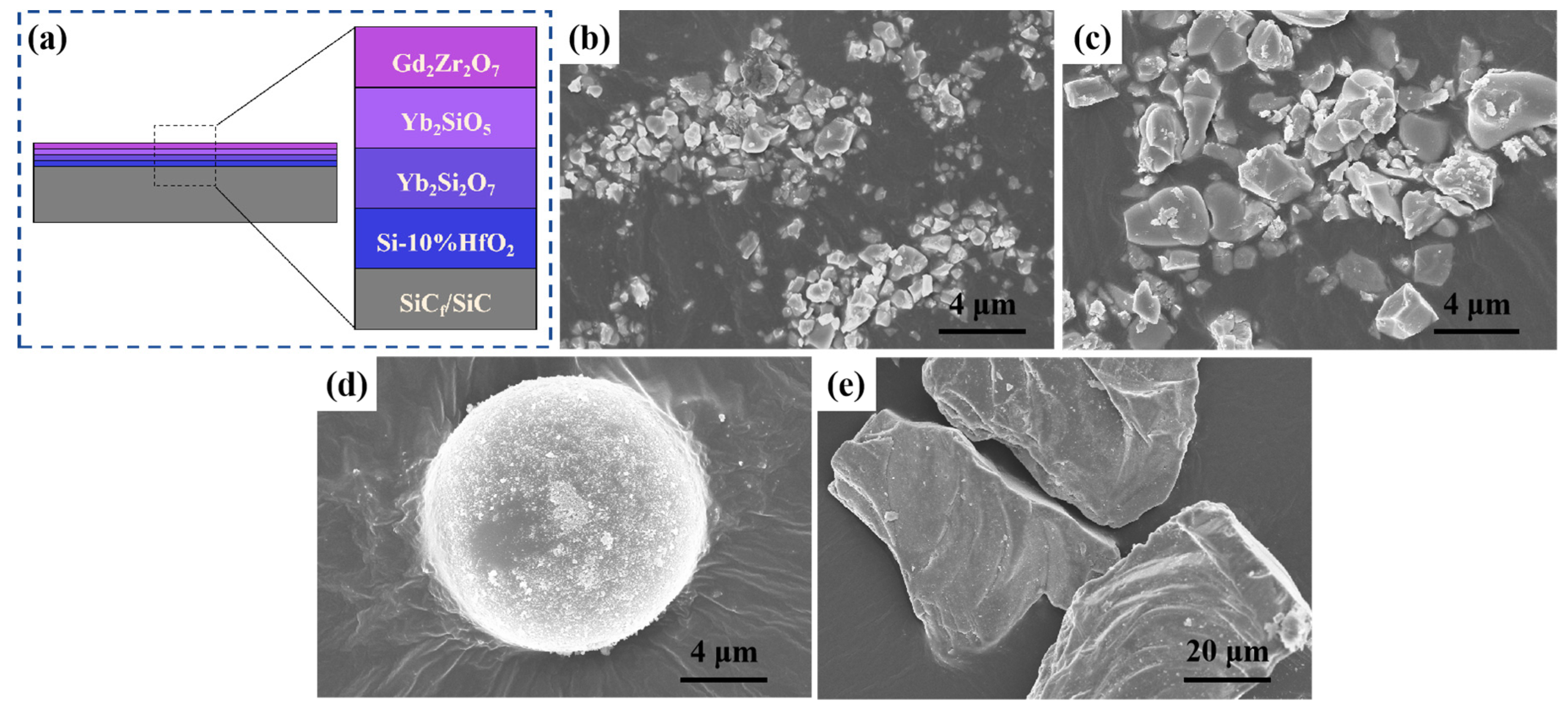
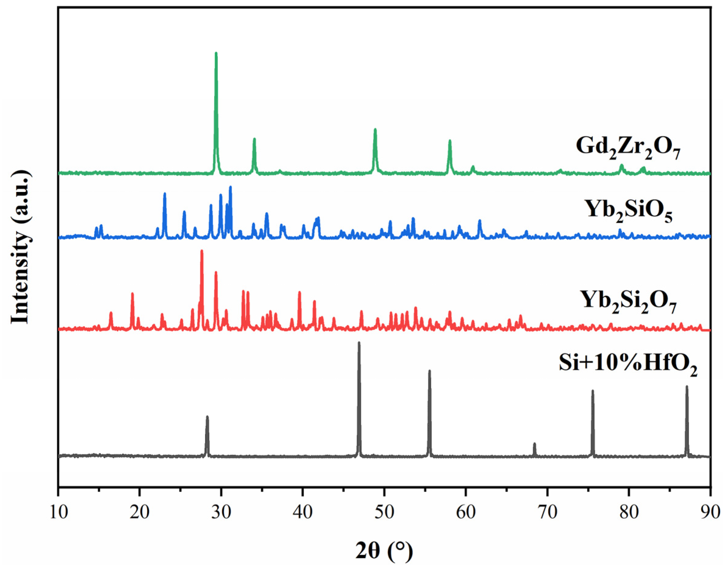
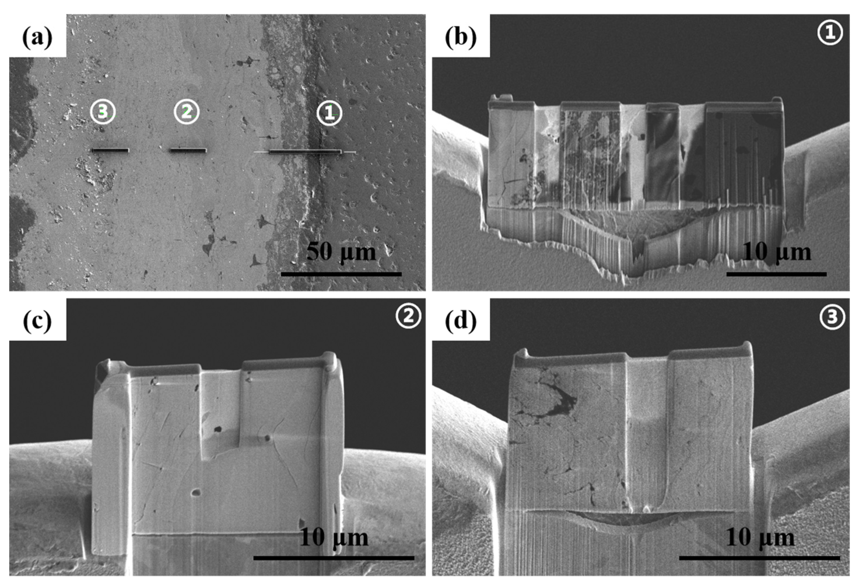
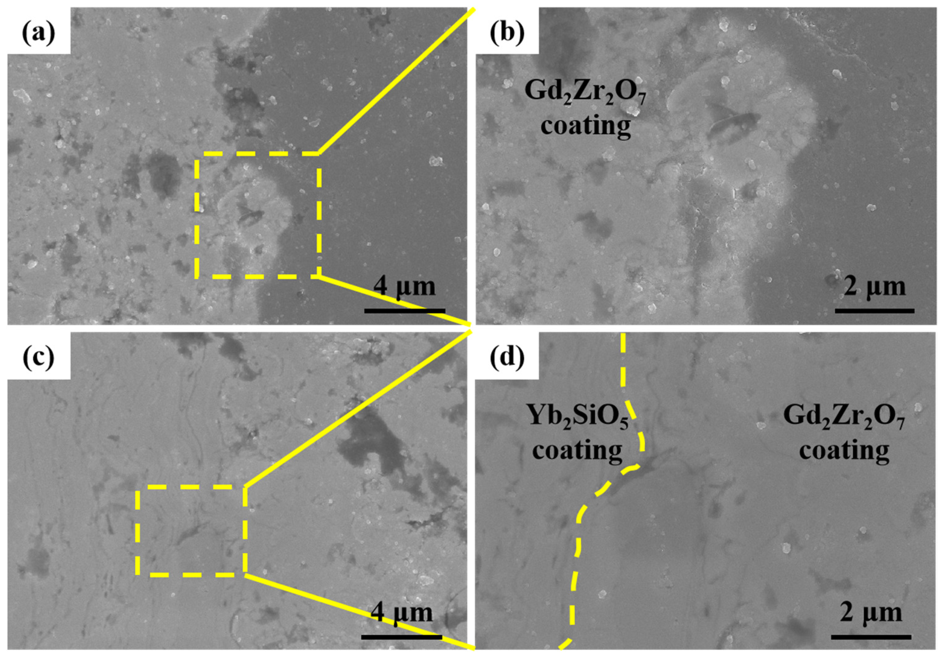
3. Results and Discussion

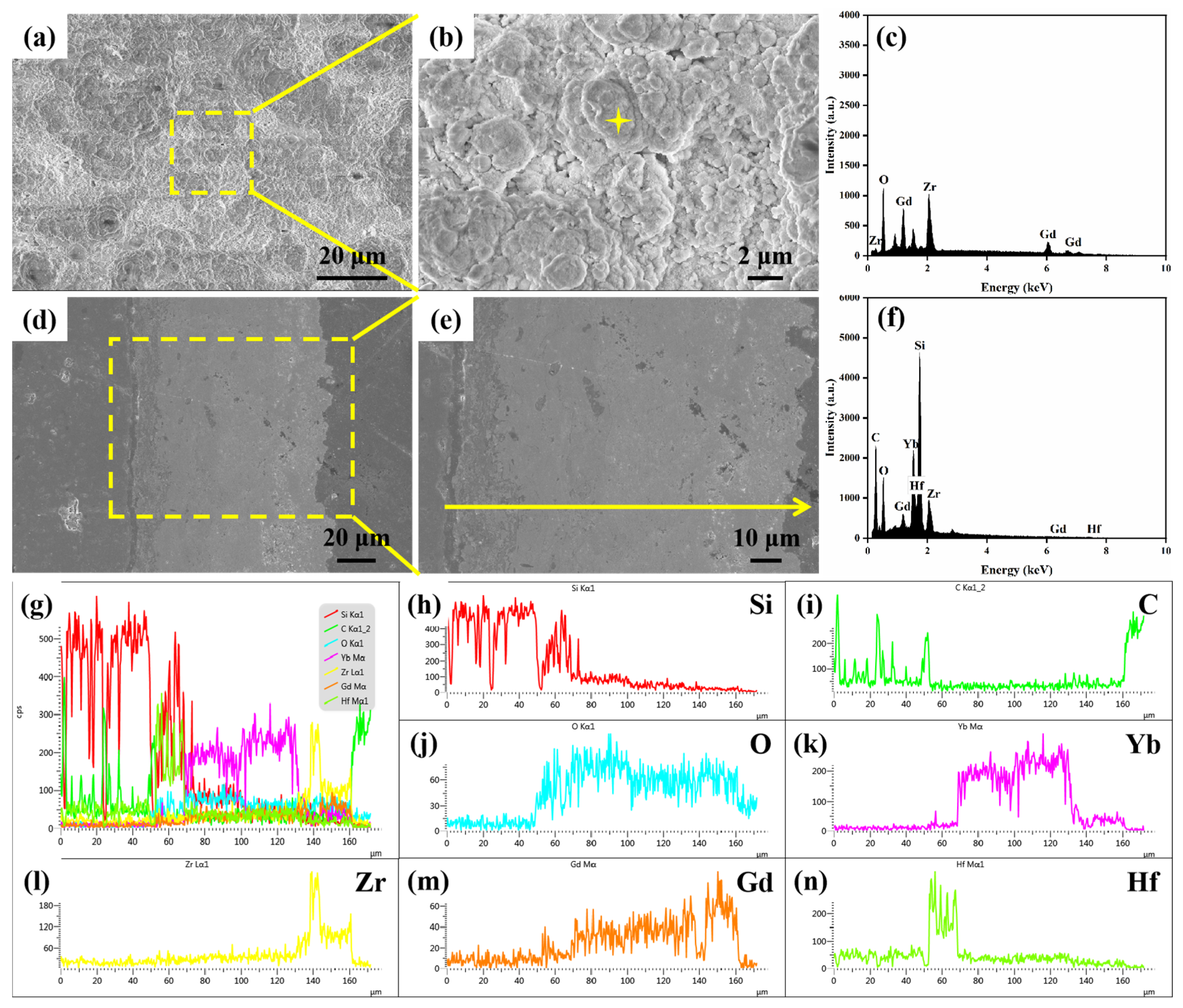
3.1. Microstructure of the As-Sprayed T/EBCs

Using the experimental parameters in Table 1, the composite T/EBC coatings were sprayed on the surface of the SiCf/SiC CMC by a PS-PVD method. The microstructure, composition, and elemental distribution of the T/EBC coatings are presented in Figure 2a–n. Figure 2a,b shows the micromorphology of the surface of the T/EBC coating, and an enlarged view of the microtopography of the coating surface is shown in Figure 2b. Due to the accumulation of molten powder on the surface during the spraying process, the coating surface in Figure 2b is not flat. With more porosity and holes, its surface morphology resembles the appearance of cauliflower. The EDS results for the point in Figure 2b is displayed in Figure 2c. The surface of the top layer contains only the elements O, Gd, and Zr, showing that the surface of the Gd2Zr2O7 layer is not contaminated by other impurities. Figure 2d is the microtopography image of the cross section with T/EBCs. The cross section is smooth without cracks and pits. Figure 2e is an enlarged image of Figure 2d. The line scan result in Figure 2f shows that the cross section contains C, O, Gd, Yb, Hf, Si, and Zr, and no other impurities. Figure 2g is the general diagram of the distribution of all the elements in the coating, and Figure 2h–n is the distribution diagram of each element. Figure 2h,i shows that the Si and C contents are highest on the left side of the line scan, indicating that the base layer SiC is on the left side (Figure 2e). Figure 2h,n shows that the coating close to the base layer, SiC, has the highest content of Si and Hf, indicating that the first layer is Si–HfO2. Figure 2k shows two intermediate layers containing Yb. However, it can be seen from Figure 2h,j that the Si and O contents are higher in the coating next to the Si–HfO2 layer, which indicates that the second layer is Yb2Si2O7. The third layer with less Si and O is Yb2SiO5. From Figure 2l,m, the contents of Gd and Zr are highest in the fourth layer, indicating that the top layer is Gd2Zr2O7.
To further investigate the phase characteristics of each coating after PS-PVD spraying, the phase structure of the coating was analyzed by X-ray diffraction. Whenever the substrate is sprayed with a new coating, small angle X-ray scattering is used for interlayer phase analysis. The XRD pattern of each coating in the T/EBCS coatings is shown in Figure 3. The positions of the diffraction peaks of each coating are consistent with the characteristic peak positions of the Gd2Zr2O7 [12], Yb2SiO5 [13], Yb2Si2O7 [14], and Si–HfO2 [15] coatings, indicating that the coatings combined via physical stacking.
Figure 4a shows an interfacial image of the as-sprayed T/EBC coating milled by FIB. The samples in Figure 4b–d are taken from positions 1, 2, and 3 in Figure 4a. Figure 4b shows that position 1 is the boundary of the Si–HfO2/Yb2Si2O7 coating interface, position 2 is the boundary of the Yb2Si2O7/Yb2SiO5 coating interface (Figure 4c), and position 3 is the boundary of the Yb2SiO5/Gd2Zr2O7 coating interface (Figure 4d).

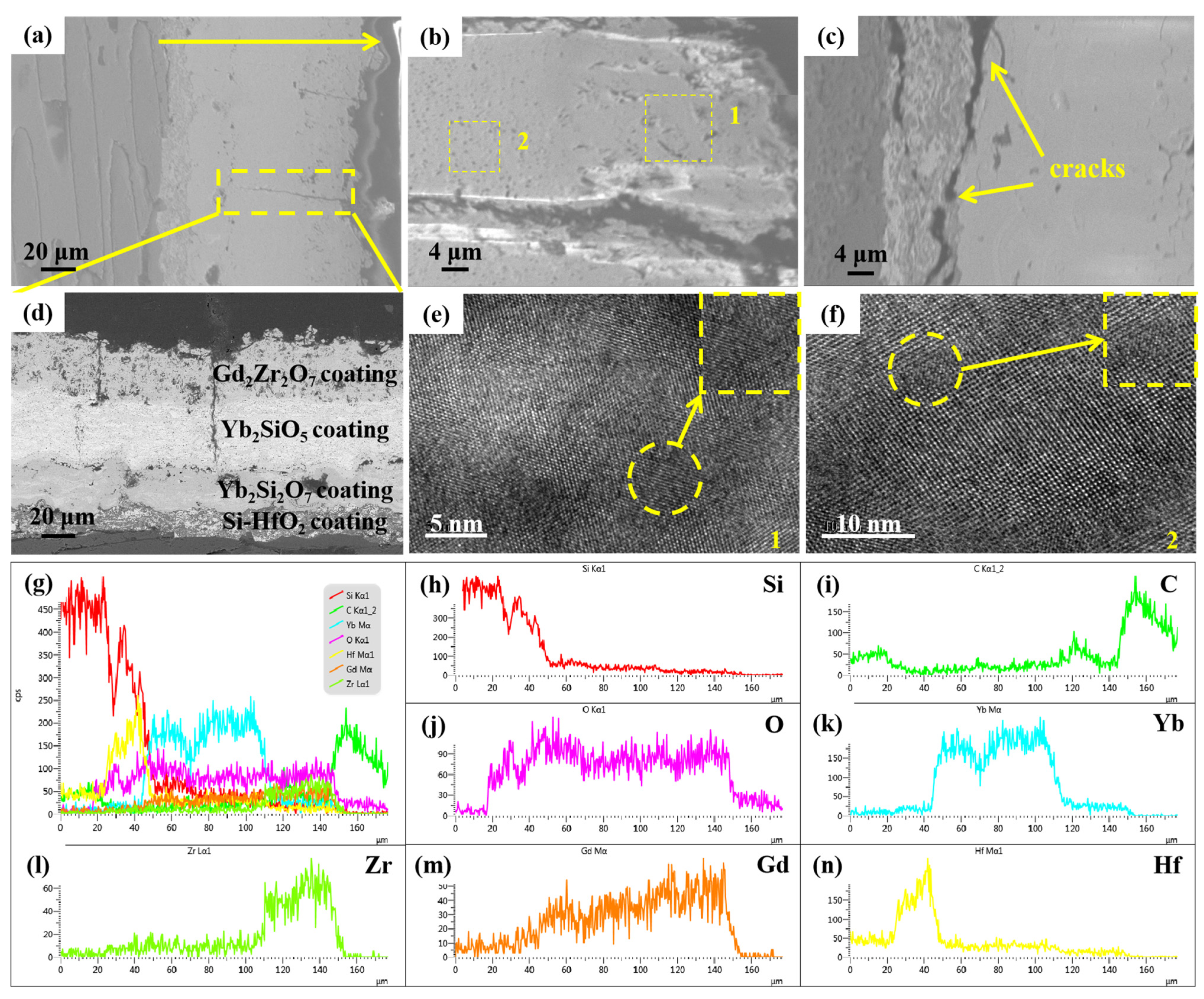
3.2. Microstructure of the Gd2Zr2O7/Yb2SiO5 Interface

The micromorphology and structure of the T/EBC coating interfaces is an important way to understand the coating performance. Figure 5a–d shows the microscopic morphology of the Gd2Zr2O7 cross section and the structure of the Gd2Zr2O7/Yb2SiO5 interface. Figure 5a shows that the coating surface is relatively dense, but there are some local pores. The top of the enlarged view (Figure 5b) resembles a feather-like cylinder. Figure 5c,d shows the Yb2SiO5/Gd2Zr2O7 interface and an enlarged view. The accumulation morphology differs between Yb2SiO5 and Gd2Zr2O7, and the interface can be clearly distinguished.
To better understand the microstructure of the Gd2Zr2O7 coating, the coating was characterized by TEM (Figure 6), with SAED patterns and HRTEM images. Figure 6a shows that the areas marked 1 and 2 in the bright field image are the Gd2Zr2O7 coating. The Gd2Zr2O7 coating is characterized by diffraction rings and diffraction spots, indicating that the coatings have polycrystalline and monocrystalline phase structures. Figure 6b shows the diffraction ring of the Gd2Zr2O7 coating, and the presence of the crystal face index (111) implies the ordered superlattice Gd2Zr2O7 pyrochlore structure [16]. Figure 6c shows the diffraction spots of the Gd2Zr2O7 coating. Crystal plane indices (111), (200), and (220) are mainly observed, which is consistent with the monocrystalline phase characteristics of the Gd2Zr2O7 coating [17]. Figure 6d is the HRTEM image of the Gd2Zr2O7 coating with defect-free structural features (no point or dislocation defects).

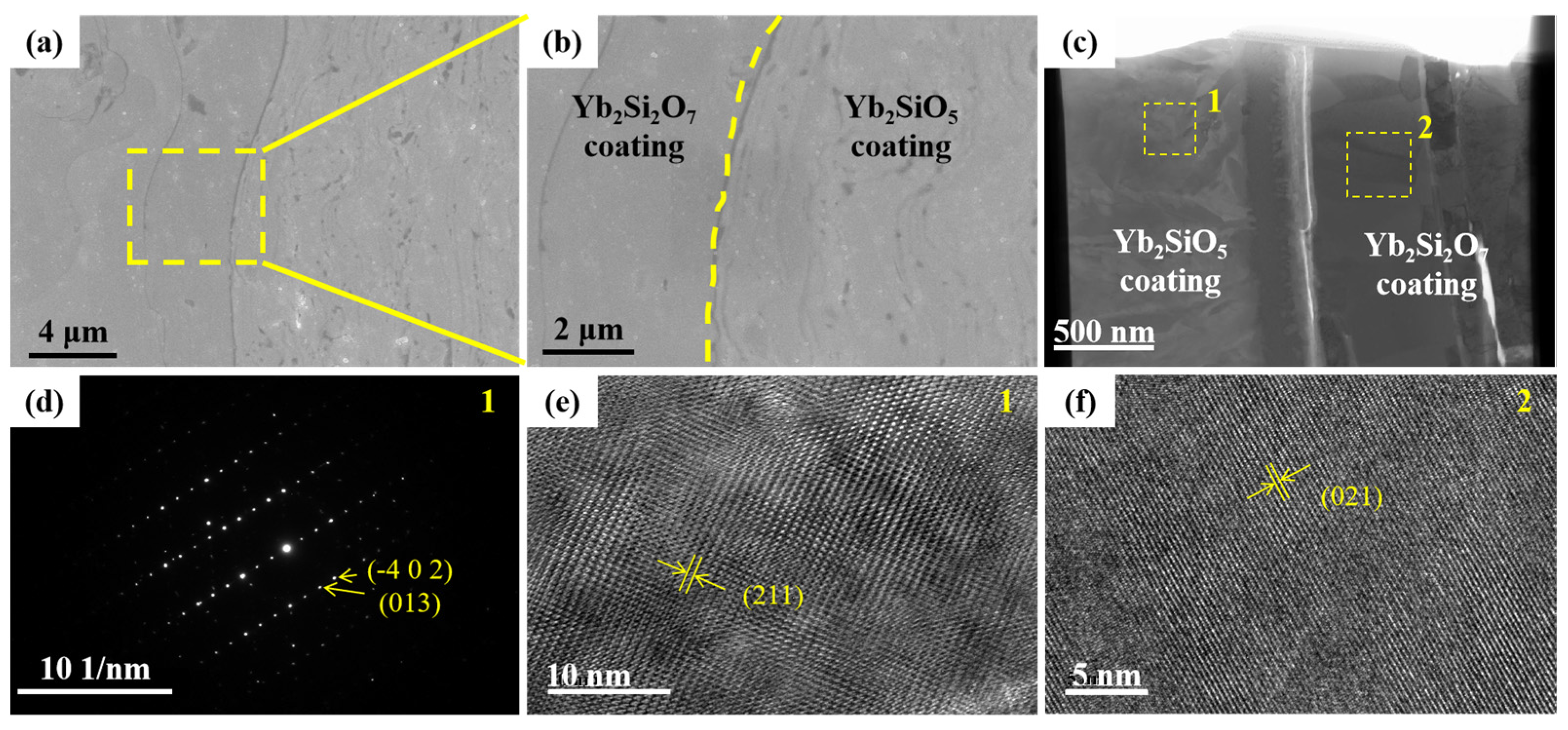
3.3. Microstructure of Yb2SiO5/Yb2SiO7 Interface

The intermediate cross sections of the Yb2SiO5 and Yb2SiO7 coatings and their interfaces were characterized by SEM and TEM. In Figure 7a, the surface has a stacked, layered structure, with obvious stripes between layers that resemble river-like patterns [18,19]. Figure 7b is a microscopic image, and the figure shows nanoscale layers. In Figure 7c, the TEM image of the interface between the Yb2SiO5 and Yb2SiO7 coatings clearly show the two coatings and their interfaces. Figure 7d shows the diffraction spot pattern of the Yb2SiO5 coating for the (−402) and (013) crystal planes [20]. Figure 7e is the HRTEM image of the Yb2SiO5 coating, and it shows the (211) crystal plane and crystal plane spacing of 0.387 nm, which is consistent with the XRD analysis of Figure 3. Figure 7f shows an HRTEM image of the Yb2SiO7 coating, the (021) crystal plane and the crystal plane spacing of 0.319 nm, which is consistent with the XRD analysis of Figure 3. No dislocations or other defects were found in Figure 7e,f, indicating locally ordered structure in the coating.

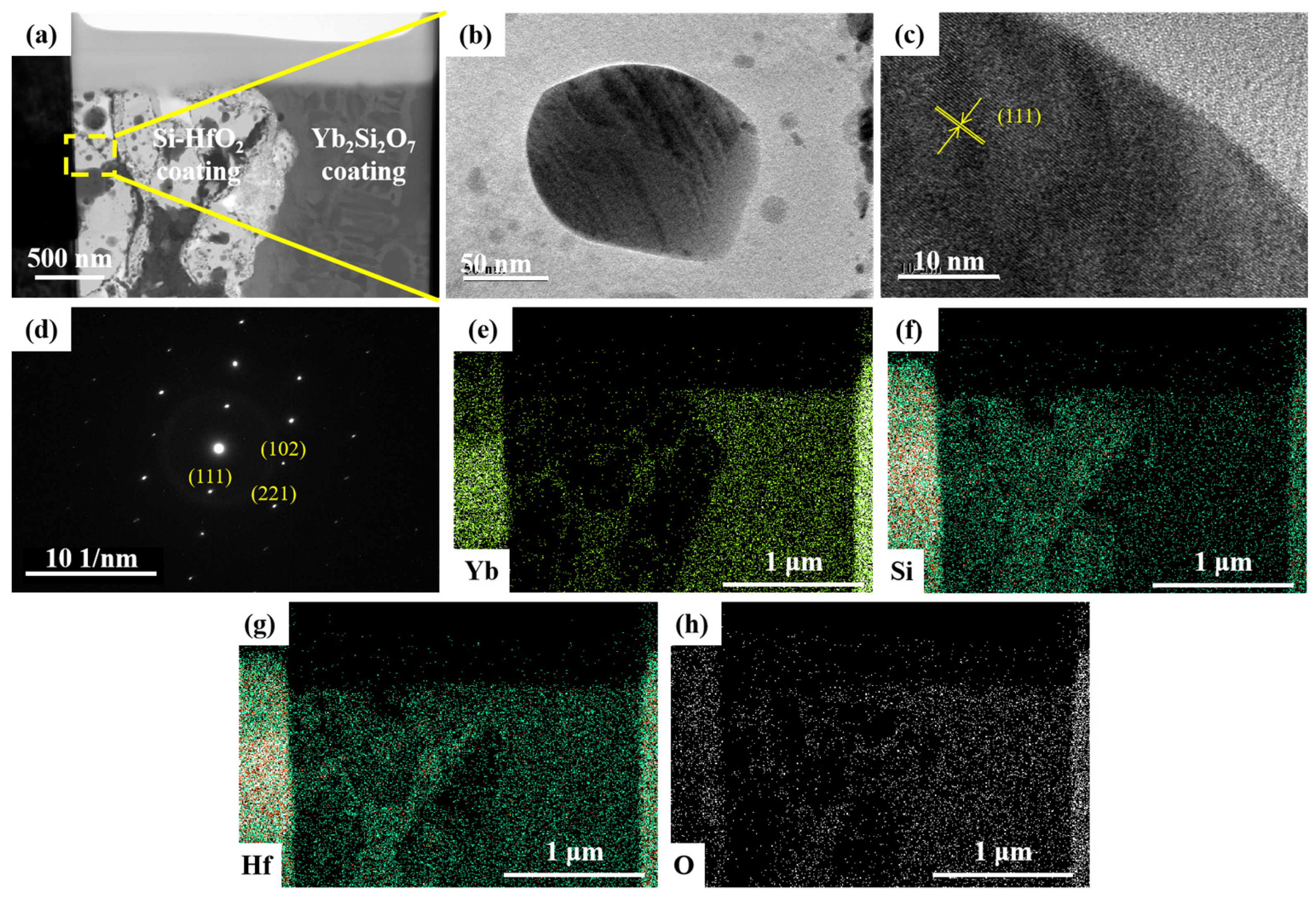
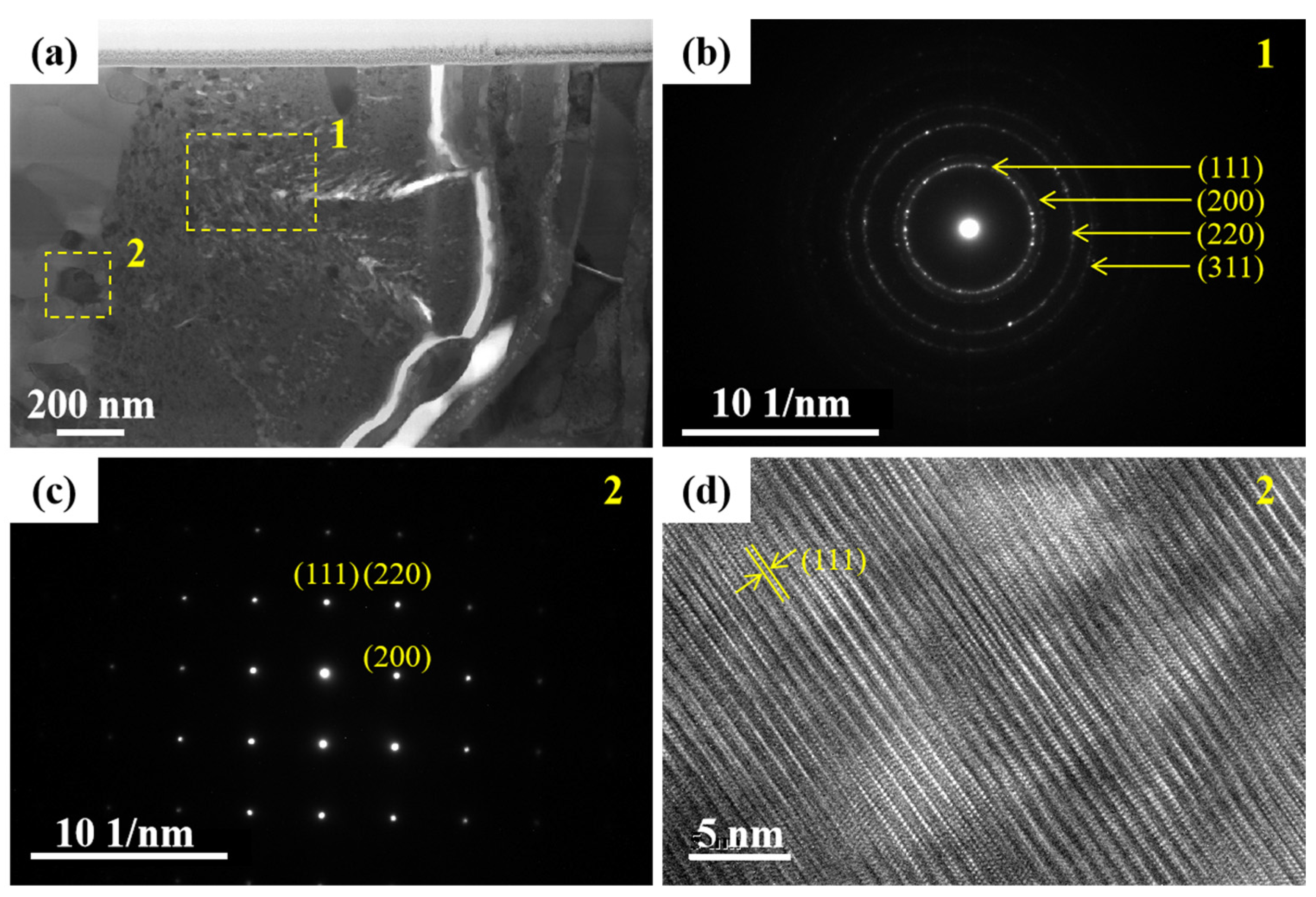
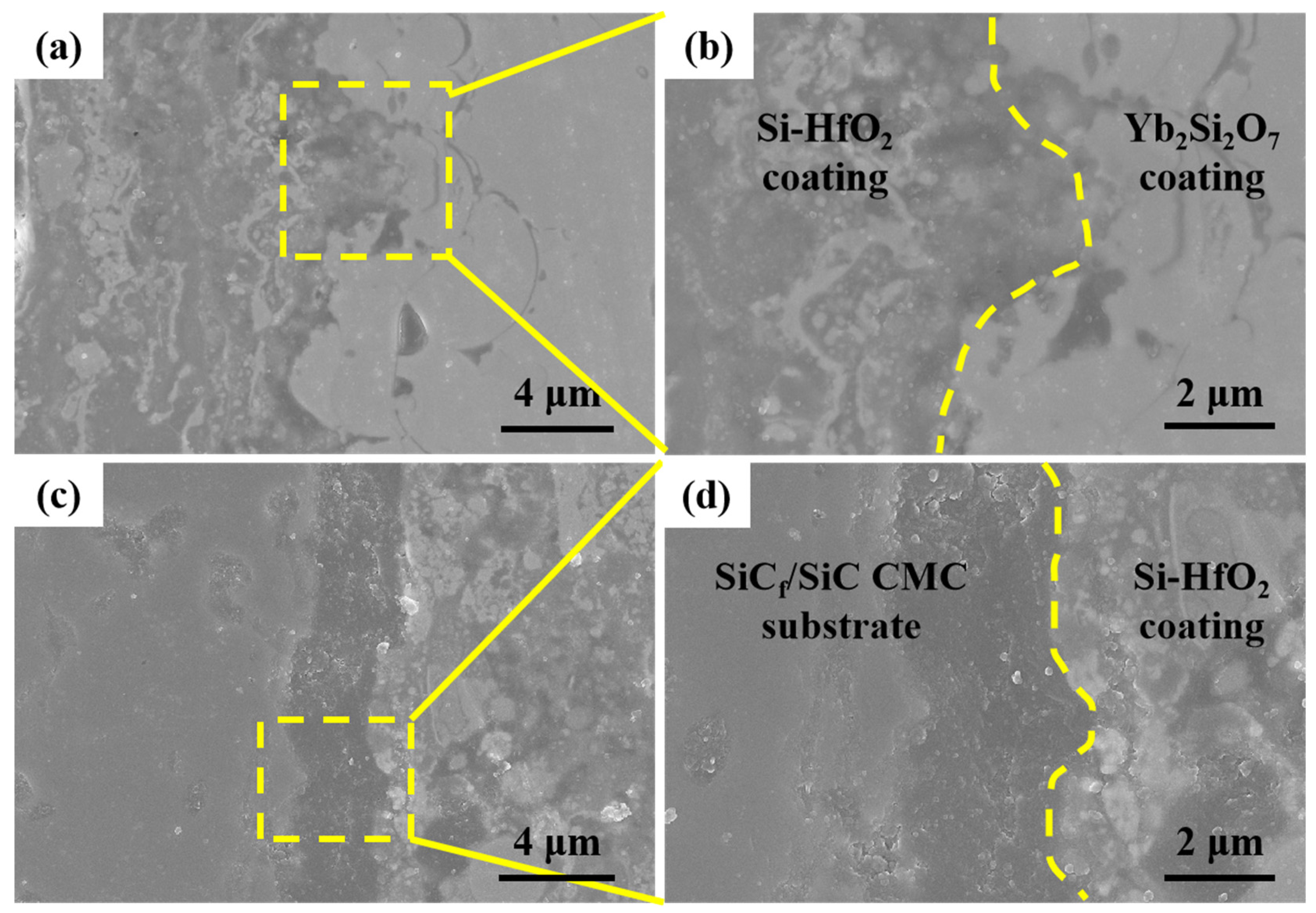
3.4. Microstructure of the Yb2SiO7/Si–HfO2 Interface

The structural characteristics and elemental distributions of the Yb2SiO7 and Si–HfO2 coatings closest to the SiCf/SiC CMC substrate were characterized by TEM and EDS. TEM and diffraction patterns of the Yb2SiO7/Si–HfO2 interface are shown in Figure 8. The interface between the dark-colored Yb2SiO7 coating and the light-colored Si–HfO2 coating is clear, and the binding is tight, without cracks. Figure 8b is an enlarged view of the light-colored Si–HfO2 coating. Nano-HfO2 particles are embedded in the light-colored Si coating. The HRTEM image and diffraction spot analysis of Figure 8c,d confirmed this observation [9,21]. Figure 8e–h shows the EDS patterns of the Yb2SiO7/Si–HfO2 interface. The right side is enriched with Yb and O, indicating that the Yb2SiO7 coating is on the right side. Si is enriched on the left side, indicating that the Si–HfO2 coating is on the left (Figure 8f). A small amount of interdiffusion of Yb and Si is observed at the coating interface [22].
The interfacial boundary of Yb2SiO7/Si–HfO2 is irregular and clear (Figure 9a,b), which is consistent with the observations in Figure 8a. Figure 9c,d shows that the interface of the Si–HfO2 coatings and SiCf/SiC CMC substrate is bonded continuously, and no large holes or cracks are present, which indicates that the PS-PVD technology is able to deposit a dense Si–HfO2 coating on the CMC substrate. The PS-PVD technology is a hybrid coating method technology, which can prepare Si–HfO2 coatings by vapor or liquid deposition [9].

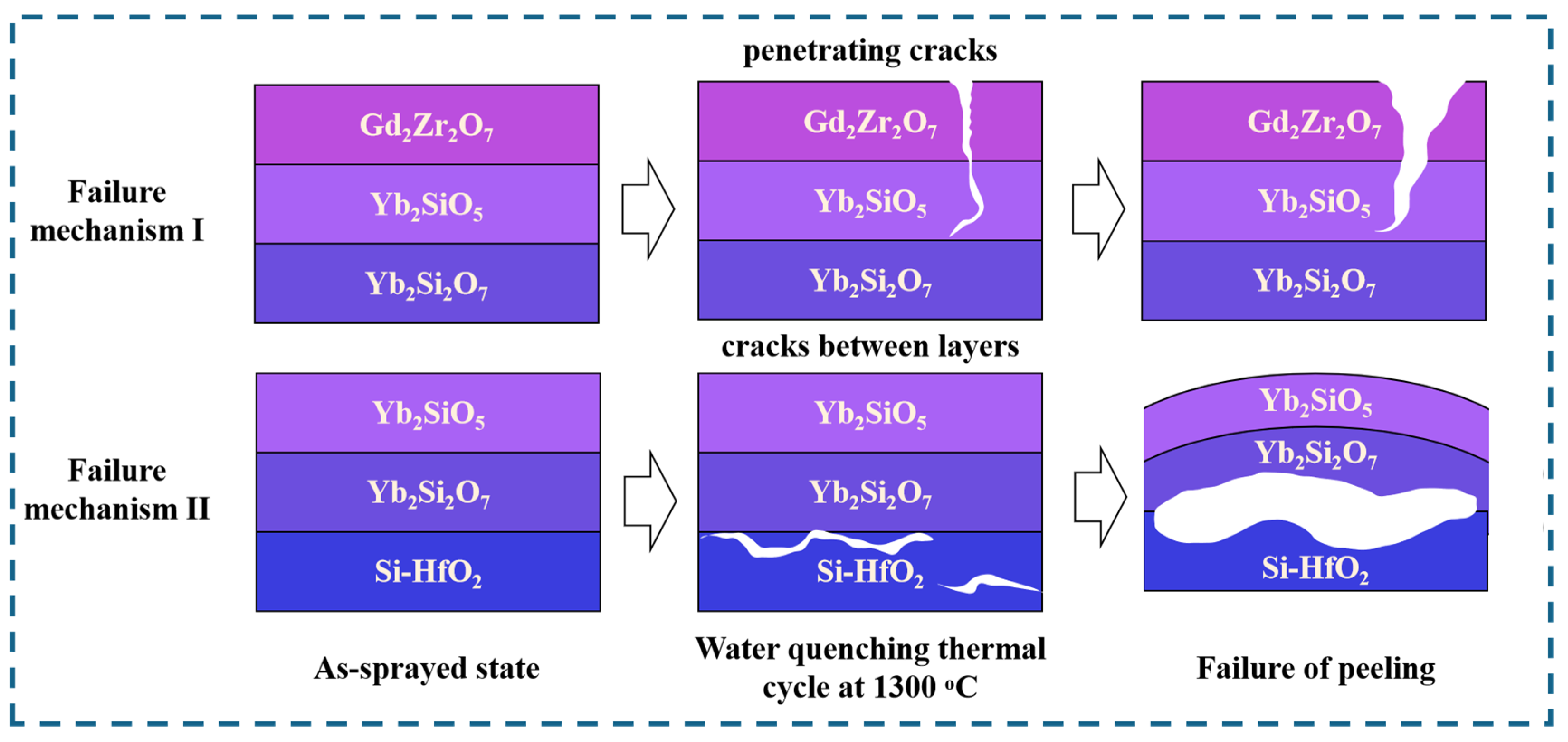
3.5. Water Quenching Test and Failure Mechanism of T/EBCs

The microstructure evolution of T/EBCs was investigated by a water quenching thermal cycle at 1300 °C. The coating surface peeled off after five water quenching thermal cycles. The uppermost surface layer peeled off to half of the original coating, and the lower coating began to warp and break away from the substrate after 10 water quenching thermal cycles. Figure 10 shows the micromorphology and phase analysis of the sample after the water quenching thermal cycle test. The bond between the coating and the substrate is still intact, but penetrating cracks are found in the coating (Figure 10a). Magnifying the image shows that the penetrating cracks come from the surface layer of the coating and penetrate the Yb2SiO7 coating. The porosity of the Yb2SiO5 coating is increased (Figure 10d), and the Gd2Zr2O7 coating is severely damaged (Figure 10b). Figure 10b,c shows two failure modes of the T/EBC coating after water quenching. The first failure mode occurs when cracks generated by the Gd2Zr2O7 coating penetrate the Yb2SiO5 coating and cause failure (Figure 10b). Many point defects and dislocations were observed in the Gd2Zr2O7 and Yb2SiO5 coatings (Figure 10e,f) after water quenching. These defects led to the initiation and propagation of cracks. The second mode of failure is caused by the initiation and propagation of cracks at the Si–HfO2/Yb2Si2O7 interface due to the thermal mismatch, resulting in failure. Due to the difference in the thermal expansion coefficient of Si–HfO2 and Yb2Si2O7, they are 4.5–5.5 × 10⁻⁶ K−1 and 7.0–8.0 × 10⁻⁶ K−1, respectively [23,24,25,26]. The composition distribution of the T/EBC coating cross sections after water quenching is shown in Figure 10g–n. Comparing the element distributions of the as-sprayed and water-quenched coatings shows that the SiCf/SiC matrix and Si–HfO2 matrix contain the same level of Si due to mutual diffusion, while Hf diffuses into the matrix. Gd in the top layer obviously diffuses into the T/EBC coating and Yb2Si2O7 coating. The most obvious element is oxygen, and the oxygen content in the T/EBC coating increases obviously, which indicates that the coating underwent substantial oxidation after water quenching.
A schematic diagram of the failure mechanism with the T/EBC coating after the water quenching thermal cycle is shown in Figure 11. As seen from the figure, the failure mechanism of the coating is divided into two parts: peeling caused by the penetrating cracks on the surface, and whole layer disbonding due to the fusion of cracks between layers. The T/EBC coating was quenched in water after 10 min of the high-temperature thermal cycle at 1300 °C. The sharp temperature difference caused the growth of surface microcracks. As a result, water invaded through microcracks on the surface of Gd2Zr2O7, conforming to the feather-like spraying morphology and reaching the Yb2SiO5 coating. As the amount of water quenching increased, the surface peeling became more pronounced. At the same time, cracks first grew between the Yb2SiO7 and Si–HfO2 layers because the thermal expansion coefficients of the Yb2SiO5 and Yb2SiO7 coatings are similar. Repeated water quenching resulted in the gradual growth and fusion of interlayer cracks, forming large (4 μm) interlayer holes (Figure 10c). Related work has been reported on the water quenching test of TBC coating prepared by PS-PVD technology with the failure mechanism being surface point peeling [27], which is obviously different from this work.

4. Conclusions

Multilayer Si–HfO2/Yb2Si2O7/Yb2SiO5/Gd2Zr2O7 T/EBC composite coatings were prepared on SiC fiber-reinforced SiC ceramic matrix composites (SiCf/SiC CMC) by a PS-PVD method. This study examined the effects of the coating and interface structure on the thermal cycle stability and investigated the failure mechanism. The T/EBC coatings were tested at 1300 °C with 10 cycles of water quenching. The results show the microstructure of the as-sprayed T/EBCs by the PS-PVD method, the cross section is smooth and dense without cracks and pits, for which the interlayer bonding is close, but there is no mutual diffusion of interlayer elements. Before and after water quenching, the structure of the T/EBC composite coatings differs. After water quenching, two failure modes of the T/EBC coatings were observed. One failure mode is that the cracks generated by the Gd2Zr2O7 coating penetrated the Yb2SiO5 coating and caused failure. Another failure mode is caused by the initiation and propagation of cracks at the Si–HfO2/Yb2Si2O7 interface due to thermal mismatch, resulting in failure. In the next step, we will study the thermal cycle failure under different water quenching tests to obtain the performance data of this T/EBCs coating system and provide basic data and technical support for the airworthiness of advanced civil aviation engines.

Author Contributions

Conceptualization, validation, and writing—original draft preparation, J.Z.; investigation, software, validation, and data curation, D.Y.; methodology, project administration, and data curation, S.G.; investigation, writing—review and editing, and supervision, X.Z.; formal analysis, investigation, and visualization, X.L.; software, investigation, X.W. All authors have read and agreed to the published version of the manuscript.

Funding

We would like to acknowledge the financial support from the National Natural Science Foundation of China (51801034), the Guangdong Province Outstanding Youth Foundation (2021B1515020038), and Guangdong Academy of Sciences Program (2020GDASYL–20200104030), and the Guangxi Innovation Driven Development Project (No. AA18242036–2).

Institutional Review Board Statement

Not applicable.

Informed Consent Statement

Not applicable.

Data Availability Statement

Data is contained within the article.

Conflicts of Interest

The authors declare no conflict of interest.

References

  1. Liu, K.; Zhang, K.; Deng, T.; Li, W.; Zhang, H. Comparative study of irradiation effects on nanosized and microsized Gd2Zr2O7 ceramics. Ceram. Int. 2020, 46, 16987–16992. [Google Scholar] [CrossRef]
  2. Lee, K.N.; Eldridge, J.I.; Robinson, R.C. Residual stresses and their effects on the durability of environmental barrier coat-ings for SiC ceramics. J. Am. Ceram. Soc. 2005, 88, 3483–3488. [Google Scholar] [CrossRef]
  3. Chen, P.; Xiao, P.; Li, Z.; Li, Y.; Li, J. Oxidation properties of tri-layer ytterbium-disilicate/mullite/silicon-carbide environment barrier coatings for Cf/SiC composites. Surf. Coat. Technol. 2020, 402, 126329. [Google Scholar] [CrossRef]
  4. Doleker, K.M.; Ozgurluk, Y.; Ahlatci, H.; Karaoglanli, A.C. Evaluation of oxidation and thermal cyclic behavior of YSZ, Gd2Zr2O7 and YSZ/Gd2Zr2O7 TBCs. Surf. Coat. Technol. 2019, 371, 262–275. [Google Scholar] [CrossRef]
  5. Díaz-Guillén, J.; Fuentes, A.; Díaz-Guillén, M.; Almanza, J.; Santamaria, J.; Leon, C. The effect of homovalent A-site substitutions on the ionic conductivity of pyrochlore-type Gd2Zr2O7. J. Power Sources 2009, 186, 349–352. [Google Scholar] [CrossRef]
  6. Kong, L.; Karatchevtseva, I.; Gregg, D.J.; Blackford, M.G.; Holmes, R.; Triani, G. Gd2Zr2O7 and Nd2Zr2O7 pyrochlore prepared by aqueous chemical synthesis. J. Eur. Ceram. Soc. 2013, 33, 3273–3285. [Google Scholar] [CrossRef]
  7. Garcia, E.; Sotelo-Mazon, O.; Poblano-Salas, C.; Trapaga, G.; Sampath, S. Characterization of Yb2Si2O7–Yb2SiO5 composite environmental barrier coatings resultant from in situ plasma spray processing. Ceram. Int. 2020, 46, 21328–21335. [Google Scholar] [CrossRef]
  8. Zhong, X.; Niu, Y.; Li, H.; Zhu, T.; Song, X.; Zeng, Y.; Zheng, X.; Ding, C.; Sun, J. Comparative study on high-temperature per-formance and thermal shock behavior of plasma-sprayed Yb2SiO5 and Yb2Si2O7 coatings. Surf. Coat. Tech. 2018, 349, 636–646. [Google Scholar] [CrossRef]
  9. Harder, B.J. Oxidation performance of Si–HfO2 environmental barrier coating bond coats deposited via plasma spray-physical vapor deposition. Surf. Coat. Tech. 2020, 384, 125311. [Google Scholar] [CrossRef]
  10. Ouyang, Z.; Yang, Y.; Sun, J. Electroluminescent Yb2O3:Er and Yb2Si2O7:Er nanolaminate films fabricated by atomic layer deposition on silicon. Opt. Mater. 2018, 80, 209–215. [Google Scholar] [CrossRef]
  11. Chen, P.; Pan, L.; Xiao, P.; Li, Z.; Pu, D.; Li, J.; Pang, L.; Li, Y. Microstructure and anti-oxidation properties of Yb2Si2O7/SiC bi-layer coating for C/SiC composites. Ceram. Int. 2019, 45, 24221–24229. [Google Scholar] [CrossRef]
  12. Bakan, E.; Mack, D.E.; Mauer, G.; Mücke, R.; Vaßen, R.; Troczynski, T. Porosity–property relationships of plasma-sprayed Gd2Zr2O7/YSZ thermal barrier coatings. J. Am. Ceram. Soc. 2015, 98, 2647–2654. [Google Scholar] [CrossRef]
  13. Yang, H.; Yang, Y.; Cao, X.; Huang, X.; Li, Y. Thermal shock resistance and bonding strength of tri-layer Yb2SiO5/mullite/Si coating on SiCf/SiC composites. Ceram. Int. 2020, 46, 27292–27298. [Google Scholar] [CrossRef]
  14. Ridley, M.; Opila, E. Thermochemical stability and microstructural evolution of Yb2Si2O7 in high-velocity high-temperature water vapor. J. Eur. Ceram. Soc. 2021, 41, 3141–3149. [Google Scholar] [CrossRef]
  15. Robertson, A.L.; Solá, F.; Zhu, D.; Salem, J.; White, K.W. Microscale fracture mechanisms of HfO2–Si environmental barrier coatings. J. Eur. Ceram. Soc. 2019, 39, 2409–2418. [Google Scholar] [CrossRef]
  16. Zhang, F.; Lang, M.; Ewing, R.C. Atomic disorder in Gd2Zr2O7 pyrochlore. Appl. Phys. Lett. 2015, 106, 191902. [Google Scholar] [CrossRef]
  17. Huang, Z.; Qi, J.; Zhou, M.; Gong, Y.; Shi, Q.; Yang, M.; Han, W.; Cao, Z.; Peng, S.; Lu, T. A facile solvothermal method for high-quality Gd2Zr2O7 nanopowder preparation. Ceram. Int. 2018, 44, 1334–1342. [Google Scholar] [CrossRef]
  18. Zou, B.; Khan, Z.S.; Gu, L.; Fan, X.; Huang, W.; Wang, Y.; Zhao, Y.; Wang, C.; Yang, K.; Ma, H.; et al. Microstructure, oxidation protection and failure mechanism of Yb2SiO5/LaMgAl11O19 coating deposited on C/SiC composites by atmospheric plasma spraying. Corros. Sci. 2012, 62, 192–200. [Google Scholar] [CrossRef]
  19. Han, B.; Zhang, R.; Fang, D. Preparation and characterization of highly porous Yb2SiO5 ceramics using water-based freeze-casting. J. Porous Mater. 2016, 23, 563–568. [Google Scholar] [CrossRef]
  20. Khan, Z.; Zou, B.; Huang, W.; Fan, X.; Gu, L.; Chen, X.; Zeng, S.; Wang, C.; Cao, X. Synthesis and characterization of Yb and Er based monosilicate powders and durability of plasma sprayed Yb2SiO5 coatings on C/C–SiC composites. Mater. Sci. Eng. B 2012, 177, 184–189. [Google Scholar] [CrossRef]
  21. Cosnier, V.; Olivier, M.; Théret, G.; André, B. HfO2–SiO2 interface in PVD coatings. J. Vac. Sci. Technol. A 2001, 19, 2267–2271. [Google Scholar] [CrossRef]
  22. Holgate, C.S.; Yang, Y.; Levi, C.G. Reactive crystallization in HfO2 exposed to molten silicates. J. Eur. Ceram. Soc. 2021, 41, 5686–5695. [Google Scholar] [CrossRef]
  23. Zhang, X.F.; Song, J.B.; Deng, Z.Q.; Wang, C.; Niu, S.P.; Liu, G.; Deng, C.M.; Deng, C.G.; Liu, M.; Zhou, K.S.; et al. Interface evolu-tion of Si/Mullite/Yb2SiO5 PS-PVD environmental barrier coatings under high temperature. J. Eur. Ceram. Soc. 2020, 40, 1478–1487. [Google Scholar] [CrossRef]
  24. Zhang, X.; Wang, C.; Ye, R.; Deng, C.; Liang, X.; Deng, Z.; Niu, S.; Song, J.; Liu, G.; Liu, M.; et al. Mechanism of vertical crack formation in Yb2SiO5 coatings deposited via plasma spray-physical vapor deposition. J. Mater. 2020, 6, 102–108. [Google Scholar] [CrossRef]
  25. Wang, C.; Liu, M.; Feng, J.; Zhang, X.; Deng, C.; Zhou, K.; Zeng, D.; Guo, S.; Zhao, R. Water vapor corrosion behavior of Yb2SiO5 environmental barrier coatings prepared by plasma spray-physical vapor deposition. Coatings 2020, 10, 392. [Google Scholar] [CrossRef]
  26. Dong, L.; Liu, M.; Zhang, X.; Yang, G.; Wang, C.; Fan, J.; Zhou, K. Infiltration thermodynamics in wrinkle-pores of thermal sprayed coatings. Appl. Surf. Sci. 2021, 543, 148847. [Google Scholar] [CrossRef]
  27. Zhang, X.F.; Zhou, K.S.; Liu, M.; Deng, C.M.; Deng, C.G.; Chen, H.T. Thermal shock analysis of surface Al-modified 7YSZ nano-thermal barrier coating. J. Inorg. Mater. 2017, 32, 973–979. [Google Scholar]
Figure 1. (a) Schematic diagram of T/EBCs coating structure. The SEM images of each coating powder of T/EBCs: (b) Si–HfO2; (c) Yb2Si2O7; (d) Yb2SiO5; (e) Gd2Zr2O7.
Coatings 11 00889 g001
Figure 2. SEM images and EDS analysis of T/EBCs: (a) micromorphology of surface layer; (b) enlargement of (a); (c) point scan analysis; (d) micromorphology of cross-section; (e) enlargement of (d); (f) line scan analysis. Composition distribution of T/EBCS coatings cross section: (g) all elements; (h) Si; (i) C; (j) O; (k) Yb; (l) Zr; (m) Gd; (n) Hf.
Coatings 11 00889 g002
Figure 3. XRD patterns of each coating in T/EBCs coating.
Coatings 11 00889 g003
Figure 4. FIB-SEM of cross-section with T/EBCs coating: (a) cross-sectional peeling diagram; (b) positions 1; (c) positions 2; (d) positions 3.
Coatings 11 00889 g004
Figure 5. Cross-sectional micromorphology: (a) Gd2Zr2O7 coatings; (b) enlargement of (a); (c) Gd2Zr2O7/Yb2SiO5 interface; (d) enlargement of (c).
Coatings 11 00889 g005
Figure 6. TEM image: (a) bright field image of Gd2Zr2O7 coating; (b) the SAED patterns of Gd2Zr2O7 coating the areas marked 1 in (a); (c) the SAED patterns of Gd2Zr2O7 coating the areas marked 2 in (a); (d) HRTEM image of Gd2Zr2O7 coating the areas marked 2 in (a).
Coatings 11 00889 g006
Figure 7. Cross-section micromorphology: (a) Yb2SiO5/Yb2SiO7 interface; (b) enlargement of (a); TEM images: (c) bright field image of Yb2SiO5/Yb2SiO7 interface; (d) the SAED pattern of the areas marked 1 in (c); (e) HRTEM image of the areas marked 1 in (c); (f) HRTEM image of the areas marked 2 in (c).
Coatings 11 00889 g007
Figure 8. TEM image: (a) bright field image of Yb2SiO7/Si–HfO2 Interface; (b) the TEM patterns of the HfO2; (c) HRTEM image of the HfO2; (d) the SAED patterns of the HfO2. EDS patterns of the Yb2SiO7/Si-HfO2 interface: (e) Yb; (f) Si; (g) Hf; (h) O.
Coatings 11 00889 g008
Figure 9. Cross-section micromorphology: (a) Si–HfO2/Yb2SiO7 interface; (b) enlargement of (a); (c) SiC/C/Si–HfO2 interface; (d) enlargement of (c).
Coatings 11 00889 g009
Figure 10. Micromorphology and phase analysis after water quenching: (a) cross-section; (b) TEM image of cracks in Gd2Zr2O7 coatings; (c) TEM image of cracks in SiC/C/Si–HfO2 interface; (d) crack enlargement of (a); (e) dislocation defect in the Gd2Zr2O7 coating at area marked1 in (b); (f) dislocation defect in the Yb2SiO5 coating at area marked 2 in (b). Composition distribution of T/EBCS coatings cross section after water quenching: (g) all elements; (h) Si; (i) C; (j) O; (k) Yb; (l) Zr; (m) Gd; (n) Hf.
Coatings 11 00889 g010
Figure 11. Schematic diagram of failure mechanism with T/EBCs coating after water quenching.
Coatings 11 00889 g011
Table 1. Process parameters of PS-PVD for each coating.
CoatingsPre-Heat Temperature (°C)Spraying Distance (mm)Current
(A)
Ar
(NLPM)
H2 (NLPM)He (NLPM)
Si-10%HfO2500400165011060
Yb2Si2O750010002600100020
Yb2SiO550010002600100020
Gd2Zr2O710001000260035060
Publisher’s Note: MDPI stays neutral with regard to jurisdictional claims in published maps and institutional affiliations.

