Article

Evolution of High-Quality Homoepitaxial CVD Diamond Films Induced by Methane Concentration

1
College of Materials Science and Engineering, Inner Mongolia University of Technology, Hohhot 010051, China
2
Institute of Wide Band Gap Semiconductors, Xi’an Jiaotong University, Xi’an 710049, China
3
Inner Mongolia Key Laboratory of Thin Film and Coatings, Hohhot 010051, China
*
Author to whom correspondence should be addressed.
Coatings 2021, 11(8), 888; https://doi.org/10.3390/coatings11080888
Submission received: 29 June 2021 / Revised: 13 July 2021 / Accepted: 23 July 2021 / Published: 26 July 2021
(This article belongs to the Collection Coatings: 10th Anniversary)

Abstract

:
In this paper, we successfully synthesized homoepitaxial diamond with high quality and atomically flat surface by microwave plasma chemical vapor deposition. The sample presents a growth rate of 3 μm/h, the lowest RMS of 0.573 nm, and the narrowest XRD FWHM of 31.32 arcsec. An effect analysis was also applied to discuss the influence of methane concentration on the diamond substrates.

1. Introduction

Diamond offers significant advantages such as large bandgap energy, high electrical breakdown strength, high carrier mobilities, high thermal conductivity, high Johnson Keyes, and Baliga quality factors, making it suitable for high frequency, high power, and high temper electron device applications [1,2,3,4,5]. The lack of high-quality substrates, however, hindered the development of single-crystal diamonds (SCDs) as an electronic material.
In the past decade, diamond films were studied by numerous methods, such as HF-CVD, DC arc jet CVD, DC-PCVD, and HTHP methods [6,7]. The microwave plasma chemical vapor deposition (MPCVD) technique is the only method that synthesizes high-quality SCDs (device grade [8]) with an atomically flat surface. However, some critical issues need to be solved before CVD diamond films utilizing in electronic devices. For high-value-added applications such as radiation-hard detectors [9,10], Raman lasers [11], and electronic devices [12], one of the key requirements is to decrease the charge trapping factors such as structural defects, point defects, and nitrogen impurities [13]. Thus, research on synthesis device-grade high-quality SCDs in a pure methane–hydrogen mixed gas without N addition is of vital importance and urgent necessity to advance diamond-based applications development.
Although the effect of the methane concentration on the process of CVD synthesis was reported [14,15,16,17,18], device-grade SCDs (FWHM < 60 arcsec, RMS < 1 nm) produced in a pure methane–hydrogen microwave plasma were not addressed in the previous methane optimization studies.
In this work, a microwave plasma CVD growth of SCDs films without the addition of other gases was investigated. Methane concentration was varied to evaluate the influence on the final morphology and on the growth rate, surface roughness values, and crystalline quality.

2. Materials and Methods

The fabricated processes were carried out in AsteX 5200 reactor (Seki Technotron Corp., Tokyo, Japan) at 2.45 GHz. Homoepitaxial diamond films were deposited on commercial 3 × 3 × 1 mm3 high-temperature and high-pressure (HPHT) synthesized type Ib (100)-oriented substrates, purchased from the Xi’an DMT Semiconductor Technology Co., Ltd (Xi’an, China). We chose this orientation since a higher-quality diamond was easier to obtain on this growth sector [19,20]. All substrates were polished to obtain surface roughness below 1 nm without misorientation angle and were cleaned in a mixture acid (H2SO4:HNO3:HClO4 = 31.2:36:11.4) at 250 °C for one hour, then treated with mixed alkali (NH4OH:H2O2:H2O = 4:3:9) at 80 °C for 10 min to remove the non-diamond phase. Afterward, the substrates were treated by the hydrogen plasma in 400 sccm gas flow in total with 2% oxygen for 60 min to remove the mechanical damage caused by polishing.
During the SCD epitaxy, a polycrystal diamond (PCD) rim often appears around SCDs, leading to the shrinkage of the SCDs; hence, the Mo pocket substrate holder was applied to decrease the PCD rims and optimize the growth process [21,22]. The hydrogen and the methane in the purity of 6N and 5N5 were introduced into the chamber through a mass flow controller.
The base pressure was realized by a rotary pump to 0.1 Torr after the substrate was placed on the Mo holder. In the process of the growth, the chamber pressure, temperature, microwave power, and deposition time were 78 Torr, 1015 ± 20 °C, 3.9 kW, and 3 h, respectively. The temperature of the sample surface was adjusted by microwave power [23] and measured by an infrared radiation thermometer through the quartz windows on the top of the chamber. There was no extra heating apparatus under the substrate holder. The total reaction gas was 500 sccm, and CH4/H2 flow rates were varied at 6%, 6.2%, 6.4%, 7%, and 8% to study its influence on the growth of SCDs.
The growth rate was estimated by the growth time and thickness increment of the substrates determined by an auto micrometer caliper with the accuracy of 0.01 mm.
The morphologies of the diamond films were studied by the optical microscope, scanning electron microscopy (HITACHI SU-8010), and atomic force microscopy (AFM, INNOVA Bruker Corp., Billerica, MA, USA). The quality of the films was characterized by X-ray diffraction (XRD, PANalytical The Analytical X-ray Company, Malvern, UK) and Raman spectra (Renishaw InVia Qontor, 532 nm, Wotton Underage, UK).

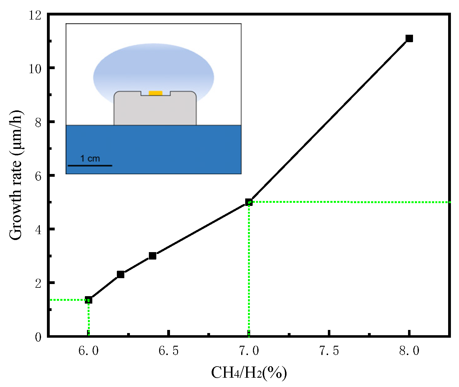
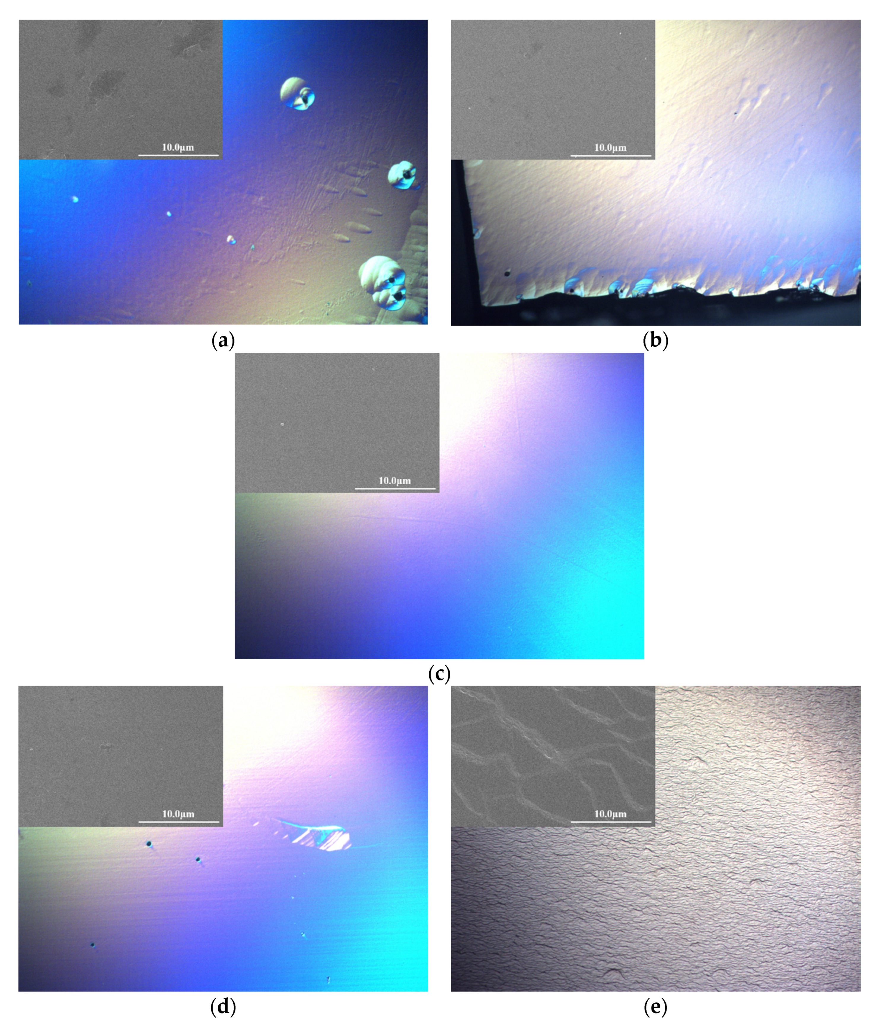
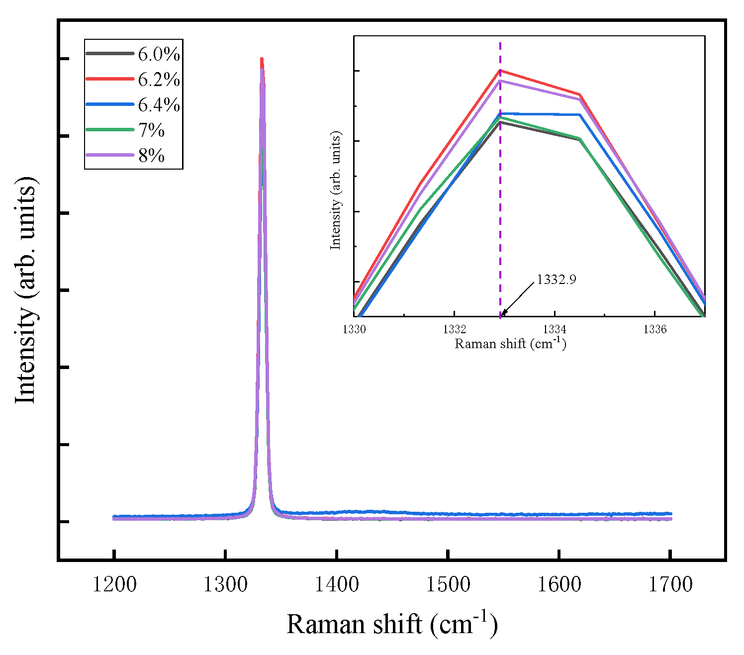
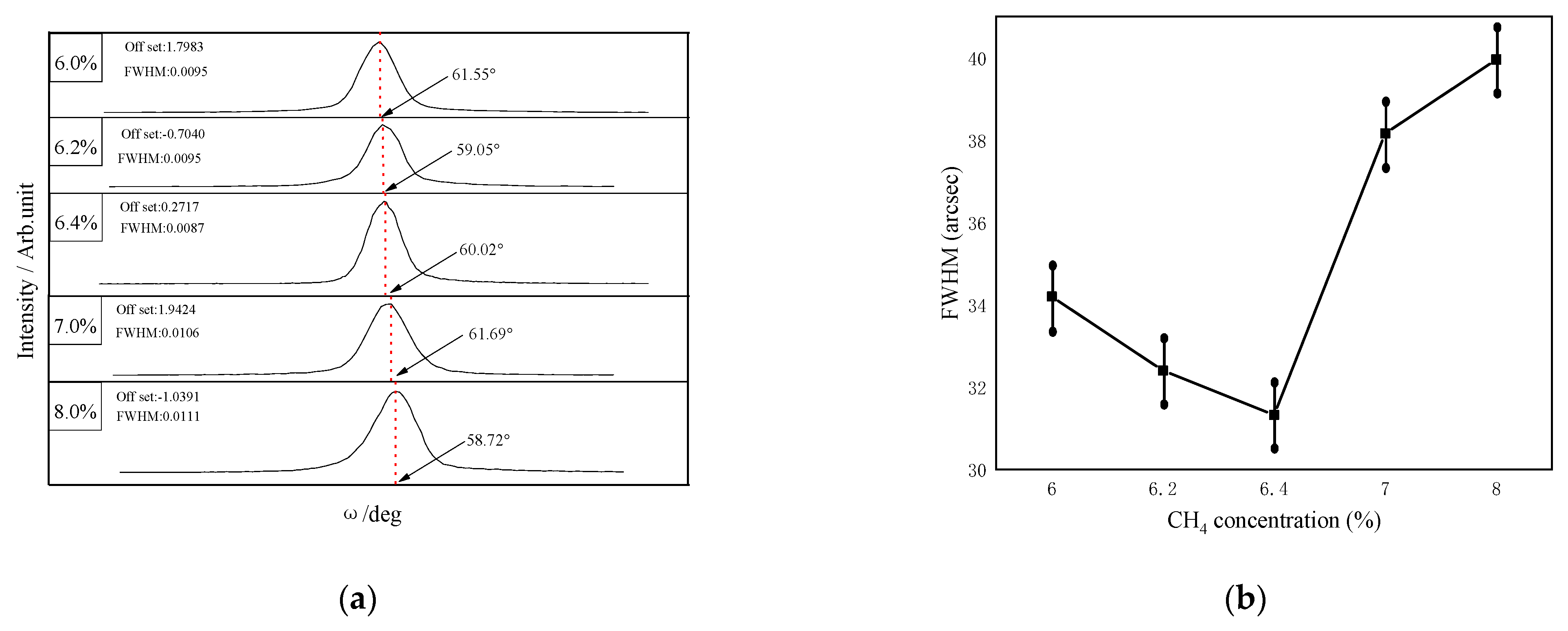
3. Results and Discussion

Figure 1 shows the graph relating methane concentration to the growth rate. The inset illustrates the position of the diamond sample in the Mo pocket. The growth rate increased almost linearly with methane concentration. For instance, the value of growth rate is 1.35 μm/h for the methane concentration of 6%, while the value increases to 5 μm/h at a methane concentration of 7%. This can be explained by that the concentration of carbon radicals increased with the increase of methane concentration, and a large proportion of methane molecules dissociated to generate radicals, which were considered to be involved in the nucleation process of the diamond.
Figure 2 shows an optical image (50×) of the diamond obtained during the experiments (the inset shows the SEM image (5000×) of the diamond). With 6% of the methane, there are many large rounded hillocks with several pits on the surface of diamond film. This phenomenon could be a consequence of high atomic hydrogen concentration that causes a high etch rate during growth at high microwave power [24]. With the increase of the methane concentration, the large rounded hillocks disappear, and the surface morphology is improved, the substrate surface is very smooth at 6.4% methane. However, unexpected crystallites and step-bunching are observed on the films grown with 7% and 8% of methane. From the substrate surface morphology, the optimum methane content can be found at 6.4%.
Figure 3 shows the AFM images of the substrates with an area of 5 × 5 μm2. The root means square (RMS) roughness from the AFM pictures are 1.36, 1.1, 0.573, 1.41, and 35.7 nm for the samples grown with 6%, 6.2%, 6.4%, 7%, and 8% of methane, respectively. These films are atomically flat over the area. The variety trend of the roughness as a function of methane concentration is plotted in Figure 3. The roughness decreases from 1.36 to 0.573 nm, which means that appropriate methane content in the reaction gas can reduce the surface roughness. However, with further increasing the flow rate of methane, the secondary nucleation effect of methane is enhanced, which would make the surface rough.
In order to compare the quality of the samples grown at different methane concentrations, Raman spectroscopy was applied, which is shown in Figure 4. The strong Raman scattering peak of the diamond phase is observed at about 1332.9 cm−1, with a full width at half maximum (FWHM) of 6.6–6.8 cm−1, which is the characteristic peak of the sp3 structural of diamond [25]. There is no peak of the non-diamond phase and no obvious stress concentration area, and there are no components of disordered carbon in the Raman spectra, indicating the high quality of SCD [26,27].
Figure 5a shows the XRD rocking curve patterns taken from the growth surface of the diamonds. The fitted FWHM of the XRD peak is plotted as a function of CH4 concentration (Figure 5b) as well. Variation of the rocking curve peak position is due to the original HPHT substrate and mechanical bending of the crystal [28,29]. The X-ray intensity of a single pixel is extracted from the image series scanned by a given rocking curve, and the peak position and width of the pixel are extracted by Gaussian fitting. The relatively low FWHM of all samples are narrower than 40 arcsec, comparable with the electronic grade SCDs commercially purchased from EDP Ltd., illustrates a high-quality diamond layer. With the increase of methane concentration, the corresponding FWHM is decreased, which can be attributed to the increased SP3 bonding in the substrate. With further increasing the methane content, FWHM presented an increasing trend, caused by SP3 bonding transforms into SP2 bonding, and the substrate surface is graphitized. Raman analysis provides qualitatively compatible results. These analyses revealed that the 6.4% methane concentration is the most appropriate ratio with FWHM in 31.32 arcsec, which is consistent with the dependence observed of the morphology analysis. It is evident that a proper concentration of methane is favorable to achieve high-quality SCDs with atomically smooth surface.

4. Conclusions

The purpose of this paper was to find the effect of the methane concentration for high-quality SCDs synthesis. Substrates with an atomically smooth surface and high crystallinity were successfully fabricated. Under the optimized condition in 6.4% methane concentration, the sample presents a proper growth rate (3 μm/h), lowest RMS (0.573 nm), and narrowest XRD FWHM (31.32 arcsec). These facts are expected to help realize the high-quality and long-term stable deposition required for device-grade SCDs production.

Author Contributions

Conceptualization, P.Z. and Y.W.; methodology, S.H.; software, S.Y.; validation, and L.Z., H.W.; formal analysis, H.W.; investigation, S.H.; resources, H.W.; data curation, C.G.; writing—original draft preparation, P.Z.; writing—review and editing, H.W.; visualization, P.Z.; supervision, W.C.; project administration, S.Y.; funding acquisition, W.M. All authors have read and agreed to the published version of the manuscript.

Funding

This research was funded by the National Natural Science Foundation of China (No. 51964035) and the Postgraduate Research Innovation Project of Inner Mongolia Autonomous Region (BZ2020032).

Institutional Review Board Statement

Not applicable.

Informed Consent Statement

Not applicable.

Data Availability Statement

Data sharing not applicable.

Conflicts of Interest

The authors declare no conflict of interest.

References

  1. Gajewski, W.; Achatz, P.; Williams, O.A.; Haenen, K.; Bustarret, E.; Stutzmann, M.; Garrido, J. Electronic and optical properties of boron-doped nanocrystalline diamond films. Phys. Rev. B 2009, 79, 045206. [Google Scholar] [CrossRef] [Green Version]
  2. Angus, J.C.; Hayman, C.C. Low-Pressure, metastable growth of diamond and diamondlike phases. Science 1988, 241, 913–921. [Google Scholar] [CrossRef] [PubMed]
  3. Kawarada, H.; Yamada, T.; Xu, D. Diamond MOSFETs using 2D hole gas with 1700V breakdown voltage. In Proceedings of the 2016 28th International Symposium on Power Semiconductor Devices and ICs (ISPSD), Prague, Czech Republic, 12–16 June 2016. [Google Scholar]
  4. Koizumi, S.; Watanabe, K.; Hasegawa, M.; Kanda, H. Ultraviolet emission from a diamond pn junction. Science 2001, 292, 1899–1901. [Google Scholar] [CrossRef] [PubMed] [Green Version]
  5. Liu, J.W.; Liao, M.Y.; Imura, M.; Matsumoto, T.; Shibata, N.; Ikuhara, Y.; Koide, Y. Control of normally on/off characteristics in hydrogenated diamond metal-insulator-semiconductor field-effect transistors. J. Appl. Phys. 2015, 118, 115704. [Google Scholar] [CrossRef]
  6. Liu, X.; Lu, P.; Wang, H.; Ren, Y.; Tan, X.; Sun, S.; Jia, H. Morphology and structure of Ti-doped diamond films prepared by microwave plasma chemical vapor deposition. Appl. Surf. Sci. 2018, 442, 529–536. [Google Scholar] [CrossRef]
  7. Zhang, T.; Zou, Y. The effect of deposition parameters on the growth rate of microcrystalline diamond powders synthesized by HFCVD method. Coatings 2017, 7, 95. [Google Scholar] [CrossRef] [Green Version]
  8. Takeuchi, D.; Watanabe, H.; Yamanaka, S.; Okushi, H.; Kajimura, K. Defects in device grade homoepitaxial diamond thin films grown with ultra-low CH4/H2 conditions by microwave-plasma chemical vapor deposition. Phys. Status Solidi (a) 1999, 174, 101–115. [Google Scholar] [CrossRef]
  9. Kumar, A.; Topkar, A.; Das, D. Prototyping and performance study of a single crystal diamond detector for operation at high temperatures. Nucl. Instrum. Meth. A 2017, 858, 12–17. [Google Scholar] [CrossRef]
  10. Su, K.; He, Q.; Zhang, J.; Ren, Z.; Liu, L.; Zhang, J.; Ouyang, X.; Hao, Y. Device performance of chemical vapor deposition monocrystal diamond radiation detectors correlated with the bulk diamond properties. J. Phys. D Appl. Phys. 2021, 54, 145105. [Google Scholar] [CrossRef]
  11. Mildren, R.P.; Sabella, A.; Kitzler, O.; Spence, D.J.; McKay, A.M. Diamond raman laser design and performance. Opt. Eng. Diam. 2013, 239–276. [Google Scholar] [CrossRef]
  12. Wang, Y.-F.; Wang, W.; Wei, J.; Jiao, B.; Xu, D.; Chang, X.; Abbasi, H.N.; Song, W.; Chen, G.; Wang, H.-X. Electrochemical route to bio-compatible fluorine-terminated diamond surface. Carbon 2021, 176, 83–87. [Google Scholar] [CrossRef]
  13. Shimaoka, T.; Kaneko, J.H.; Tsubota, M.; Shimmyo, H.; Watanabe, H.; Chayahara, A.; Umezawa, H.; Shikata, S.-I. High-performance diamond radiation detectors produced by lift-off method. EPL Europhys. Lett. 2016, 113, 62001. [Google Scholar] [CrossRef]
  14. Sedov, V.; Martyanov, A.; Khomich, A.; Savin, S.; Zavedeev, E.; Ralchenko, V. Deposition of diamond films on Si by microwave plasma CVD in varied CH4-H2 mixtures: Reverse nanocrystalline-to-microcrystalline structure transition at very high methane concentrations. Diam. Relat. Mater. 2020, 109, 108072. [Google Scholar] [CrossRef]
  15. Ding, X.F.; Sun, X.; Wang, W.J.; Zhang, H.M.; Na Gao, H. Effect of methane concentration on the performance of diamond films prepared by MPCVD. Adv. Mater. Res. 2014, 1053, 402–406. [Google Scholar] [CrossRef]
  16. Li, W.-N.; Ding, Y.-S.; Suib, S.L.; DiCarlo, J.F.; Galasso, F.S. Controlling the growth of CVD carbon from methane on transition metal substrates. Surf. Coat. Technol. 2005, 190, 366–371. [Google Scholar] [CrossRef]
  17. Bushuev, E.; Yurov, V.; Bolshakov, A.; Ralchenko, V.; Khomich, A.; Antonova, I.; Ashkinazi, E.; Shershulin, V.; Pashinin, V.; Konov, V. Express in situ measurement of epitaxial CVD diamond film growth kinetics. Diam. Relat. Mater. 2017, 72, 61–70. [Google Scholar] [CrossRef]
  18. Cuenca, J.A.; Sankaran, K.J.; Pobedinskas, P.; Panda, K.; Lin, I.-N.; Porch, A.; Haenen, K.; Williams, O.A. Microwave cavity perturbation of nitrogen doped nanocrystalline diamond films. Carbon 2019, 145, 740–750. [Google Scholar] [CrossRef]
  19. Sutcu, L.F.; Chu, C.J.; Thompson, M.S.; Hauge, R.H.; Margrave, J.L.; D’Evelyn, M.P. Atomic force microscopy of (100), (110), and (111) homoepitaxial diamond films. J. Appl. Phys. 1992, 71, 5930. [Google Scholar] [CrossRef] [Green Version]
  20. Findeling-Dufour, C.; Vignes, A.; Gicquel, A. MWPACVD diamond homoepitaxial growth: Role of the plasma and the substrate parameters. Diam. Relat. Mater. 1995, 4, 429–434. [Google Scholar] [CrossRef]
  21. Nad, S.; Asmussen, J. Analyses of single crystal diamond substrates grown in a pocket substrate holder via MPACVD. Diam. Relat. Mater. 2016, 66, 36–46. [Google Scholar] [CrossRef]
  22. Wu, G.; Chen, M.-H.; Liao, J. The influence of recess depth and crystallographic orientation of seed sides on homoepitaxial growth of CVD single crystal diamonds. Diam. Relat. Mater. 2016, 65, 144–151. [Google Scholar] [CrossRef]
  23. Tang, C.J.; Fernandes, A.J.S.; Jiang, X.F.; Pinto, J.L.; Ye, H. Impact of high microwave power on hydrogen impurity trapping in nanocrystalline diamond films grown with simultaneous nitrogen and oxygen addition into methane/hydrogen plasma. J. Cryst. Growth 2016, 434, 36–41. [Google Scholar] [CrossRef]
  24. Teraji, T.; Mitani, S.; Ito, T. High rate growth and luminescence properties of high-quality homoepitaxial diamond (100) films. Phys. Status Solidi (a) 2003, 198, 395–406. [Google Scholar] [CrossRef]
  25. Ajeel, M.A.; Mahdi, R.I.; Aroua, M.K.T.; Majid, W.A. Preparation and characterization of electrode from annealed nano-diamond particles with boric acid for anodic oxidation process. Electrochim. Acta 2020, 362, 137221. [Google Scholar] [CrossRef]
  26. Azevedo, A.F.; Matsushima, J.; Vicentin, F.; Baldan, M.; Ferreira, N.G. Surface characterization of NCD films as a function of sp2/sp3 carbon and oxygen content. Appl. Surf. Sci. 2009, 255, 6565–6570. [Google Scholar] [CrossRef]
  27. Hu, L.; Guo, Y.; Du, S.; Tian, S.; Li, J.; Gu, C. Probing trans-polyacetylene segments in a diamond film by tip-enhanced Raman spectroscopy. Diam. Relat. Mater. 2021, 116, 108415. [Google Scholar] [CrossRef]
  28. Macrander, A.T.; Krasnicki, S.; Zhong, Y.; Maj, J.; Chu, Y.S. Strain mapping with parts-per-million resolution in synthetic type-Ib diamond plates. Appl. Phys. Lett. 2005, 87, 194113. [Google Scholar] [CrossRef]
  29. Xie, X.; Wang, X.; Peng, Y.; Cui, Y.; Chen, X.; Hu, X.; Xu, X.; Yu, P.; Wang, R. Synthesis and characterization of high quality {100} diamond single crystal. J. Mater. Sci. Mater. Electron. 2017, 28, 9813–9819. [Google Scholar] [CrossRef]
Figure 1. The growth rate of diamond versus CH4/H2 ratio (Samples’ position (yellow) is shown in the inset).
Coatings 11 00888 g001
Figure 2. Surface images of the substrate with different concentration of CH4: (a) 6%; (b) 6.2%; (c) 6.4%; (d) 7%; (e) 8%.
Coatings 11 00888 g002
Figure 3. AFM two-dimensional images (the corresponding surface fluctuation along the yellow dashed) and the plot of the RMS, average roughness on the top surface of the diamond with different concentration of CH4.
Coatings 11 00888 g003
Figure 4. Raman spectra of substrates grown on different concentrations of CH4.
Coatings 11 00888 g004
Figure 5. (a) Diamond (400) XRD rocking curve; (b) the corresponding FWHM values of substrates prepared with different concentrations of CH4.
Coatings 11 00888 g005
Publisher’s Note: MDPI stays neutral with regard to jurisdictional claims in published maps and institutional affiliations.

