Combined Pulsed RF GD-OES and HAXPES for Quantified Depth Profiling through Coatings

 ,
, 
Abstract
1. Introduction
2. Materials and Methods
2.1. InP Samples
2.2. Pulsed RF GD-OES
2.3. XPS
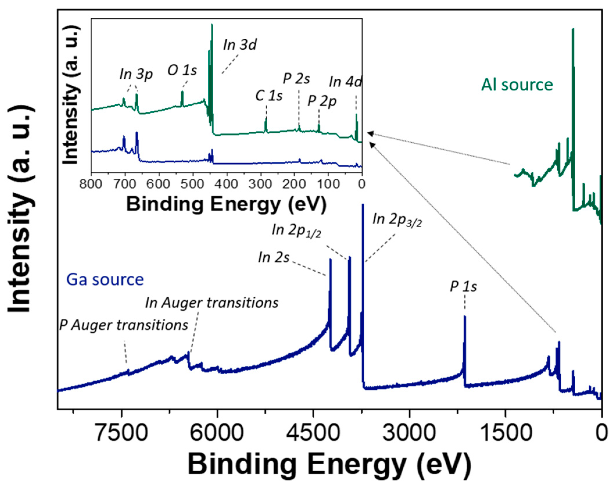
2.4. HAXPES and XPS
3. Results and Discussion
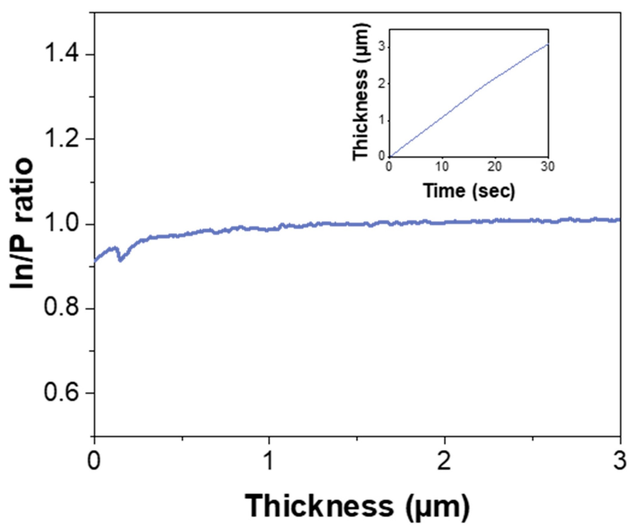
3.1. Pulsed RF GD-OES Profiling of InP
3.2. Analysis Methodology
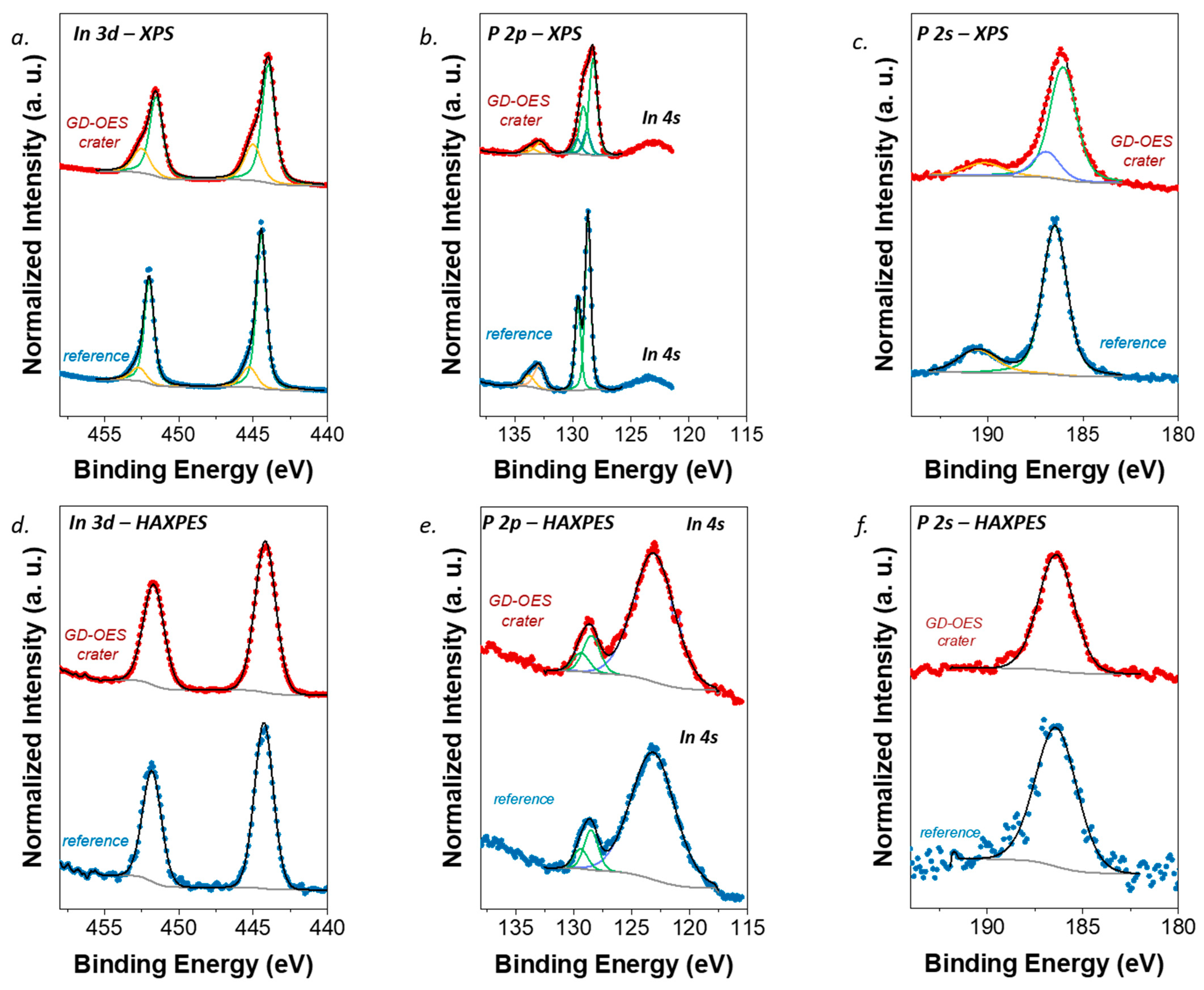
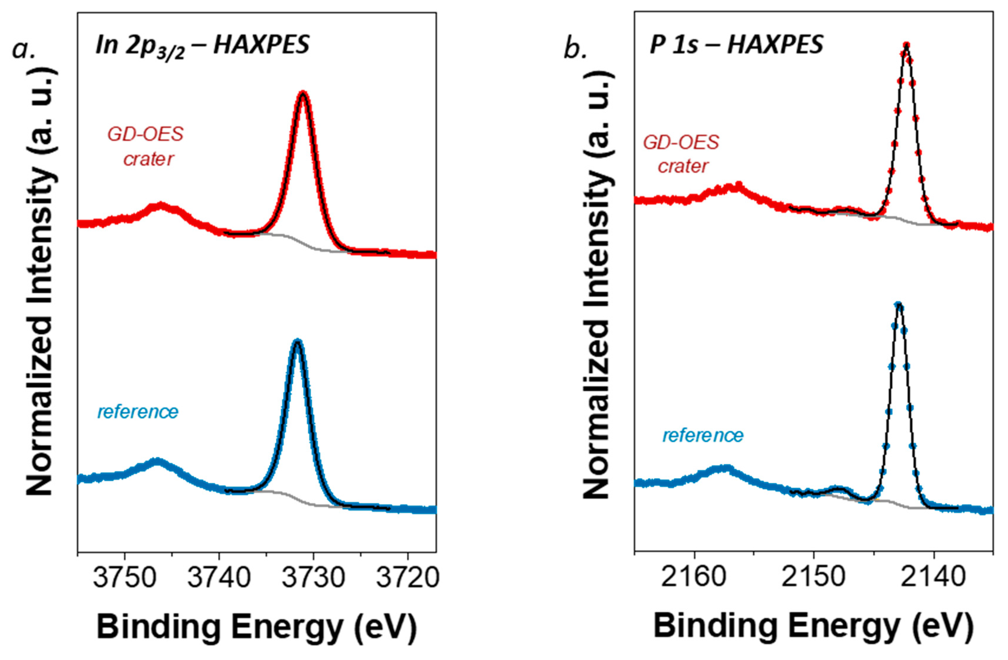
3.3. GD Crater Characterization by Photoemission: XPS vs. HAXPES
4. Conclusions
Supplementary Materials
Author Contributions
Funding
Institutional Review Board Statement
Informed Consent Statement
Data Availability Statement
Conflicts of Interest
References
- Shimizu, K.; Habazaki, H.; Skeldon, P.; Thompson, G.E. Radiofrequency GDOES: A powerful technique for depth profiling analysis of thin films. Surf. Interface Anal. 2003, 35, 564–574. [Google Scholar] [CrossRef]
- Loubat, A.; Bechu, S.; Bouttemy, M.; Eypert, C.; Gaiaschi, S.; Fregnaux, M.; Aureau, D.; Vigneron, J.; Simon, N.; Chapon, P.; et al. Coupling GD-OES and XPS profiling to perform advanced physico-chemical characterizations of III-V layers for photovoltaic applications. In Proceedings of the 2018 IEEE 7th World Conference on Photovoltaic Energy Conversion (WCPEC) (A Joint Conference of 45th IEEE PVSC, 28th PVSEC & 34th EU PVSEC), Waikoloa, HI, USA, 10–15 June 2018. [Google Scholar] [CrossRef]
- Mercier, D.; Bouttemy, M.; Vigneron, J.; Chapon, P.; Etcheberry, A. GD-OES and XPS coupling: A new way for the chemical profiling of photovoltaic absorbers. Appl. Surf. Sci. 2015, 347, 799–807. [Google Scholar] [CrossRef]
- Béchu, S.; Eypert, C.; Loubat, A.; Vigneron, J.; Gaiaschi, S.; Chapon, P.; Bouttemy, M.; Etcheberry, A. Evaluation of the chemical and optical perturbations induced by Ar plasma on InP surface. J. Vac. Sci. Technol. B 2019, 37, 062902. [Google Scholar] [CrossRef]
- Tanuma, S.; Powell, C.J.; Penn, D.R. Calculations of electron inelastic mean free paths. V. Data for 14 organic compounds over the 50-2000 eV range. Surf. Interface Anal. 1994, 21, 165–176. [Google Scholar] [CrossRef]
- Shinotsuka, H.; Tanuma, S.; Powell, C.J.; Penn, D.R. Calculations of electron inelastic mean free paths. X. Data for 41 elemental solids over the 50 eV to 200 keV range with the relativistic full Penn algorithm. Surf. Interface Anal. 2015, 47, 871–888. [Google Scholar] [CrossRef]
- Spencer, B.; Maniyarasu, S.; Reed, B.; Cant, D.; Ahumada-Lazo, R.; Thomas, A.; Muryn, C.; Maschek, M.; Eriksson, S.; Wiell, T.; et al. Inelastic background modelling applied to hard X-ray photoelectron spectroscopy of deeply buried layers: A comparison of synchrotron and lab-based (9.25 keV) measurements. Appl. Surf. Sci. 2021, 541, 148635. [Google Scholar] [CrossRef]
- Renault, O.; Martínez, E.; Zborowski, C.; Mann, J.; Inoue, R.; Newman, J.; Watanabe, K. Analysis of buried interfaces in multilayer device structures with hard XPS (HAXPES) using a CrKα source. Surf. Interface Anal. 2018, 50, 1158–1162. [Google Scholar] [CrossRef]
- Regoutz, A.; Mascheck, M.; Wiell, T.; Eriksson, S.K.; Liljenberg, C.; Tetzner, K.; Williamson, B.A.D.; Scanlon, D.O.; Palmgren, P. A novel laboratory-based hard X-ray photoelectron spectroscopy system. Rev. Sci. Instrum. 2018, 89, 073105. [Google Scholar] [CrossRef] [PubMed]
- Gaiaschi, S.; Richard, S.; Chapon, P.; Acher, O. Real-time depth measurement in glow discharge optical emission spectrometry via differential interferometric profiling. J. Anal. At. Spectrom. 2017, 32, 1798–1804. [Google Scholar] [CrossRef]
- Seah, M.P.; Gilmore, I.S.; Spencer, S.J. Quantitative AES IX and quantitative XPS II: Auger and x-ray photoelectron intensities and sensitivity factors from spectral digital databases reanalysed using a REELS database. Surf. Interface Anal. 2001, 31, 778–795. [Google Scholar] [CrossRef]
- Trzhaskovskaya, M.; Yarzhemsky, V. Dirac–Fock photoionization parameters for HAXPES applications. At. Data Nucl. Data Tables 2018, 119, 99–174. [Google Scholar] [CrossRef]
- Trzhaskovskaya, M.; Yarzhemsky, V. Dirac–Fock photoionization parameters for HAXPES applications, Part II: Inner atomic shells. At. Data Nucl. Data Tables 2019, 129–130, 101280. [Google Scholar] [CrossRef]
- Flament, O.; Druet, E. Calibration of VG ESCALAB MkII spectrometer for XPS quantitative analysis. J. Electron Spectrosc. Relat. Phenom. 1990, 53, 141–152. [Google Scholar] [CrossRef]
- Huschka, W.; Ross, D.; Maier, M.; Umbach, E. Calibrated binding energies of some core levels in the energy range between 1.5–4 keV. J. Electron Spectrosc. Relat. Phenom. 1988, 46, 273–276. [Google Scholar] [CrossRef]
- Franke, R.; Chassé, T.; Streubel, P.; Meisel, A. Auger parameters and relaxation energies of phosphorus in solid compounds. J. Electron Spectrosc. Relat. Phenom. 1991, 56, 381–388. [Google Scholar] [CrossRef]
- Tougaard, S. Practical guide to the use of backgrounds in quantitative XPS. J. Vac. Sci. Technol. A 2021, 39, 011201. [Google Scholar] [CrossRef]
- Wagner, C.D.; Naumkin, A.V.; Kraut-Vass, A.; Allison, J.W.; Powell, C.J.; Rumble, J.R.J. NIST Standard Reference Database 20, Version 3.4. 2003. Available online: http:/srdata.nist.gov/xps (accessed on 25 March 2021).
- Liu, W.K. Preparation of InSb substrates for molecular beam epitaxy. J. Vac. Sci. Technol. B Microelectron. Nanometer Struct. 1995, 13, 1539. [Google Scholar] [CrossRef]


| Photopeak | In 4d | In 4s | P 2p | P 2s | C 1s | In 3d | O 1s | P 1s | Ar 1s | In 2p3/2 |
|---|---|---|---|---|---|---|---|---|---|---|
| Binding Energy (B. E.) (eV) | ~16 | ~122 | ~135 | ~189 | ~285 | ~444 | ~530 | ~2145 | ~3202 | ~3730 |
| Scofield sensitivity factor (Al Kα) | 2.275 | 0.742 | 1.192 | 1.18 | 1.0 | 22.54 | 2.93 | N/A | N/A | N/A |
| Home calculated sensitivity factor (Ga Kα) | 1.75 | 5.95 | 0.54 | 3.13 | 1.0 | 13.0 | 3.45 | 37.8 | 65.2 | 139 |
| Photoionization cross section (9 keV) | 7.842 × 10⁻² | 2.900 × 10⁻¹ | 2.681 × 10⁻² | 1.64 × 10⁻¹ | 5.245 × 10⁻² | 6.655 × 10⁻¹ | 1.863 × 10⁻¹ | 2.469 × 100 | 4.943 × 100 | 1.152 × 101 |
| Photoionization cross section (1.5 keV) | 2.645 × 10⁻¹ | 9.111 × 100 | 1.411 × 10⁻¹ | 1.545 × 10⁻¹ | 1.203 × 10⁻¹ | 2.790 × 10⁻² | 3.583 × 10⁻¹ | N/A | N/A | N/A |
| – | In/P | |||||
|---|---|---|---|---|---|---|
| P 2s–In 3d (XPS) | P 1s–In 2p3/2 (HAXPES) | |||||
| Global | Matrix | Oxide | Global | Matrix | Oxide | |
| InP ref | 1.01 | 1.04 | 0.88 | 1.05 | 1.05 | 0.00 |
| InP GD-OES crater | 1.29 | 1.06 | 2.31 | 1.08 | 1.08 | 0.00 |
Publisher’s Note: MDPI stays neutral with regard to jurisdictional claims in published maps and institutional affiliations. |
© 2021 by the authors. Licensee MDPI, Basel, Switzerland. This article is an open access article distributed under the terms and conditions of the Creative Commons Attribution (CC BY) license (https://creativecommons.org/licenses/by/4.0/).
Share and Cite
Bouttemy, M.; Béchu, S.; Spencer, B.F.; Dally, P.; Chapon, P.; Etcheberry, A. Combined Pulsed RF GD-OES and HAXPES for Quantified Depth Profiling through Coatings. Coatings 2021, 11, 702. https://doi.org/10.3390/coatings11060702
Bouttemy M, Béchu S, Spencer BF, Dally P, Chapon P, Etcheberry A. Combined Pulsed RF GD-OES and HAXPES for Quantified Depth Profiling through Coatings. Coatings. 2021; 11(6):702. https://doi.org/10.3390/coatings11060702
Chicago/Turabian StyleBouttemy, Muriel, Solène Béchu, Ben F. Spencer, Pia Dally, Patrick Chapon, and Arnaud Etcheberry. 2021. "Combined Pulsed RF GD-OES and HAXPES for Quantified Depth Profiling through Coatings" Coatings 11, no. 6: 702. https://doi.org/10.3390/coatings11060702
APA StyleBouttemy, M., Béchu, S., Spencer, B. F., Dally, P., Chapon, P., & Etcheberry, A. (2021). Combined Pulsed RF GD-OES and HAXPES for Quantified Depth Profiling through Coatings. Coatings, 11(6), 702. https://doi.org/10.3390/coatings11060702