Abstract
In this study, nitrogen-vacancy center emissions from nanocone structures fabricated on diamond surfaces by gold film annealing and inductively coupled plasma etching techniques were characterized. First, the diamond substate deposited with gold film was annealed to form a nano-sized dot mask. Second, through inductively coupled plasma etching, nanocone-shaped structures were fabricated using optimized gold dots as masks. Finally, the as-fabricated nanocone and planar structures were investigated with photoluminescence experiments at temperatures ranging from room temperature to 80 K, with the results showing approximately two-fold higher emission values for nitrogen-vacancy centers from nanocones.
1. Introduction
In recent years, optically active impurities in diamond—so-called color centers–have attracted intense research interest. Their unique properties, which include highly stable fluorescence (photostability) at room temperature and feasible control of highly coherent spinning associated with color centers, give them potential in various applications [1,2]. More than 500 different diamond color centers are known [3], and their emission wavelengths span a spectral range from the ultraviolet to the near infrared. Furthermore, the diamond host material possesses outstanding properties, including chemical inertness, biocompatibility, high transparency from the ultraviolet to infrared spectral range, as well as a high mechanical strength and high thermal conductivity [4,5,6]. Hence, color centers in diamonds have to be considered as potential building blocks of future quantum information processing architectures and integrated nanophotonic devices [7,8]. Among these color centers, the nitrogen-vacancy (N-V) centers have a more stable coherent time (T2 = 1.8 ms) [9] and are easily manipulated and controlled with electromagnetic fields [10], making them more attractive. So far, the N-V centers in diamond have been identified as excellent candidates for long-distance quantum communication, quantum computation, and nanoscale detection of temperature and magnetic or electric fields [11,12,13,14,15,16,17]. Efforts to improve the emissions of color centers in diamond have involved micro- or nanostructures on diamond surfaces. For instance, the emission efficiencies of N-V or other centers have been improved with nanowire, nanopillar, nanotaper, microcavity, nanolens, and hybrid nanopit nanostructures. [18,19,20,21,22].
To date, diamond nanostructures have been fabricated via different routines. Nanopits were fabricated by annealing diamond with gold particles [23]. With hard masks such as gold dots or nanodiamond particles, nanopillars and nanowires can be achieved via inductively coupled plasma (ICP) etching [24,25,26]. Nanopillars were also constructed on a nanodiamond film surface by bias-assisted reactive ion etching in hydrogen–argon microwave plasma [27]. In addition, some microstructures of solid immersion lenses were fabricated to increase the emission of N-V centers with a focused ion beam [28]. However, nanostructures measuring 100 nm or even smaller on single crystal diamonds have rarely been reported. In this work, nanocones measuring 26 nm and with narrow size distribution were fabricated by ICP etching using gold dot masks to achieve high emission diamond N-V centers. The photoluminescence (PL) properties of diamonds with nanocone and planar structures were characterized at temperatures ranging from room temperature to 80 K.
2. Experimental Procedure
2.1. Fabrication
The substrate used in this work was a chemical vapor-deposited (001) diamond measuring 3 × 3 × 0.5 mm3. N-V centers were prepared with nitrogen doping during the diamond growth process. Firstly, the substrate was dipped into a mixed acid of H2SO4:HNO3:HClO4 (volume ratio: 31.2:36:11.4) at 250 °C for 1 h and a mixed alkali of NH4OH:H2O2:H2O (volume ratio: 4:3:9) at 80 °C for 10 min to remove the non-diamond phase. Secondly, the implanted layer was epitaxially grown on the as-washed substrate using microwave plasma chemical vapor deposition equipment (AX6500 Seki Technotron Corporation, Tokyo, Japan). During growth, the typical growth parameters were as follows: a total gas pressure of 100 Torr, a H2 gas flow rate of 500 sccm, a N2/CH4 ratio of 4.3 ppm. The growth time was 10 h and the thickness of the implanted layer was estimated to be 100 µm. Details of the growth conditions are presented in Table 1. The layer was expected to result in a uniform N distribution in the substrate. The density of N in the as-grown diamond was about 1016 cm−3, while the 2D density was deduced to be 1014 cm−2. The as-grown diamond was polished on the growth side and laser-cut into several small samples. After the above processes, nanostructures were prepared on each sample. Figure 1 shows the fabrication flow chart for nanostructures. Gold films with thicknesses ranging from 2 to 40 nm were deposited on diamond by electron beam evaporation. Then, the samples were held in a furnace for annealing at the desired temperature for various times to achieve well-distributed gold dot masks. The Ar gas was introduced into the furnace to avoid sample oxidation. After annealing, gold dot masks were obtained.

Table 1.
Details of experimental conditions of diamond growth with N doping.
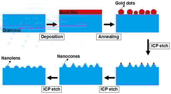
Figure 1.
Schematic of fabrication of nanostructures on diamond surface. ICP, inductively coupled plasma.
Finally, the diamonds with optimized gold masks were etched with an ICP etching system (Oxford, ICP-180, Oxford, England) to obtain nanostructures. Here, O2 gas was used for etching gas with a flow rate of 50 sccm. The chamber pressure, coil power, and bias voltage were 10 mTorr, 450 W, and 130 V, respectively. During the etching process, a low radio frequency power was utilized to obtain a smooth surface on the diamonds [29]. The etching time ranged from 5 s to 3 min. After ICP etching, the samples were washed in hydrochloric and nitric acids at a volume ratio of 3:1 to remove the remaining gold.
2.2. Sample Characterization
The morphologies of the metal mask and the fabricated diamond nanostructures were characterized by scanning electron microscopy (SEM) (Quanta, F-250, Waltham, MA, USA). In order to give a three-dimensional perspective, the sample was mounted at a 45° angle to the stage. The optical properties of the diamond nanostructures were investigated using photoluminescence spectra excited with a continuous wave in the 532 nm wavelength. The raw laser power was 100 mW; since a neutral density filter with a value of 1% was utilized, the power of the laser reaching sample surface was about 1 mW. The magnification of the objective was 50×, resulting in a laser spot size of about 2 µm. The temperature ranged from room temperature to 80 K, with cooling intervals of 10 K. Before the sample was measured, it was kept at each fixed temperature for 3 min.
3. Results and Discussion
By annealing nanoscale-thickness gold film, the film dewetted and self-assembled into dots. To achieve a well-distributed nano-sized gold dot mask, the gold films of different thicknesses were annealed at different temperatures on the diamond surfaces. Gold films with a thickness of about 3 nm were respectively annealed at 600, 800, and 1100 °C for 5 min, the results of which are shown in Figure 2b–d. Before annealing, the film was discontinuous due to its very thin thickness, as shown in Figure 2a. When the annealing temperature was 600 °C, separated and irregularly shaped gold islands were formed. With continued increase of the temperature to 800 °C, nearly circle-shaped gold dots were achieved. When the temperature reached 1100 °C, relatively larger gold dots were observed and the spaces between dots became larger.
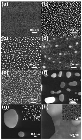
Figure 2.
SEM images of gold masks with different annealing temperatures and thicknesses: (a) initial as-deposited gold film with a thickness of about 3 nm; (b–d) sample with gold film shown in (a) after sequentially annealing at 600, 800, and 1100 °C for 5 min; (e,f) samples with initial gold film thicknesses of 3, 10, 20, and 40 nm after sequentially annealing at 800 °C for 5 min. Insets show (g,h) at low magnification, respectively.
In the second experiment, gold films with thicknesses of 3, 10, 20, and 40 nm were annealed at 800 °C for 5 min, the results of which are shown in Figure 2e–h, respectively. From the results, the size of the gold dots increased with the increasing film thickness. When the thickness was above 10 nm, the shape of the gold dots became irregular and partially continuous, as shown in the inset in Figure 2g,h, respectively. The temperature-dependent phenomenon could be because the dewetted gold dots melted and converged together into larger dots with the increasing annealing temperature. Meanwhile, the thickness dependence results may be ascribed to the sizes of the initial nucleation points, which were dependent on the film thickness, determining the final shape of the dewetted dots. Since the dots used in one popular work study gold spheres rather than a thin film [30], the mask thickness was thicker, resulting in a better etching resistance for such a small size structure.
To obtain nanostructures with well-distributed sizes on diamond surfaces, the gold dots in Figure 2e were chosen as masks in the next ICP etching process. In this process, one 3 × 3 mm2 diamond substrate was cut into four 1.5 × 1.5 mm2 substrates. One of these was a blank sample for comparison. The same gold dot mask was prepared on the other substrates. Then, the samples with gold dot masks were ICP-etched for various time periods. Figure 3 shows SEM images of the initial masked sample and the samples etched for 30, 60, and 90 s in tilt angle view. The nanostructures of samples etched for 30 s exhibit well-arranged nanocone morphologies. As shown in the inset of Figure 3b, these nanocones have a narrow size distribution range of 9.58 to 41.3 nm, and their average size was evaluated to be about 26 nm. The average height of the nanocones was evaluated to be 27.6 nm. With extended etching time, the morphologies of the nanostructures changed to an almost nanolens shape. The cone shape was formed because of the relatively high selectivity ratio between the etching rates of diamond and gold. With further etching, the top of cone, which is more chemically active to oxygen plasma, was etched faster than other part of cone, leading to the blunt lens shape.
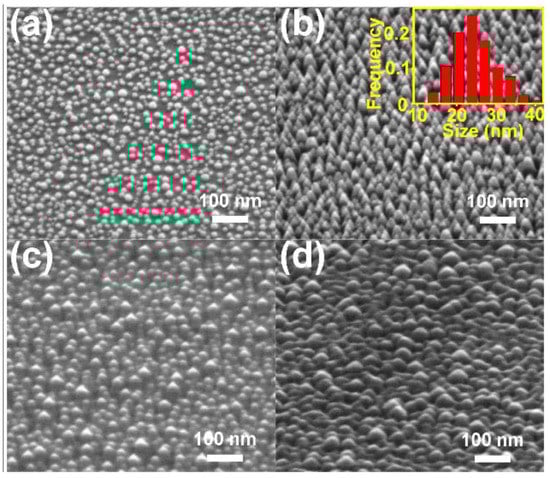
Figure 3.
SEM images of sample with gold masks (a) before and (b–d) after inductively coupled plasma (ICP) etching for 30, 60, and 90 s, respectively. Inset: size distribution histogram of nanocones in (b).
The PL experiment was carried out to investigate the emission efficiency of the N-V center ensemble in diamonds with planar and nanocone structures. Results ranging from room temperature to 80 K were obtained and are shown in Figure 4a,b, respectively. As seen in the results, the PL intensities of all peaks were increased with decreasing temperature. This was mainly due to that the lattice vibration of the diamond being reduced with decreasing temperature, which resulted in a highlighted PL signal. Meanwhile, the peaks for N-V0 and N-V− shifted with various temperatures. Since the intensity of the lattice vibration in a diamond relies on the amount of diamond atoms, PL signals can be normalized in accordance with the diamond’s characteristic peak in the same experimental conditions. Hence, all spectra were normalized using the intensity of the diamond’s atomic vibration peak. Following normalization lines, baseline corrections were performed with 8 baseline points using the end-weighted method. These results are shown in the insets of Figure 4a,b, respectively. Obviously, from the normalized results, both the N-V0 and N-V− emission intensities of nanocone samples are higher than that of the planar sample in the entire temperature region, suggesting enhanced features of nanostructures on diamond surfaces.
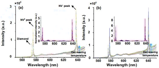
Figure 4.
Photoluminescence spectra of samples with (a) planar and (b) nanocone surfaces range from room temperature to 80 K, respectively. Insets: normalized and baseline spectra of planar and nanocone samples, respectively.
In order to give a clear view, two peaks for N-V0 and N-V− were magnified by cutting the spectra ranged from 579 to 634 nm, which did not affect the analysis of these two peaks, as shown in Figure 5a,b, respectively. The emission intensities at each temperature point were sampled out from these two results and are shown in Figure 5c,d. The emission intensities of N-V0 and N-V− decreased with increasing temperature and the degree of enhancement had a slight decreasing tendency with increasing temperature, which may be ascribed to the lower signal-to-noise ratio caused by phonon vibration interference at high temperature.

Figure 5.
Normalized and baseline corrected, magnified photoluminescence spectra of samples with (a) planar and (b) nanocone surfaces range from room temperature to 80 K, respectively. The peak areas for (c) N-V0 and (d) N-V− changed as the temperature cooled.
Upon cooling, all PL spectra showed enhanced N-V center ensemble emissions with nanostructures. The enhancement could be because the nanostructure geometry allows for high emission and collection efficiencies [18].
The N-V emission from nanocones was improved by 1.8 times compared to the collection from the planar diamond, which may be lower than for the single N-V center sample. The difference may stem from the interference between color centers. In the work of [18], a nanopillar was used to increase the single color center and two neighboring single color centers had enough space to avoid interference with each other. Since a nanocone has multiple N-V centers with random dipole orientations, this results in phase interference between photons, which is a reason for lower collection and enhancement efficiencies [20,31]. Additionally, the nanocone sample had a larger surface area than the planar sample, which may be another reason for the improvement. This is because these nanocones may condense the incident light to increase the PL intensity further [22].
Upon cooling, peak shifts and broadening of both N-V0 and N-V− were observed in these spectra. In order to gain deep insight into the N-V center emissions in planar and nanocone diamonds, the peak position shifts and widths of N-V0 and N-V− ensembles at different temperatures were investigated, as shown in Figure 6. Two charged state N-V centers had similar temperature dependence behaviors. Since the peak position is related to the electronic transition, the nm position unit was transformed to an eV energy unit. From the position shift results, it can be seen that the N-V0 and N-V− positions redshifted with increasing temperature. The shrinkage of emission peak redshifts from 80 K to room temperature equaled 1.956 and 3.036 meV for N-V0 and N-V− centers, respectively, which were close to the results from previous work [32]. It is thought that the redshift is related to the narrowing of the diamond bandgap. In diamond, the temperature dependence of the bandgap, Eg (T), can be described by the following empirical relation [33]:
where Eg (0) is the value of the gap at 0 K and α and β are constants. Therefore, going from 0 to 300 K, the bandgap of the diamond decreased by about 15.7 meV, which was much larger than the redshift of 3.03 and 1.95 meV from the N-V centers in present work. When the bandgap shrinks, concomitant reductions in the separation energy between the ground state (located inside the gap) of 1.9 and 2.1 eV in the centers and associated band edges are expected [34]. Hizhnyakov took the softening of the elastic spring in the excited state into consideration when explaining the temperature broadening and shifting of N-V centers in diamonds [35]. From the theory in Hizhnyakov’s work, the shift and width changes with temperature followed the T2-T4 and T3-T7 laws, respectively. The related equations are shown below:
where δ and γ are the contributions of quadratic vibronic interaction to the N-V center’s frequency and width, respectively; µ, ν, a, and b are constant. We used those two laws to verify the shift and width changes of N-V0 and N-V− emissions by fitting the experimental data with Equations (2) and (3), respectively, showing well-fitted results.
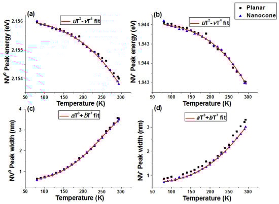
Figure 6.
Photo energy and peak width of N-V0 (a,c) and N-V− (b,d) peaks at various temperatures. The redlines are fitting data for N-V center peak energy and width, respectively.
The closeness of the results for planar and nanocone samples was due to the fact that two results originated from the same diamond substrate. In comparison with the plasmon resonance-enhanced emission of Si-V centers [22], our results also suggest that the nanocone structure improves the emission efficiency, with no other electronic state changes. Hence, we expect that these nanostructures will be used to improve the N-V center emission in nanothermometry or maser devices.
4. Conclusions
In this paper, nanocones were obtained on diamond surface using thermal annealing of thin gold films and ICP etching. A gold dot mask with a narrow distributed size was obtained by optimizing the annealing temperature and the gold film’s thickness. Well-arranged nanocones measuring 26 nm were fabricated with an etching time of 30 s in the ICP etching process. The temperature dependence of N-V center emissions from as-fabricated nanocones and planar structures was studied, demonstrating that the nanocone structures play a role in increasing the emission intensity. Our results are also coincident with the theoretical model of elastic spring softening of N-V centers in the electronic transition with increasing temperature.
Author Contributions
Conceptualization, T.Z. and H.W.; methodology, T.Z.; formal analysis, Y.L., Z.L., J.F., and J.W.; investigation, R.W., and Q.W.; data curation, Y.W., D.Z., and G.S.; writing—original draft preparation, T.Z.; writing—review and editing, T.Z.; supervision, T.M.; project administration, H.W.; funding acquisition, T.Z., F.W., W.W., and H.W. All authors have read and agreed to the published version of the manuscript.
Funding
This work was supported by the Fundamental Research Funds for the Central Universities (xpt012020005), National Key R&D Program of China (2017YFB0402800), National Natural Science Foundation of China (NSFC) (61705176, 61627812 and 61605155), Natural Science Fund of Shaanxi Province (No. 2018JQ6002), China Postdoctoral Science Foundation (2018T111057) and Dongguan Introduction Program of Leading Innovative and Entrepreneurial Talents.
Acknowledgments
The authors are thankful to Yanzhu Dai from the International Center for Dielectric Research (ICDR), Xi’an Jiaotong University, for her help in using SEM; and Jicheng Li from the State Key Laboratory for Manufacturing Systems Engineering, Xi’an Jiaotong University, for his help with ICP experiments. Tian-fei Zhu thanks his wife and son for their supports and encouragement.
Conflicts of Interest
The authors declare no conflict of interest.
References
- Kurtsiefer, C.; Mayer, S.; Zarda, P.; Weinfurter, H. Stable solid-state source of single photons. Phys. Rev. Lett. 2000, 85, 290–293. [Google Scholar] [CrossRef] [PubMed]
- Eisaman, M.D.; Fan, J.; Migdall, A.; Polyakov, S.V. Invited review article: Single-photon sources and detectors. Rev. Sci. Instrum. 2011, 82, 71101. [Google Scholar] [CrossRef]
- Zaitsev, A. Optical Properties of a Diamond; Springer: Berlin, Germany, 2001. [Google Scholar]
- Wort, C.J.; Balmer, R.S. Diamond as an electronic material. Mater. Today 2008, 11, 22–28. [Google Scholar] [CrossRef]
- Mochalin, V.N.; Shenderova, O.; Ho, D.; Gogotsi, Y. The properties and applications of nanodiamonds. Nat. Nanotechnol. 2011, 7, 11–23. [Google Scholar] [CrossRef] [PubMed]
- Krueger, A. Diamond nanoparticles: Jewels for chemistry and physics. Adv. Mater. 2008, 20, 2445–2449. [Google Scholar] [CrossRef]
- Aharonovich, I.; Neu, E. Diamond nanophotonics. Adv. Opt. Mater. 2014, 2, 911–928. [Google Scholar] [CrossRef]
- Schirhagl, R.; Chang, K.; Loretz, M.; Degen, C.L. Nitrogen-vacancy centers in diamond: Nanoscale sensors for physics and biology. Annu. Rev. Phys. Chem. 2014, 65, 83–105. [Google Scholar] [CrossRef]
- Balasubramanian, G.; Neumann, P.; Twitchen, D.; Markham, M.; Kolesov, R.; Mizuochi, N.; Isoya, J.; Achard, J.; Beck, J.; Tissler, J.; et al. Ultralong spin coherence time in isotopically engineered diamond. Nat. Mater. 2009, 8, 383–387. [Google Scholar] [CrossRef]
- Doherty, M.W.; Manson, N.B.; Delaney, P.; Jelezko, F.; Wrachtrup, J.; Hollenberg, L.C.L. The nitrogen-vacancy colour centre in diamond. Phys. Rep. 2013, 528, 1–45. [Google Scholar] [CrossRef]
- Childress, L.; Taylor, J.M.; Lukin, M.D.; Sørensen, A.S. Fault-tolerant quantum communication based on solid-state photon emitters. Phys. Rev. Lett. 2006, 96, 070504. [Google Scholar] [CrossRef]
- Jelezko, F.; Gaebel, T.; Popa, I.; Gruber, A.; Wrachtrup, J. Observation of coherent oscillations in a single electron spin. Phys. Rev. Lett. 2004, 92, 076401. [Google Scholar] [CrossRef]
- Li, X.Q.; Zhao, Y.F.; Tang, Y.N.; Yang, W.J. Entanglement of quantum node based on hybrid system of diamond nitrogen-vacancy center spin ensembles and superconducting quantum circuits. Acta Phys. Sin. 2018, 67, 070302. [Google Scholar]
- Ozawa, H.; Tahara, K.; Ishiwata, H.; Hatano, M.; Iwasaki, T. Formation of perfectly aligned nitrogen-vacancy-center ensembles in chemical-vapor-deposition-grown diamond (111). Appl. Phys. Express 2017, 10, 45501. [Google Scholar] [CrossRef]
- Wang, J.; Feng, F.; Zhang, J.; Chen, J.; Zheng, Z.; Guo, L.; Zhang, W.; Song, X.; Guo, G.-P.; Fan, L.; et al. High-sensitivity temperature sensing using an implanted single nitrogen-vacancy center array in diamond. Phys. Rev. B 2015, 91, 155404. [Google Scholar] [CrossRef]
- Zhang, C.; Yuan, H.; Zhang, N.; Xu, L.X.; Li, B.; Cheng, G.D.; Wang, Y.; Gui, Q.; Fang, J.C. Dependence of high density nitrogen-vacancy center ensemble coherence on electron irradiation doses and annealing time. J. Phys. D Appl. Phys. 2017, 50, 505104. [Google Scholar] [CrossRef]
- Ahmadi, S.; El-Ella, H.A.R.; Wojciechowski, A.M.; Gehring, T.; Hansen, J.O.B.; Huck, A.; Andersen, U.L. Nitrogen-vacancy ensemble magnetometry based on pump absorption. Phys. Rev. B 2018, 97, 24105. [Google Scholar] [CrossRef]
- Babinec, T.M.; Hausmann, B.J.M.; Khan, M.; Zhang, Y.; Maze, J.; Hemmer, P.R.; Lončar, M. A diamond nanowire single-photon source. Nat. Nanotechnol. 2010, 5, 195–199. [Google Scholar] [CrossRef]
- Xie, L.; Zhou, T.; Stöhr, R.J.; Yacoby, A. Crystallographic orientation dependent reactive ion etching in single crystal diamond. Adv. Mater. 2018, 30, 1705501. [Google Scholar] [CrossRef]
- Barclay, P.E.; Santori, C.; Fu, K.-M.; Beausoleil, R.G.; Painter, O. Coherent interference effects in a nano-assembled diamond NV center cavity-QED system. Opt. Express 2009, 17, 8081–8197. [Google Scholar] [CrossRef]
- Liu, Z.; Abbasi, H.N.; Zhu, T.-F.; Wang, Y.-F.; Fu, J.; Wen, F.; Wang, W.; Fan, S.; Wang, K.; Wang, H.-X. Fabrication of micro lens array on diamond surface. AIP Adv. 2019, 9, 125218. [Google Scholar] [CrossRef]
- Cheng, S.; Song, J.; Wang, Q.; Liu, J.; Li, H.; Zhang, B. Plasmon resonance enhanced temperature-dependent photoluminescence of Si-V centers in diamond. Appl. Phys. Lett. 2015, 107, 211905. [Google Scholar] [CrossRef]
- Song, J.; Li, H.; Lin, F.; Wang, L.; Wu, H.; Yang, Y. Plasmon-enhanced photoluminescence of Si-V centers in diamond from a nanoassembled metal–diamond hybrid structure. CrystEngComm 2014, 16, 8356. [Google Scholar] [CrossRef]
- Yang, N.; Uetsuka, H.; Osawa, E.; Nebel, C.E. Vertically aligned nanowires from boron-doped diamond. Nano Lett. 2008, 8, 3572–3576. [Google Scholar] [CrossRef]
- Janssen, W.; Gheeraert, E. Dry etching of diamond nanowires using self-organized metal droplet masks. Diam. Relat. Mater. 2011, 20, 389–394. [Google Scholar] [CrossRef]
- Smirnov, W.; Kriele, A.; Yang, N.; Nebel, C. Aligned diamond nano-wires: Fabrication and characterisation for advanced applications in bio- and electrochemistry. Diam. Relat. Mater. 2010, 19, 186–189. [Google Scholar] [CrossRef]
- Zou, Y.S.; Yang, Y.; Zhang, Y.-L.; Chong, Y.M.; He, B.; Bello, I.; Lee, S.T. Fabrication of diamond nanopillars and their arrays. Appl. Phys. Lett. 2008, 92, 53105. [Google Scholar] [CrossRef]
- Jamali, M.; Gerhardt, I.; Rezai, M.; Frenner, K.; Fedder, H.; Wrachtrup, J. Microscopic diamond Solid-Immersion-Lenses fabricated around single defect ceneters by focussed ion beam milling. Rev. Sci. Instrum. 2014, 85, 123703. [Google Scholar] [CrossRef]
- Zhu, T.-F.; Fu, J.; Wang, W.; Wen, F.; Zhang, J.; Bu, R.; Ma, M.; Wang, H.-X. Fabrication of diamond microlenses by chemical reflow method. Opt. Express 2017, 25, 1185–1192. [Google Scholar] [CrossRef]
- Hausmann, B.J.; Khan, M.; Zhang, Y.; Babinec, T.M.; Martinick, K.; McCutcheon, M.; Hemmer, P.R.; Lončar, M. Fabrication of diamond nanowires for quantum information processing applications. Diam. Relat. Mater. 2010, 19, 621–629. [Google Scholar] [CrossRef]
- Liu, S.; Li, J.; Yu, R.; Wu, Y. Achieving maximum entanglement between two nitrogen-vacancy centers coupling to a whispering-gallery-mode microresonator. Opt. Express 2013, 21, 3501–3515. [Google Scholar] [CrossRef]
- Chen, X.-D.; Dong, C.-H.; Sun, F.-W.; Zou, C.-L.; Cui, J.-M.; Han, Z.-F.; Guo, G.-C. Temperature dependent energy level shifts of nitrogen-vacancy centers in diamond. Appl. Phys. Lett. 2011, 99, 161903. [Google Scholar] [CrossRef]
- Varshni, Y. Temperature dependence of the energy gap in semiconductors. Physica 1967, 34, 149–154. [Google Scholar] [CrossRef]
- Feng, T.; Schwartz, B.D. Characteristics and origin of the 1.681 eV luminescence center in chemical-vapor-deposited diamond films. J. Appl. Phys. 1993, 73, 1415–1425. [Google Scholar] [CrossRef]
- Hizhnyakov, V.; Kaasik, H.; Sildos, I. Zero-phonon lines: The effect of a strong softening of elastic springs in the excited state. Phys. Status Solidi 2002, 234, 644–653. [Google Scholar] [CrossRef]
© 2020 by the authors. Licensee MDPI, Basel, Switzerland. This article is an open access article distributed under the terms and conditions of the Creative Commons Attribution (CC BY) license (http://creativecommons.org/licenses/by/4.0/).