Abstract
Lead halide perovskites (LHPs) have superior luminescent properties, but their toxicity hinders their commercialization, arousing interests in tin halide perovskites as environmentally friendly substitutes for LHPs. Herein, we synthesized a series of two-dimensional tin halide perovskite ODASnBr4-xIx (ODA denotes 1,8-octanediammonium, X = 0, 1, 2, 3, 4) microcrystals via an aqueous-phase method. The differences between ODASnI4 and ODASnBr4 in luminescent properties and morphological characteristics were systematically discussed for the first time and attributed to light-driven ligand-to-metal charge transfer. The prepared ODASnBr4 has a PL peak at 567 nm and a PL QY of 99%, and the white light-emitting diodes fabricated with ODASnBr4 and commercial blue phosphors realized a luminous efficacy of up to 96.27 lm/W, which demonstrated the remarkable potential of ODASnBr4 microcrystals for high-efficiency white light-emitting diode applications.
1. Introduction
Lead halide perovskites (LHPs) have been widely studied in this century due to their significant luminescent properties, including high color purity, tunable bandgap, and high photoluminescence quantum yield (PL QY), demonstrating promising prospects in fields such as electroluminescence [1,2,3,4,5,6], solar cells [7,8], photodetectors [9], and bioimaging [10]. However, the severe biotoxicity of lead impedes the commercialization of LHPs. Tin is an element of Group IVA and is analogous to lead. As the degradation products of tin halide perovskites (THPs) are mostly low-toxic, such as tin oxides and tin halides, extensive studies have been inspired on THPs as eco-friendly alternatives to LHPs in recent years.
In contrast to conventional band-edge-to-band-edge emission, some two-dimensional (2D) THPs exhibit a distinct luminescent behavior known as self-trapped exciton (STE) emission [11]. Such luminescent behavior originates from localized excitons induced by lattice distortion, which typically requires the coexistence of low lattice deformation energy and strong exciton–phonon coupling [12]. Consequently, STE emission is mainly observed in zero-dimensional perovskites, whereas in 2D THPs, such emission has only been reported in perovskites incorporating specific A-site cations. STE emission usually exhibits a PL spectrum with wide full width at half maximum (FWHM) and high PL QY. Wang et al. first reported the synthesis of OA2SnX4 (OA denotes octylammonium, X = Br, I) in acidic aqueous solution [13]. The prepared microcrystal has a PL QY as high as 95% and a broadband spectrum covering yellow and red spectrum regions. Li et al. presented an air ambient method for the synthesis of 2D THP (RNH3)2+xSnI4+x [14]. The PL QY of HA2SnI4 (HA denotes hexylammonium) was increased from less than 1% to 99% (HA2+xSnI4+x), and the white light-emitting diodes (WLEDs) fabricated with HA2+xSnI4+x had Commission Internationale de l’Eclairage (CIE) coordinates at (0.447, 0.383), a correlated color temperature (CCT) of 2654 K, and a high color rendering index (CRI) of 92. Chen et al. discussed the effect of exciton localization on enhancing STE emission in 2D THPs [15]. They proposed a facile vacancy tuning strategy by changing the feeding ratio of amine and tin precursors. The PL QY of OA2SnI4 increased from approximately 1% to 63.6%, which was one of the best records in tin iodide perovskites. Recent reports on 2D THPs with STE emission are summarized in Table 1. As one of the most studied A-site cations, 1,8-octanediammonium (ODA2+) can naturally induce STE emission in 2D THPs. In addition, some previous reports demonstrated the outstanding optical properties of ODASnBr4. However, as an emerging material, ODASnBr4 has not been widely explored for its potential in WLED applications.

Table 1.
Summary of recent reports on STE-emitting 2D THPs.
Furthermore, experiments have demonstrated that halogen ions can also impact the formation of STE emission. Chen et al. synthesized halogen-ion-tunable PEA2SnX4 (PEA denotes phenylethylammonium, X = Br, I), whose FWHM can be widened from 36 nm (PEA2SnI4) to 80 nm (PEA2SnBr4) [24]. Yao et al. synthesized TMPDA2SnX4 (X = Cl, Br, I; TMPDA denotes N,N,N′,N′-tetramethyl-1,4-phenylenediammonium) [25]. Interestingly, TMPDA2SnI4 and TMPDA2SnBr4 were both narrowband-emitting 2D THPs, but TMPDA2SnCl4 naturally formed a one-dimensional five-coordinated pyramid configuration and exhibited STE emission, which was attributed to the long Sn···Cl bond. Notably, studies have revealed that in metal halide perovskites, I− ions exhibit significantly stronger suppression of lattice distortion compared to Br− ions and Cl− ions, which is in line with their bigger ionic radius [26]. Therefore, STE emission in tin–iodide perovskites is comparatively rare. In addition, the larger ionic radius of I− ions compared to Br− ions makes it easier to be oxidized [27,28], resulting in the formation of tin vacancies and a low PL QY in tin iodide perovskites.
Herein, an aqueous-phase method was employed for the synthesis of STE-emitting DJ phase ODASnBr4−xIx microcrystals. Effects of different halogen ions on the optical properties of the perovskite are confirmed via X-ray photoelectron spectroscopy (XPS) and Fourier-transform infrared spectroscopy (FTIR) characterization, and it turns out that bi-oxidation of Sn2+ and I− is the cause of the low PL QY in ODASnI4 perovskites. The prepared ODASnBr4 microcrystal exhibits a broadband emission peak at 567 nm (FWHM~114 nm) with a near-unity PL QY and remarkable stability. Finally, a series of WLEDs with tunable correlated color temperature (CCT) are prepared by encapsulating ODASnBr4 and commercially available blue phosphor on a 365 nm ultraviolet (UV) chip under different blending ratios, with a luminous efficacy (LE) up to 96.27 lm/W.
2. Materials and Methods
2.1. Materials
Stannous oxide (SnO, 99.9%), hypophosphorous acid (H3PO2, 50%), hydroiodic acid (HI, 55–58%), hydrobromic acid (HBr, 48%), octylenediamine (C8H20N2, 98%), tin(II) bromide (SnBr2, 99%), stannous oxalate (SnC2O4, 98%), and stannous octoate (C16H30O4Sn, 95%) are purchased from Aladdin (Waukesha, WI, USA). Ethyl acetate (C4H8O2, AR) is purchased from Sinopharm (Beijing, China). All chemicals are used without purification unless otherwise noted.
2.2. Synthesis of ODASnI4 Perovskite Microcrystals
For the synthesis of ODASnI4 microcrystals, SnO (0.1347 g), ODA (0.1731 g), HI solution (4 mL), and H3PO2 solution (13.5 mL) are added into a 100 mL flat-bottomed glass beaker and stirred at 600 rpm in order that the precursors can dissolve completely. Subsequently, the solution is heated from room temperature to 100 °C within 5 min and maintained at this temperature for 30 min. After that, the solution is allowed to cool down naturally and is ultrasonically treated for 10 min to facilitate the crystallization of ODASnI4 microcrystals.
2.3. Synthesis of ODASnBr4−xIx Perovskite Microcrystals
The synthesis of ODASnBr4−xIx microcrystals is similar to that of ODASnI4, except that HI solution in the precursor is replaced with HBr solution. For x = 1, 2, 3, 4, the HBr solution and HI solution used are (4 − x) mL and x mL, respectively.
2.4. Preparation of ODASnI4-BMA WLED
For the preparation of ODASnI4-BMA WLED, the phosphor, Part A glue (Epoxy resin) and Part B glue (Hardener) are uniformly mixed at a mass ratio of 20:1:4 and then encapsulated onto a 365 nm UV chip and cured under UV light for one hour. The phosphor is composed of ODASnBr4 microcrystals and commercially available BaMg2Al16O27:Eu2+ (BMA) phosphor blended at different mass ratios.
2.5. Characterization
Photoluminescence (PL) spectra and photoluminescence excitation (PLE) spectra of the prepared 2D THP microcrystals are recorded using an F97XP fluorescence spectrophotometer. Time-resolved photoluminescence (TRPL) decay curves of the perovskite powders are recorded using an FLS920 spectrophotometer. Chemical valence state and concentration of each element are determined by an Escalab Xi+, Thermo Fisher (Waltham, MA, USA), with a minimum resolution of 0.1 eV. The binding energy calibration is based on C 1s at 284.8 eV. The X-ray diffraction (XRD) patterns of the 2D THPs were recorded using a D8VENTURE MetalJet X-ray diffractometer equipped with Cu K α radiation (k = 1.54178 Å), with the voltage and current set to 40 kV and 40 mA, respectively. The morphology of the powder 2D THPs and element mapping images are obtained using an S4800 scanning electron microscope (SEM) operating at 15.0 kV. The diffuse reflectance spectra of perovskite microcrystals are recorded using a PE Lambda 750. The FTIR spectroscopy is recorded by using Nicolet Summit X (Thermo Fisher, Waltham, MA, USA). Photographs are taken by using the Vivo Neo 10.
3. Results and Discussion
The large size of iodide ions inhibits the deformation of the inorganic layer as well as the appearance of STEs. Therefore, there are few relevant reports of 2D tin–iodide perovskites exhibiting STE emission. Considering that the soft straight-chain structure of long-chain aliphatic organic molecules promotes the localization of excitons, we choose ODA2+, a kind of bivalent amine, as the A-site cation of the target DJ-phase 2D THP. The amine group of ODASnI4 is connected with the halogen ions by hydrogen bonding, which results in a shorter interlayer spacing as well as better stability of the perovskite compared to RP-phase 2D perovskites such as OA2SnI4 [15].
Using an aqueous-phase method, the microcrystalline 2D THP ODASnBr4-xIx (x denotes the amount of hydrohalic acid in the precursor, x = 0, 1, 2, 3, 4) were successfully synthesized by gradually adjusting the type of halogen in the precursor solution. As the HI in the precursor was gradually replaced by HBr, the PL peak of ODASnBr4−xIx became progressively stronger, with a systematic blueshift from 604 nm (x = 4) to 567 nm (x = 0) (Figure 1a). It is worth noting that ODASnBr4 can crystallize naturally in an ambient environment, whereas iodine-containing ODASnBr4−xIx needs to precipitate with the assistance of ultrasonic treatment, which implies that Br− has a stronger coordination ability for Sn2+ than I−. According to previous reports, the bromine–iodine substitution in THPs has a significant effect on the crystallization kinetics of perovskites [29]. The metal sites (Sn2+) are more readily coordinating with Br−, which usually makes the actual bromine–iodine ratio in perovskites higher than the feed ratio.
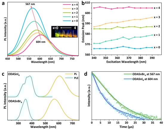
Figure 1.
(a) PL spectra of ODASnBr4−xIx; the inset is the photograph of ODASnBr4-xIx under 395 nm UV light. (b) PL peaks of ODASnBr4−xIx under different excitations. (c) PL and PLE spectra of ODASnI4 and ODASnBr4 microcrystals. (d) TRPL decay curves of ODASnI4 and ODASnBr4.
In addition, to verify that the synthesized perovskite is alloyed ODASnBr4-xIx rather than a simple mixture of ODASnBr4 and ODASnI4, the PL spectra of ODASnBr4-xIx under different excitations were further tested (Figure 1b and Figure S1). It can be seen from the variable excitation PL spectra that the emission peak wavelengths of ODASnBr4, ODASnBr2I2, and ODASnI4 are almost fixed, while those of ODASnBr1I3 and ODASnBr3I1 exhibit a redshift of up to about 10 nm with the change in the excitation from 340 nm to 390 nm. The excitation-independent PL emission exhibited by ODASnBr2I2 demonstrates that the alloying of Br− and I− forms a more homogeneous band structure. ODASnBr1I3 and ODASnBr3I1 exhibit a slight excitation-dependent phenomenon, implying that there is a localized aggregation of Br− and I− in the lattice, which results in different PL contributions under different excitations. Considering the good symmetry of the PL spectra of ODASnBr4−xIx and no occurrence of obvious dual emission phenomenon, it can be confirmed that the synthesized perovskites are halogen-alloyed ODASnBr4−xIx with different bromine/iodine ratios instead of a simple mixture of ODASnBr4 and ODASnI4 microcrystals.
It can be observed from the PL spectra that there is a significant difference between the PL peaks of ODASnI4 and ODASnBr4 (Figure 1c), which may be caused by the decrease in the radius of halogen ions, the contraction of the inorganic layer, and the increase in the bandgap during the substitution of the halogen from iodine to bromine [24,25]. ODASnBr4 and ODASnI4 microcrystals are both large in size and cannot be well dispersed in solution for absorption characterization. As a result, their UV–visible diffuse reflectance spectra were collected and converted into absorption spectra (Figure S2) by using the Kubelka–Munk (K-M) formula, which is shown in Equation (1).
where K is the absorption coefficient, S is the reflection coefficient, and R is the relative reflectivity of the approximately infinitely thick sample.
F(R) = K/S = (1 − R)2/(2R)
The absorption spectra can be used for obtaining the approximate bandgaps of the two mentioned perovskites by Tauc plot, which is shown in Equation (2).
where α is the absorption coefficient; h is Planck’s constant (h ≈ 4.13567 × 10⁻¹⁵ eV s); ν is the incident photon frequency (in ν = c/λ, c is the speed of light, c ≈ 3 × 10⁸ m/s, and λ is the wavelength of the incident light); n is a constant associated with the type of semiconductor material (n is 0.5 for materials of direct bandgap and 2 for that of indirect bandgap); B is a constant of proportionality; and Eg is the bandgap of the characterized semiconductor material.
(αhν)^(1/n) = B(hν − Eg)
When the absorption spectrum is converted by the Tauc plot, the section near the beginning can be fitted as a straight line, and its transverse intercept with the x-axis is the bandgap of the target material. The bandgaps of ODASnBr4 and ODASnI4 are 2.91 eV and 2.79 eV, respectively (Figure S3), which is in accordance with Vegard’s law [30]. However, the observed variation trend in bandgap remains consistent with experimental observations, which explains the blueshift of PL peaks from ODASnI4 to ODASnBr4.
The PL QY of ODASnI4 microcrystals reached 17% (Figure S4). As a comparison, ODASnBr4 microcrystals have a near-unity PL QY (99%), which exceeds the vast majority of 2D THPs mentioned in the Section 1 (Figure S5). It is worth noting that the PL QYs of perovskite samples are given by the integrating sphere method, as is widely recognized for the calculation of PL QY [31,32]. The remarkable difference in PL QY of ODASnI4 and ODASnBr4 is mainly caused by light-driven ligand-to-metal charge transfer (LD-LMCT), which manifests as the mutual oxidation of Sn2+ and I− in tin–iodide perovskites, exacerbating the oxidation issue and negatively affecting the luminescent performance of ODASnI4 [33]. Under ambient conditions, the oxidized Sn4+ undergoes electron exchange with I−, resulting in the reduction from Sn4+ to Sn2+ and oxidation from I− to I2. Nevertheless, the mentioned redox reaction proceeds in the reverse direction under light irradiation. Part of the Sn2+ cations re-oxidize to Sn4+, which subsequently reacts with I−, atmospheric water, and oxygen to form HI and SnO2. The generated HI further undergoes oxidation to produce I2 again. Such chain-like oxidation processes lead to rapid degradation of the pristine lattice through the formation of vacancy defects, thereby significantly compromising the luminescent properties of the tin–iodide perovskites.
The TRPL decay curves of ODASnI4 and ODASnBr4 are shown in Figure 1d, with the fitted lifetimes listed in Table 2. In the case of STE emission, the short exciton lifetime τ1 usually originates from the donor–acceptor pair recombination after the capture of carriers by surface defects, while the long exciton lifetime τ2 is based on the emission of STEs [34]. It is obvious that the proportion of surface defect capture in ODASnI4 is higher than that in ODASnBr4, and τ1 of ODASnI4 is also smaller than that of ODASnBr4, according to the calculated exciton lifetime. It is indicated that the oxidation phenomenon of ODASnI4 is more severe, with more tin vacancies on the surface, which enhances the non-radiative composites.
Table 2.
TRPL parameters of ODASnI4 and ODASnBr4 under optimal excitation.
To further verify the existence of LD-LMCT, high-resolution (HR) XPS spectra of ODASnI4 and ODASnBr4 for specific elements were characterized, in which the cyan solid lines represent the fitted spectra, and the black dashed lines represent the actual measured spectra. Fitting parameters of XPS spectra have been listed in Table S1.
The overall binding energy of N 1s in ODASnI4 is slightly higher than that in ODASnBr4, which may be caused by the alternation in coordination environments resulting from the use of different halogen ions I− and Br− (Figure 2a) [35]. The high-energy peak of the N 1s located near 401 eV and the low-energy peak near 400 eV correspond to -NH2+ and -NH3, respectively, suggesting a small amount of detached ODA [36]. This may originate from the excess precursor or the formation of halogen ion vacancies from the oxidation of I− and hydrogen bonding breakage leading to ODA2+ detachment.
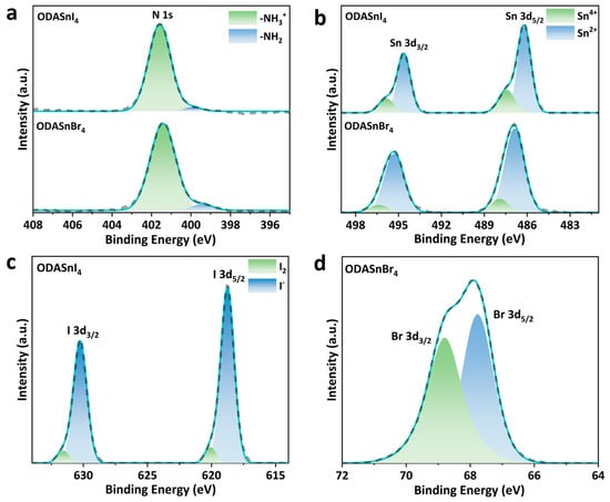
Figure 2.
HR XPS spectra of (a) N 1s and (b) Sn 3d in ODASnI4 and ODASnBr4. HR XPS spectra of (c) I 3d in ODASnI4 and (d) Br 3d in ODASnBr4.
The HR XPS spectra of Sn 3d in ODASnI4 and ODASnBr4 exhibit two asymmetric peaks corresponding to two spin-orbit splitting sub-energy levels, Sn 3d3/2 and Sn 3d5/2 (Figure 2b). The two low-energy peaks of Sn 3d in ODASnI4 located at 486.19 eV and 494.63 eV correspond to Sn2+, while the high-energy peaks at 487.42 eV and 495.87 eV imply the existence of Sn4+ [37]. As a comparison, the XPS spectrum of ODASnBr4 indicates a similar coexistence of Sn2+ and Sn4+, but the proportion of Sn4+ is lower than that in the XPS spectrum of ODASnI4, which substantiates that LD-LMCT results in a more pronounced oxidation problem in tin–iodide perovskites compared to their bromide counterparts. As mentioned before, oxidation of Sn2+ results in the formation of tin vacancies, which will become the non-radiative combination centers and degrade the PL QY of THPs.
The I 3d HR XPS spectrum of ODASnI4 exhibits very distinct multiple peaks in both I 3d3/2 and I 3d5/2 energy levels (Figure 2c). The low-energy peaks at 618.76 eV and 630.25 eV represent I− in the perovskite layer, whereas the peaks at 620.06 eV and 631.57 eV imply the transition from I− to I2 in ODASnI4, which further corroborates the oxidation caused by LD-LMCT. The Br 3d HR XPS spectrum of ODASnBr4 shows two overlapping binding energy peaks located at 67.77 eV and 68.80 eV, corresponding to Br 3d3/2 and Br 3d5/2, respectively (Figure 2d). The splitting energy of 1.03 eV is very close to the theoretical value of 1 eV, indicating the absence of Br− oxidation [38,39]. Percentages of the major elements calculated based on XPS spectra have been listed in Table S2.
It is worth mentioning that the oxidation of the internal part of ODASnI4 and ODASnBr4 microcrystals is much lower than that of the surface, according to previous reports [40], because the organic A-site cations are capable of preventing the penetration of water and oxygen. Compared to RP-phase 2D THPs (e.g., PEA2SnI4), DJ-phase 2D THPs have fewer oxidation-induced defects, which can suppress non-radiative recombination and result in higher PL QY [23].
Morphology characterizations on ODASnI4 and ODASnBr4 were also employed to further explore the reasons for the differences in the optical properties of these two perovskites. The interlayer spacings of ODASnI4 and ODASnBr4 calculated from XRD patterns are 1.37 nm and 1.39 nm, respectively (Figure S6). SEM images show that ODASnI4 and ODASnBr4 are both microcrystals with layered structures, which is a typical feature of 2D THPs. However, ODASnI4 microcrystals agglomerate into spheres (Figure 3a,b). On the contrary, the layered structure is distinct in ODASnBr4 samples (Figure 3c,d). The weak coordination ability of I− ions reduces the passivation efficiency of the active sites on the surface of the inorganic layer, as well as causing the (SnI6)4− octahedra to form thermodynamically more stable spherical agglomerates by adsorbing to each other via van der Waals forces.
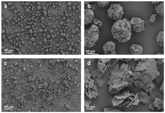
Figure 3.
SEM images of (a,b) ODASnI4 microcrystals and (c,d) ODASnBr4 microcrystals.
Figures S7 and S8 show the SEM images of ODASnI4 and ODASnBr4 microcrystals and the corresponding elemental mapping images. The uniform distribution of Sn, I, and N elements confirms the generation of pure ODASnBr4 and ODASnI4 microcrystals, but the distribution of N elements at the edges of the ODASnI4 spheres is less. This suggests that there may be ODA detached at the edge of the inorganic layer, which prompts the (SnI6)4− octahedra to agglomerate into spheres after mutual adsorption by van der Waals forces or halogen bonds. According to previous reports, the agglomeration of 2D perovskites can cause electronic defects and decreased quality of the perovskite crystals, as well as destroy the perpendicular quantum well orientation [41,42,43]. Furthermore, the agglomeration can also cause the optical phonon and defect scattering by reducing the screening of Coulomb potential, which leads to stronger non-radiative recombination [44].
FTIR spectra were employed to reveal the interaction of chemical bonds within ODASnI4 and ODASnBr4. There are no prominent broadband peaks from 3200 cm−1 to 3600 cm−1, which indicates the absence of significant O-H vibrations, proving that the solvent used in the reaction process is almost completely removed after purification (Figure S9). According to previous reports, the N-H stretching vibration based on the -NH2 group in free ODA molecules should be located at 3330 cm−1, whereas the N-H vibrations of both ODASnBr4 and ODASnI4 synthesized in this chapter are located at about 3090 cm−1, and the shift of vibrational frequency toward lower wavenumbers is attributed to the formation of hydrogen bonds between protonated ODA2+ cations and the inorganic layers [22,45]. Multiple peaks were observed in the range of 2800 cm−1 to 3000 cm−1 in ODASnBr4, and the peaks located at 2962 cm−1, 2928 cm−1 and 2854 cm−1 correspond to the C-H vibration of -CH3 in ODA, C-H symmetry vibration, and asymmetry vibration in -CH2-, respectively, which proves the integrity of ODA2+ carbon chains. Three sharper peaks can be observed in the range of 1300 cm−1 to 1700 cm−1, which corresponds to the bending vibration of -CH3 and correlates with the conformational ordering of the ODA, suggesting a certain degree of van der Waals’ force interaction within the organic layers, which is also in line with previous analysis in N 1s XPS spectra. According to the above analysis of N-H vibration and C-H vibration, it can be judged that ODA2+ cations are successfully embedded in the inorganic layer and connected to the inorganic layer via hydrogen bonding. In addition, it can be observed that the N-H peak of the ODASnI4 sample is more inclined to lower wavelengths compared to that of the ODASnBr4 sample, which is due to the stronger polarization ability of I− and the formation of stronger hydrogen bonding with the organic layer. The shift of the C-H vibration can be attributed to the effect of the larger ionic radius of I− on the organic layer.
ODASnBr4 has extremely remarkable luminescent performance, as described previously. The synthesized ODASnBr4 exhibits a broadband emission with the optimal excitation located at 354 nm, emission peak at 567 nm, and an FWHM of 114 nm. These luminescent properties make ODASnBr4 a promising candidate for WLED applications. Considering the need for commercialization, we optimized the synthesis conditions to maximize the yield while maintaining high PL QY. It should be noted that the yield of the synthesized ODASnI4 microcrystals was about 55% (0.4238 g), which may be caused by oxidation. Due to the LD-LMCT mechanism, tin–iodine perovskites are highly susceptible to oxidation and production of I2, which is soluble in ethyl acetate and is removed during purification, resulting in the yield reduction in the perovskite.
We investigated the effects of HI dosage, H3PO2 dosage, the type of tin precursors, and reaction temperature on the PL intensity and yield of ODASnBr4, respectively. The ODASnBr4 synthesized at different H3PO2 dosages exhibited different PL intensities, but their emission peaks remained near 567 nm (Figure S10). According to previous reports, the FWHM of STE emission in THPs depends on the length of the Sn-X bond, which is closely related to the synthesis environment [11]. The FWHM of ODASnBr4 remained constant, indicating that the aqueous-phase method applied in this article has excellent reproducibility. The highest PL intensity of ODASnBr4 was achieved at an H3PO2 dosage of 13.5 mL. Further increase in H3PO2 dosage leads to no further improvement in PL intensity, which indicates that the oxidation of Sn2+ has been completely inhibited. In addition, a rapid decrease in the yield of ODASnBr4 was observed under higher H3PO2 dosage. It is attributed to the fact that ODASnBr4 is very soluble in water, and the water introduced by additional H3PO2 could not be completely removed in the reaction, thus reducing the yield of perovskites.
In the aqueous-phase method for the synthesis of 2D THPs, an excess of hydrohalic acid is necessary to provide enough halogen ions for reducing halogen vacancies. No significant precipitation of perovskite was observed under the usage of 2 mL HI. When the amount of hydrobromic acid exceeded 3 mL, ODASnBr4 began to crystallize and precipitate, exhibiting the highest PL intensity at 4 mL and a gradual decrease thereafter. (Figure S11) The effect of excessive halogen ions on reducing vacancy defects has been widely recognized, which explains the increase in PL intensity as the amount of HBr rises from 2 mL to 4 mL [46,47]. Nevertheless, additional HBr introduced excessive oxygen and water into the solvent, which may induce the oxidation of Sn2+. Too many halogen ions may also cause deep traps and halide-rich defects, leading to the enhancement of nonradiative recombination and a decrease in optical properties with higher HBr dosages [48,49].
Different bivalent tin compounds were used as precursors. ODASnBr4 was synthesized using stannous oxalate (SnOAc2), stannous bromide (SnBr2), and stannous oxide (SnO). The highest PL intensity was achieved with SnO (Figure S12). Furthermore, heating is required for the synthesis of ODASnBr4 in the aqueous-phase method for dissolution of the precursors and precipitation of the perovskite by evaporating the solvent. ODASnBr4 was synthesized at different temperatures within 30 min. No precipitation of ODASnBr4 was observed at 80 °C, so the reaction time was extended to 60 min. Considering that too long a reaction time may lead to oxidation of Sn2+, no further attempts were made at synthesis temperatures below 80 °C. The PL intensity showed a positive correlation with the reaction temperature, reaching a maximum at 95 °C (Figure S13). At 100 °C, an abnormal decrease was observed in both PL intensity and yield. It may be caused by the co-evaporation of H3PO2, which has a low boiling point of 108 °C, with water, leading to the oxidation of Sn2+ during the reaction.
The yields of ODASnBr4 under different experimental conditions are calculated and listed in Tables S3. By optimizing the experimental conditions, it was possible to achieve a yield of approximately 90%. The experimental conditions of 4 mL HBr, 13.5 mL H3PO2, 1 mmol SnO, and 1.2 mmol ODA co-heated at 90 °C for 30 min were finally chosen for this article, as both the PL intensity and the yield were satisfactory under this condition. Meanwhile, due to the excellent reproducibility and simplicity of the process of the aqueous-phase method, a gram-scale production of ODASnBr4 microcrystals (1.3441 g) can be achieved by simply tripling the amount of precursor (Figure S14), and the yield under such conditions is 80.18%, which is a highly efficient and large-volume preparation method that is relatively rare in reports of 2D THPs.
ODASnBr4 has the advantage of broadband emission with high PL QY, which makes it a promising luminescent material for WLED applications. Therefore, stability tests were conducted to ensure that this kind of STE-emitting 2D THP can be used as a long-lasting phosphor after encapsulation. Based on the application scenarios of WLEDs, the thermal stability, photostability, and air stability of ODASnBr4 were tested, respectively.
In the thermal stability test, the ground ODASnBr4 microcrystals were sealed in flat-bottomed glass vials and heated for 4 h at 90 °C, which was selected because it approximates the operating conditions of a 3W LED chip. To ensure that the ODASnBr4 samples are not affected by other environmental conditions (e.g., oxidation due to exposure to air), the samples for characterization were weighed from continuously heated and unopened glass vials. The result exhibited that the PL intensity of ODASnBr4 decreased approximately linearly with time and remained at about 90% of the original PL intensity after 4 h of heating (Figure S15). In addition, the thermal stability test was also operated at 70 °C and 120 °C to simulate moderate and extreme conditions under the operation of LED. It is observed that the ODASnBr4 microcrystals exhibited a similar linear downward trend in PL intensity under both temperatures, which further verified their good thermal stability.
In the photostability test, a 16 W UV light was used for photo-aging. The PL intensity of ODASnBr4 exhibited a significant decrease in the first hour but gradually stabilized in the subsequent tests and remained 68.2% of the original intensity after being continuously irradiated for 72 h (Figure S16).
In addition, ODASnBr4 powder was placed in a room-temperature ambient environment for 72 h. The PL intensity of ODASnBr4 decreased slowly and linearly with time and retained 89.90% of the initial PL intensity after 72 h (Figure S17). It is worth noting that the wavelength changes in the emission peaks remained within 3 nm during previous stability tests, indicating remarkable color stability of ODASnBr4 (Figure S18).
The synthesized ODASnBr4 microcrystals with broadband yellow emission were mixed with commercially available BaMg2Al16O27:Eu2+ (BMA) blue phosphor, then encapsulated on a 365 nm UV chip, with a view to obtaining a two-component WLED with excellent LE and Ra. A series of WLEDs with different EL spectra were prepared by varying the blending ratios of ODASnBr4 microcrystals and BMA phosphor. It can be observed that the EL intensity of both phosphors increases steadily with increasing current, and the increase in blending ratio of ODASnBr4/BMA from 1:1 to 3:1 can significantly enhance the EL intensity of ODASnBr4 (Figure 4a–c). Varying the blending ratio of ODASnBr4 and BMA can significantly move the color coordinates of the prepared WLEDs from (0.2406, 0.1928) (1:1) to (0.3023, 0.2761) (2:1) and (0.3321, 0.3167) (3:1) (Figure 4d).
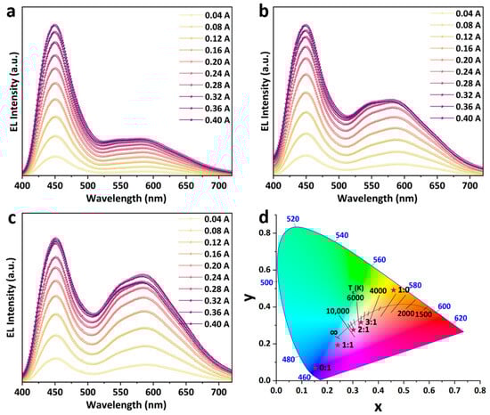
Figure 4.
EL spectra of WLEDs prepared with ODASnBr4 and BMA phosphors at blending ratios of (a) 1:1, (b) 2:1, and (c) 3:1 under different driving currents. (d) CIE chromaticity coordinates of ODASnBr4, BMA phosphor, and the WLEDs prepared with different blending ratios. Red stars correspond to CIE coordinates of WLEDs with different blending ratios (annotated adjacent to each red star).
The LE and Ra of the LEDs prepared with different ODASnBr4/BMA blending ratios also exhibited regular changes with the driving current. Notably, the LE of ODASnBr4 reached up to 121.05 lm/W when encapsulated on the UV chip alone (Figure 5a), and that of WLEDs with blending ratios of 1:1, 2:1, and 3:1 exhibited a measurable reduction, which might originate from the energy transfer between ODASnBr4 and BMA. The EL spectra of the prepared WLEDs were more homogeneous due to the blending of blue phosphor, thus leading to a distinct increase in Ra (Figure 5b–d). WLEDs with a blending ratio of 2:1 exhibited the best LE and Ra compared to the WLEDs with different blending ratios. The WLED with a blending ratio of 2:1 has a highest Ra of 91.9, and its LE reaches up to 96.27 lm/W under a driving current of 0.12 A (Table S4).
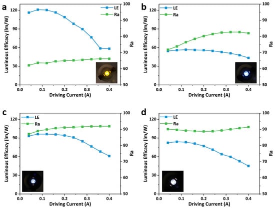
Figure 5.
Luminous efficacy and CRI of the prepared WLEDs with blending ratios of ODASnBr4 and BMA phosphors of (a) 1:0, (b) 1:1, (c) 2:1, and (d) 3:1 under different driving currents. The insets are photographs of the correlated LEDs under a current of 0.1 A.
The WLED with a blending ratio of 2:1 was placed under a driving current of 100 mA for 40 min, and the luminescent data were recorded every minute. After 40 min, the EL intensities of both BMA and ODASnBr4 slightly decreased. LE of the WLED showed a nearly linear decrease and remained 93.24% of the original LE after 40 min (Figure S19). The CIE coordinates of the WLED showed only a slight drift from the original (0.3043, 0.2680) to (0.3040, 0.2737) (Figure S20). The above results indicate that the WLEDs prepared via ODASnBr4 have excellent luminescent performance and stability, while further studies remain necessary to meet the demand of commercialization.
4. Conclusions
In summary, ODASnI4 and ODASnBr4 microcrystals were synthesized by a facile aqueous-phase method. The effect of LD-LMCT on these two perovskites is exposed by discussing their difference in optical properties as well as morphology, which is mainly caused by the co-oxidation of Sn2+ and I−. The optimization of synthesis conditions obtained ODASnBr4 microcrystals with high yield (approximately 90%), broadband yellow emission, near-unity PL QY, and remarkable stability. After that, the WLEDs prepared with ODASnBr4 microcrystals and BMA phosphors exhibited an Ra of 91.9 and a maximum LE of over 96 lm/W. This article systematically discussed the optical properties of ODASnX4 (X = Br, I), highlighting their potential in high-performance, environmentally friendly solid-state lighting applications.
Supplementary Materials
The following supporting information can be downloaded at: https://www.mdpi.com/article/10.3390/nano15110818/s1. Figure S1. PL spectra of ODASnBr4-xIx microcrystals under different excitations when (a) x = 4, (b) x = 3, (c) x = 2, (d) x = 1, and (e) x = 0. Figure S2. Diffuse reflectance spectra of (a) ODASnI4 and (b) ODASnBr4 represented by the K-M function. Figure S3. Tauc plot of (a) ODASnI4 and (b) ODASnBr4. Figure S4. PL spectra of ODASnI4 for the calculation of PL QY. Figure S5. PL spectra of ODASnBr4 for the calculation of PL QY. Figure S6. XRD patterns of ODASnI4 and ODASnBr4. Figure S7. (a) SEM image and element mapping images of (b) Sn, (c) I, and (d) N atoms of ODASnI4 microcrystals. Figure S8. (a) SEM image and element mapping images of (b) Sn, (c) Br, and (d) N atoms of ODASnBr4 microcrystals. Figure S9. (a) FTIR spectrum and (b), (c) enlarged spectrum of ODASnX4 (X = Br, I). Figure S10. PL spectra of ODASnBr4 synthesized with different amounts of H3PO2. Figure S11. PL spectra of ODASnBr4 synthesized with different amounts of HBr. Figure S12. PL spectra of ODASnBr4 synthesized with different tin precursors. Figure S13. PL spectra of ODASnBr4 synthesized with different reaction temperatures. Figure S14. Photographs of ODASnBr4 microcrystals prepared in large quantities in different states. From left to right are photographs of (a) precursor, (b) solution after heating, (c) perovskite after crystallization, and (d) perovskite microcrystals under 365 nm UV light. Figure S15. PL spectra of ODASnBr4 as a function of time in thermal stability test under (a) 70 °C, (b) 90 °C, and (c) 120 °C. Figure S16. PL spectra of ODASnBr4 as a function of time in the photostability test. Figure S17. PL spectra of ODASnBr4 as a function of time in the air stability test. Figure S18. Relative intensity and PL peaks of ODASnBr4 as a function of time in (a) thermal (90 °C), (b) photo, and (c) air stability tests. Figure S19. (a) EL spectra and (b) LE of the prepared WLED with a blending ratio of 2:1 before and after the stability test. Figure S20. CIE chromaticity coordinates of the WLED (a) before and (b) after stability test. Table S1. Fitting parameters in XPS spectra. Table S2. Percentages of the major elements calculated based on XPS spectra. Table S3. Yield of ODASnBr4 calculated by tin under different experimental conditions; “/” represents no production. Table S4. Performance parameters of WLED prepared with ODASnBr4 and BMA under a 2:1 blending ratio.
Author Contributions
Conceptualization, Y.X. and H.H.; methodology, Y.X. and H.H.; software, J.Y. and D.Z.; validation, Y.X., J.Y., H.H., and J.Z.; formal analysis, Y.X. and J.Z.; investigation, J.Y. and Y.Q.; resources, Y.X. and S.M.; data curation, Y.X.; writing—original draft preparation, Y.X.; writing—review and editing, Y.X., J.Y., and Y.Q.; visualization, Y.X.; supervision, S.M., W.Z., and R.G.; project administration, S.M. and R.G.; funding acquisition, S.M. and R.G. All authors have read and agreed to the published version of the manuscript.
Funding
This work was supported by the National Key Research and Development Program of China (2024YFE0204600), the National Natural Science Foundation of China (No. 62074044), the Natural Science Foundation of Shanghai (24ZR1405600), the Open Research Project Programme funded by the Science and Technology Development Fund (006/2022/ALC), and the Macao Centre for Research and Development in Advanced Materials (University of Macau) (Ref. No.: MCRDAM-IAPME(UM)-2022-2024/ORP/003/2023).
Data Availability Statement
Data are contained within this article.
Conflicts of Interest
The authors declare no conflicts of interest.
References
- Sun, S.Q.; Tai, J.W.; He, W.; Yu, Y.J.; Feng, Z.Q.; Sun, Q.; Tong, K.N.; Shi, K.; Liu, B.C.; Zhu, M.; et al. Enhancing Light Outcoupling Efficiency via Anisotropic Low Refractive Index Electron Transporting Materials for Efficient Perovskite Light-Emitting Diodes. Adv. Mater. 2024, 36, 2400421. [Google Scholar] [CrossRef] [PubMed]
- Feng, S.C.; Shen, Y.; Hu, X.M.; Su, Z.H.; Zhang, K.; Wang, B.F.; Cao, L.X.; Xie, F.M.; Li, H.Z.; Gao, X.; et al. Efficient and Stable Red Perovskite Light-Emitting Diodes via Thermodynamic Crystallization Control. Adv. Mater. 2024, 36, 2410255. [Google Scholar] [CrossRef] [PubMed]
- Sun, S.-Q.; Sun, Q.; Cai, Y.; Feng, Z.-Q.; Zheng, Q.; Liu, B.; Zhu, M.; Shi, T.; Liao, L.-S.; Xie, Y.-M.; et al. Mitigation of Nonradiative Recombination by Reconfiguring Triplet Energy of Additive Toward Efficient Blue Perovskite Light-Emitting Diodes. ACS Nano 2025, 19, 13053–13062. [Google Scholar] [CrossRef]
- He, H.; Yin, J.; Zhao, D.; Xing, Y.; Wang, B.; Xing, G.; Tian, P.; Zhang, W.; Mei, S.; Guo, R. Ethylenediammonium-asisted phase control and in-situ passivation of all-bromine quasi-2D perovskite for efficient pure-blue light-emitting diodes. Chem. Eng. J. 2025, 508, 160440. [Google Scholar] [CrossRef]
- He, H.; Mei, S.; Wen, Z.; Yang, D.; Yang, B.; Zhang, W.; Xie, F.; Xing, G.; Guo, R. Recent Advances in Blue Perovskite Quantum Dots for Light-Emitting Diodes. Small 2022, 18, 2103527. [Google Scholar] [CrossRef]
- Mei, S.; Yin, J.; Xing, Y.; He, H.; Gu, H.; Xia, J.; Zhang, W.; Liang, C.; Xing, G.; Guo, R. Designing High-Performance Pure-Red Metal Halide Perovskite Materials and Light-Emitting Diodes for Rec. 2020 Display. Nano Energy 2024, 122, 109339. [Google Scholar] [CrossRef]
- Zhang, Y.; Park, N.-G. Quasi-Two-Dimensional Perovskite Solar Cells with Efficiency Exceeding 22%. ACS Energy Lett. 2022, 7, 757–765. [Google Scholar] [CrossRef]
- Xu, T.; Liu, S.; Il Seok, S.; Xiang, W. Surface chemistry-induced reconstruction of inorganic perovskites for efficient and stable inverted solar cells. Joule 2025, 9, 101826. [Google Scholar] [CrossRef]
- Liu, Z.; Zhang, Z.; Liu, Y.; Luo, R.; Cheng, Y.; Shen, Y.; Wang, K.; Wang, M. Boosting Carrier Mobility in 2D Layered Perovskites for High-Performance UV Photodetector. Small Methods 2025, 9, 2400887. [Google Scholar] [CrossRef]
- Jiao, Z.; Wang, X.; Gao, J.; Huang, X.; Wang, Y. Waterproof Perovskite Quantum Dots for In-vivo Photoluminescence Bioimaging. Chem. Res. Chin. Univ. 2024, 40, 901–906. [Google Scholar] [CrossRef]
- Gualdrón-Reyes, A.F. Self-Trapped Exciton versus Band-Edge Electron Transitions: Insights of the Factors Affecting the Optical Properties of Lead-Free Sn-Halide Perovskites. Adv. Opt. Mater. 2025, 13, 2402043. [Google Scholar] [CrossRef]
- Xing, Y.; He, H.; Cui, Z.; Fu, Z.; Qin, S.; Zhang, W.; Mei, S.; Guo, R. Recent Advances in Optical Properties and Light-Emitting Diode Applications for 2D Tin Halide Perovskites. Adv. Opt. Mater. 2024, 12, 2302679. [Google Scholar] [CrossRef]
- Wang, A.; Guo, Y.; Zhou, Z.; Niu, X.; Wang, Y.; Muhammad, F.; Li, H.; Zhang, T.; Wang, J.; Nie, S.; et al. Aqueous Acid-Based Synthesis of Lead-Free Tin Halide Perovskites with Near-Unity Photoluminescence Quantum Efficiency. Chem. Sci. 2019, 10, 4573–4579. [Google Scholar] [CrossRef] [PubMed]
- Li, Z.L.; Deng, Z.T.; Johnston, A.; Luo, J.W.; Chen, H.J.; Dong, Y.T.; Sabatini, R.; Sargent, E.H. Precursor Tailoring Enables Alkylammonium Tin Halide Perovskite Phosphors for Solid-State Lighting. Adv. Funct. Mater. 2022, 32, 2111346. [Google Scholar] [CrossRef]
- Chen, Y.; Wang, Z.; Wei, Y.; Liu, Y.; Hong, M. Exciton Localization for Highly Luminescent Two-Dimensional Tin-Based Hybrid Perovskites through Tin Vacancy Tuning. Angew. Chem. Int. Ed. 2023, 62, 202301684. [Google Scholar] [CrossRef]
- Zhang, X.; Wang, C.; Zhang, Y.; Zhang, X.; Wang, S.; Lu, M.; Cui, H.; Kershaw, S.V.; Yu, W.W.; Rogach, A.L. Bright Orange Electroluminescence from Lead-Free Two-Dimensional Perovskites. ACS Energy Lett. 2018, 4, 242–248. [Google Scholar] [CrossRef]
- Hou, L.; Zhu, Y.H.; Zhu, J.R.; Li, C.Z. Tuning Optical Properties of Lead-Free 2D Tin-Based Perovskites with Carbon Chain Spacers. J. Phys. Chem. C 2019, 123, 31279–31285. [Google Scholar] [CrossRef]
- Liu, Y.; Wang, A.F.; Wu, J.J.; Wang, C.Y.; Li, Z.L.; Hu, G.C.; Sui, S.Q.; She, J.X.; Meng, W.; Li, W.Q.; et al. Alkylamine Screening and Zinc Doping of Highly Luminescent 2D Tin-Halide Perovskites for LED Lighting. Mater. Adv. 2021, 2, 1320–1327. [Google Scholar] [CrossRef]
- Wang, S.X.; Popovic, J.; Burazer, S.; Portniagin, A.; Liu, F.Z.; Low, K.H.; Duan, Z.H.; Li, Y.X.; Xiong, Y.; Zhu, Y.M.; et al. Strongly Luminescent Dion-Jacobson Tin Bromide Perovskite Microcrystals Induced by Molecular Proton Donors Chloroform and Dichloromethane. Adv. Funct. Mater. 2021, 31, 2102182. [Google Scholar] [CrossRef]
- Qi, J.; Wang, S.; Portniagin, A.; Kershaw, S.V.; Rogach, A.L. Room Temperature Fabrication of Stable, Strongly Luminescent Dion-Jacobson Tin Bromide Perovskite Microcrystals Achieved through Use of Primary Alcohols. Nanomaterials 2021, 11, 2738. [Google Scholar] [CrossRef]
- Wang, S.X.; Kershaw, T.H.; Rogach, A.R. Bright and Stable Dion-Jacobson Tin Bromide Perovskite Microcrystals Realized by Primary Alcohol Dopants. Chem. Mater. 2021, 33, 5413–5421. [Google Scholar] [CrossRef]
- Zhang, L.; Yang, B.B.; Mei, S.L.; Zhu, Y.X.; Hu, R.R.; Zou, J. Highly Luminescent Broadband Phosphors Based on Acid Solvent Coordinated Two-Dimensional Layered Tin-Based Perovskites. J. Mater. Chem. C 2022, 10, 3856–3862. [Google Scholar] [CrossRef]
- Mandal, A.; Roy, S.; Mondal, A.; Gupta, S.; Pal, B.; Bhattacharyya, S. Spacer Switched Two-Dimensional Tin Bromide Perovskites Leading to Ambient-Stable Near-Unity Photoluminescence Quantum Yield. J. Phys. Chem. Lett. 2022, 13, 9103–9113. [Google Scholar] [CrossRef] [PubMed]
- Chen, M.Y.; Lin, J.T.; Hsu, C.S.; Chang, C.K.; Chiu, C.W.; Chen, H.M.; Chou, P.T. Strongly Coupled Tin-Halide Perovskites to Modulate Light Emission: Tunable 550-640 nm Light Emission (FWHM 36-80 nm) with a Quantum Yield of up to 6.4%. Adv. Mater. 2018, 30, 1706592. [Google Scholar] [CrossRef]
- Yao, R.; Lin, J.; Liu, K.; Xu, Y.; Xiao, B.; Zhao, J.; Guo, Z.; Liu, Q.; Yuan, W. Structure and Optical Properties of Sn-Based Halide Perovskites (C10H18N2)SnX4 (X = Cl, Br, I). ACS Omega 2024, 9, 22352–22359. [Google Scholar] [CrossRef]
- Lanzetta, L.; Marin-Beloqui, J.M.; Sanchez-Molina, I.; Ding, D.; Haque, S.A. Two-Dimensional Organic Tin Halide Perovskites with Tunable Visible Emission and Their Use in Light-Emitting Devices. ACS Energy Lett. 2017, 2, 1662–1668. [Google Scholar] [CrossRef]
- Yuan, F.; Zheng, X.; Johnston, A.; Wang, Y.K.; Zhou, C.; Dong, Y.; Chen, B.; Chen, H.; Fan, J.Z.; Sharma, G.; et al. Color-Pure Red Light-Emitting Diodes Based on Two-Dimensional Lead-Free Perovskites. Sci. Adv. 2020, 6, eabb0253. [Google Scholar] [CrossRef]
- Liang, H.; Yuan, F.; Johnston, A.; Gao, C.; Choubisa, H.; Gao, Y.; Wang, Y.K.; Sagar, L.K.; Sun, B.; Li, P.; et al. High Color Purity Lead-Free Perovskite Light-Emitting Diodes via Sn Stabilization. Adv. Sci. 2020, 7, 1903213. [Google Scholar] [CrossRef]
- Roy, C.R.; Zhou, Y.; Kohler, D.D.; Zhu, Z.; Wright, J.C.; Jin, S. Intrinsic Halide Immiscibility in 2D Mixed-Halide Ruddlesden–Popper Perovskites. ACS Energy Lett. 2022, 7, 3423–3431. [Google Scholar] [CrossRef]
- Li, S.; Jiang, Y.; Xu, J.; Wang, D.; Ding, Z.; Zhu, T.; Chen, B.; Yang, Y.; Wei, M.; Guo, R.; et al. High-Efficiency and Thermally Stable FACsPbI3 Perovskite Photovoltaics. Nature 2024, 635, 82–88. [Google Scholar] [CrossRef]
- Wu, L.; Li, R.; Wen, W.; Zou, Q.; Ye, H.; Li, J. Lead-free hybrid indium perovskites with near-unity PLQY and white light emission using an Sb3+doping strategy. Inorg. Chem. Front. 2023, 10, 3297–3306. [Google Scholar] [CrossRef]
- Li, X.; Xia, M.; Li, W.; Lu, P.; Zhang, X.; Xu, Y. Lead-free Halide Perovskites With ≈100% PLQY and Dual-Color Emission for White Light-Emitting Diodes. Laser Photonics Rev. 2024, 19, 2401084. [Google Scholar] [CrossRef]
- Webb, T.; Haque, S.A. A Comparison of Molecular Iodine Evolution on the Chemistry of Lead and Tin Perovskites. Energy Environ. Sci. 2024, 17, 3244–3269. [Google Scholar] [CrossRef]
- Sun, S.; Lu, M.; Gao, X.; Shi, Z.; Bai, X.; Yu, W.W.; Zhang, Y. 0D Perovskites: Unique Properties, Synthesis, and Their Applications. Adv. Sci. 2021, 8, 2102689. [Google Scholar] [CrossRef]
- Min, H.; Lee, D.Y.; Kim, J.; Kim, G.; Lee, K.S.; Kim, J.; Paik, M.J.; Kim, Y.K.; Kim, K.S.; Kim, M.G.; et al. Perovskite Solar Cells with Atomically Coherent Interlayers on SnO2 Electrodes. Nature 2021, 598, 444–450. [Google Scholar] [CrossRef]
- Luangwanta, T.; Turren-Cruz, S.-H.; Masi, S.; Das Adhikari, S.; Recalde, I.B.; Zanatta, M.; Iglesias, D.; Rodríguez-Pereira, J.; Gené-Marimon, S.; Martinez-Ferrero, E.; et al. Enabling White Color Tunability in Complex 3D-printed Composites by Using Lead-Free Self-Trapped Exciton 2D Perovskite/Carbon Quantum Dot Inks. Nanoscale 2024, 16, 10262–10272. [Google Scholar] [CrossRef]
- Heo, Y.J.; Jang, H.J.; Lee, J.H.; Jo, S.B.; Kim, S.; Ho, D.H.; Kwon, S.J.; Kim, K.; Jeon, I.; Myoung, J.M.; et al. Enhancing Performance and Stability of Tin Halide Perovskite Light Emitting Diodes via Coordination Engineering of Lewis Acid-Base Adducts. Adv. Funct. Mater. 2021, 31, 2106974. [Google Scholar] [CrossRef]
- Li, X.; Wang, Y.; Lu, J.; Li, P.; Huang, Z.; Liang, G.; He, H.; Zhi, C. Constructing Static Two-Electron Lithium-Bromide Battery. Sci. Adv. 2024, 10, eadl0587. [Google Scholar] [CrossRef]
- Liu, Y.; Wang, J.; Wang, F.; Cheng, Z.; Fang, Y.; Chang, Q.; Zhu, J.; Wang, L.; Wang, J.; Huang, W.; et al. Full-Frame and High-Contrast Smart Windows from Halide-Exchanged Perovskites. Nat. Commun. 2021, 12, 3360. [Google Scholar] [CrossRef]
- Triggs, C.T.; Ross, R.D.; Mihalyi-Koch, W.; Clewett, C.F.M.; Sanders, K.M.; Guzei, I.A.; Jin, S. Spacer Cation Design Motifs for Enhanced Air Stability in Lead-Free 2D Tin Halide Perovskites. ACS Energy Lett. 2024, 9, 1835–1843. [Google Scholar] [CrossRef]
- Bonomi, S.; Armenise, V.; Accorsi, G.; Colella, S.; Rizzo, A.; Fracassi, F.; Malavasi, L.; Listorti, A. The Effect of Extended Ball-Milling upon Three-Dimensional and Two-Dimensional Perovskite Crystals Properties. Appl. Sci. 2020, 10, 4775. [Google Scholar] [CrossRef]
- Zhang, X.; Munir, R.; Xu, Z.; Liu, Y.; Tsai, H.; Nie, W.; Li, J.; Niu, T.; Smilgies, D.M.; Kanatzidis, M.G.; et al. Phase Transition Control for High Performance Ruddlesden–Popper Perovskite Solar Cells. Adv. Mater. 2018, 30, 1707166. [Google Scholar] [CrossRef]
- Xu, H.; Jiang, Y.; He, T.; Li, S.; Wang, H.; Chen, Y.; Yuan, M.; Chen, J. Orientation Regulation of Tin-Based Reduced-Dimensional Perovskites for Highly Efficient and Stable Photovoltaics. Adv. Funct. Mater. 2019, 29, 1807696. [Google Scholar] [CrossRef]
- Guo, Z.; Wu, X.; Zhu, T.; Zhu, X.; Huang, L. Electron–Phonon Scattering in Atomically Thin 2D Perovskites. ACS Nano 2016, 10, 9992–9998. [Google Scholar] [CrossRef]
- Yang, B.; Mei, S.; He, H.; Zhu, Y.; Hu, R.; Zou, J.; Xing, G.; Guo, R. Lead Oxide Enables Lead Volatilization Pollution Inhibition and Phase Purity Modulation in Perovskite Quantum Dots Embedded Borosilicate Glass. J. Eur. Ceram. Soc. 2022, 42, 258–265. [Google Scholar] [CrossRef]
- Qu, R.; Gao, M.; Li, H.; Qi, X.; Liu, C.; Zhao, W.; Yan, J.; Zhang, Z. Hydrobromic acid-assisted size control of formamidinium lead bromide perovskite quantum dots at room temperature. Opt. Mater. 2021, 113, 110776. [Google Scholar] [CrossRef]
- Ji, S.; Yuan, X.; Ji, W.; Li, H.; Zhao, J.; Zhang, H. Near-unity photoluminescence quantum yield Mn-doped two-dimensional halide perovskite platelets via hydrobromic acid-assisted synthesis. J. Lumin. 2022, 245, 118790. [Google Scholar] [CrossRef]
- Xu, J.; Buin, A.; Ip, A.H.; Li, W.; Voznyy, O.; Comin, R.; Yuan, M.; Jeon, S.; Ning, Z.; McDowell, J.J.; et al. Perovskite–fullerene hybrid materials suppress hysteresis in planar diodes. Nat. Commun. 2015, 6, 7081. [Google Scholar] [CrossRef]
- Chen, B.; Rudd, P.N.; Yang, S.; Yuan, Y.; Huang, J. Imperfections and their passivation in halide perovskite solar cells. Chem. Soc. Rev. 2019, 48, 3842–3867. [Google Scholar] [CrossRef]
Disclaimer/Publisher’s Note: The statements, opinions and data contained in all publications are solely those of the individual author(s) and contributor(s) and not of MDPI and/or the editor(s). MDPI and/or the editor(s) disclaim responsibility for any injury to people or property resulting from any ideas, methods, instructions or products referred to in the content. |
© 2025 by the authors. Licensee MDPI, Basel, Switzerland. This article is an open access article distributed under the terms and conditions of the Creative Commons Attribution (CC BY) license (https://creativecommons.org/licenses/by/4.0/).