


Integrating Fluorescent Nanodiamonds into Polymeric Microstructures Fabricated by Two-Photon Polymerization


 , , and
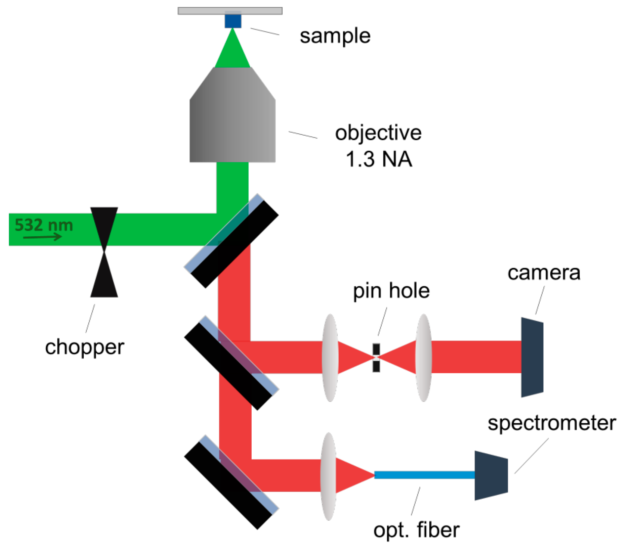
Abstract
:1. Introduction
2. Materials and Methods
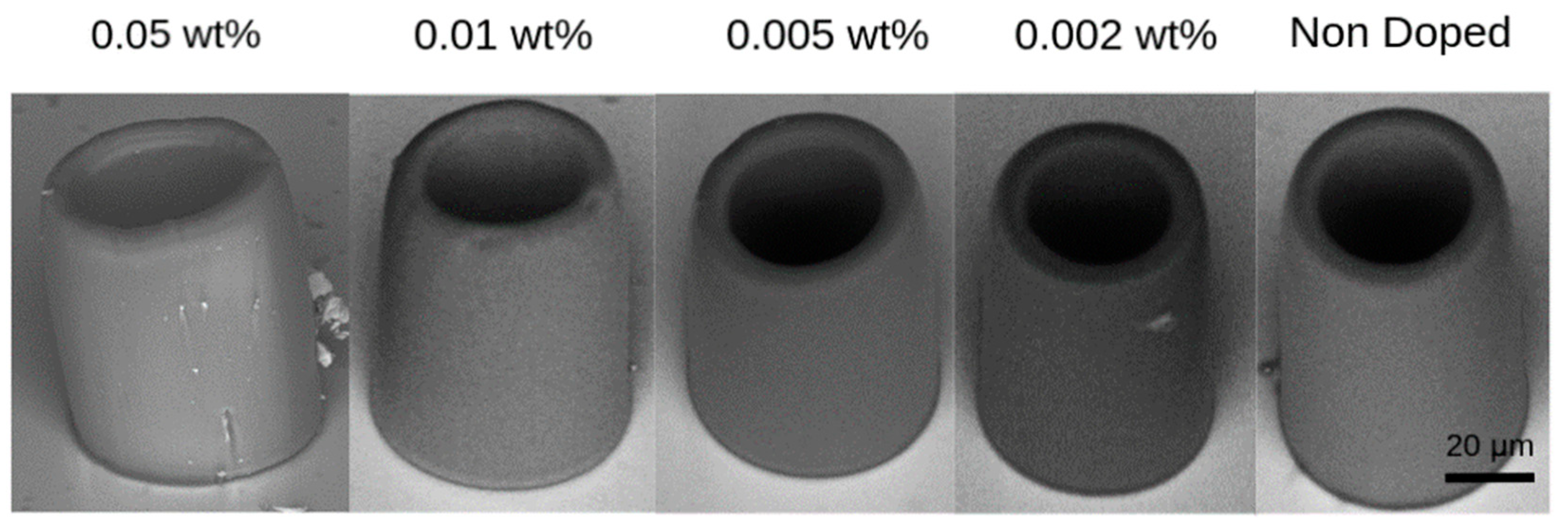
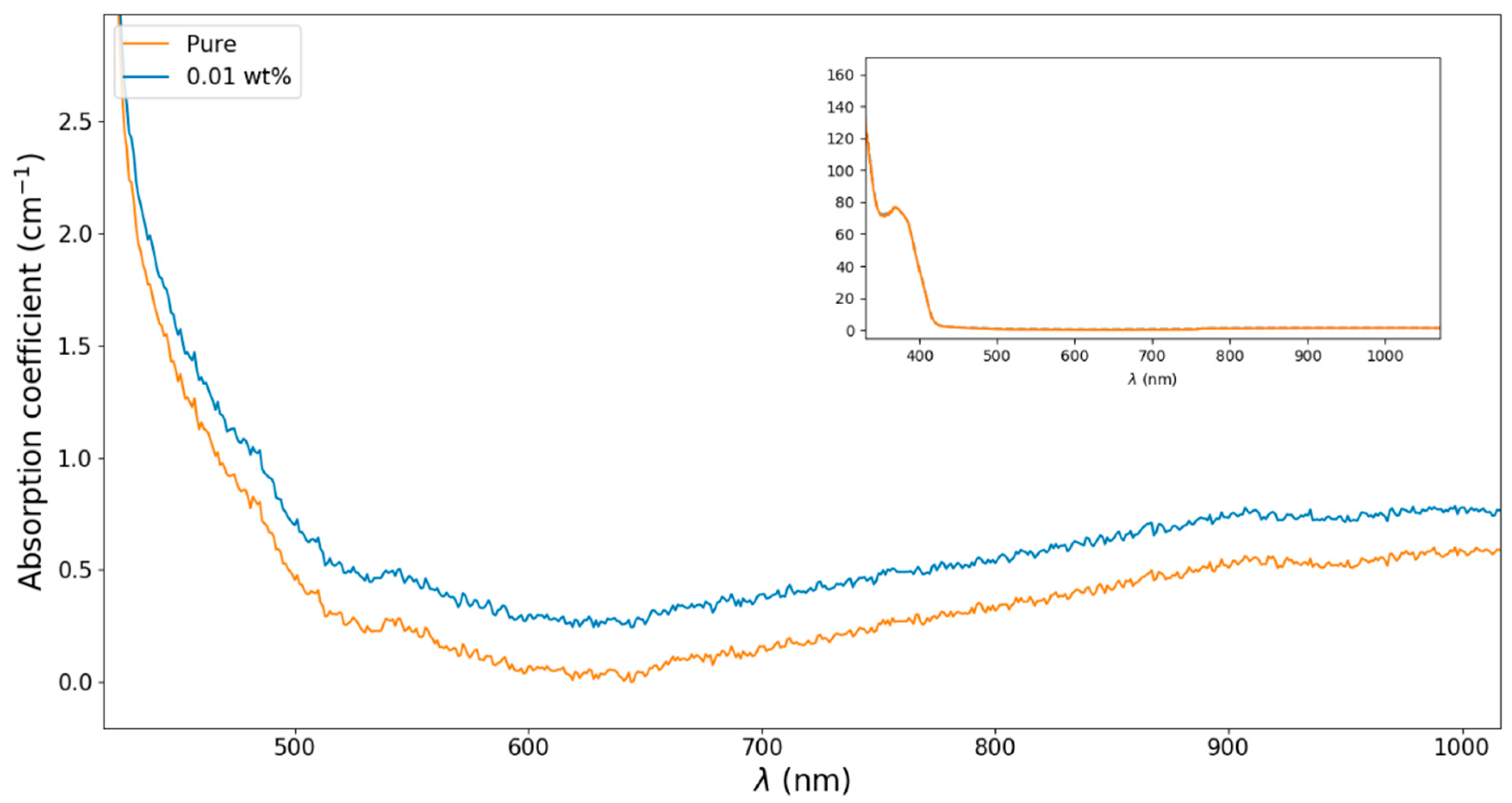
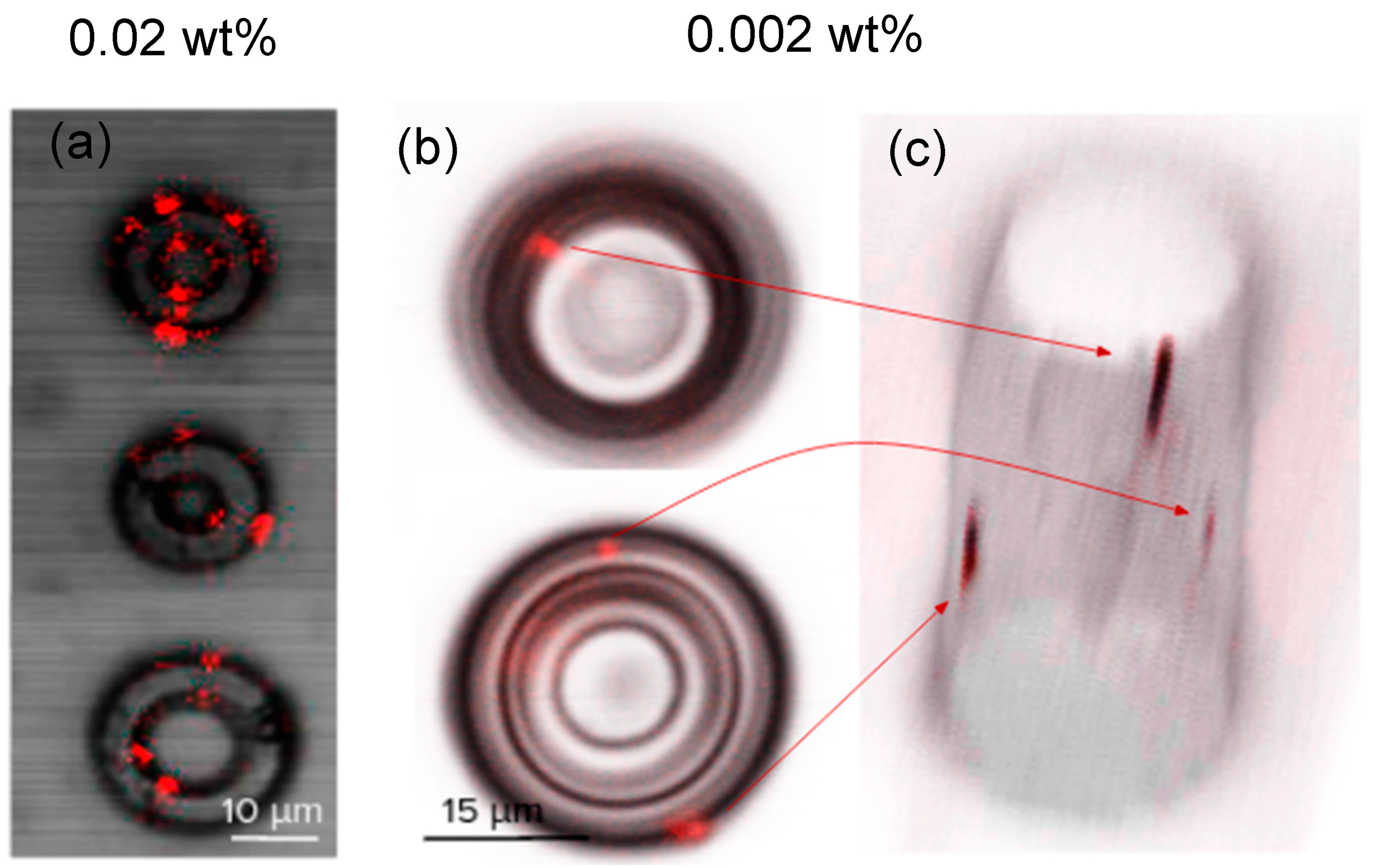
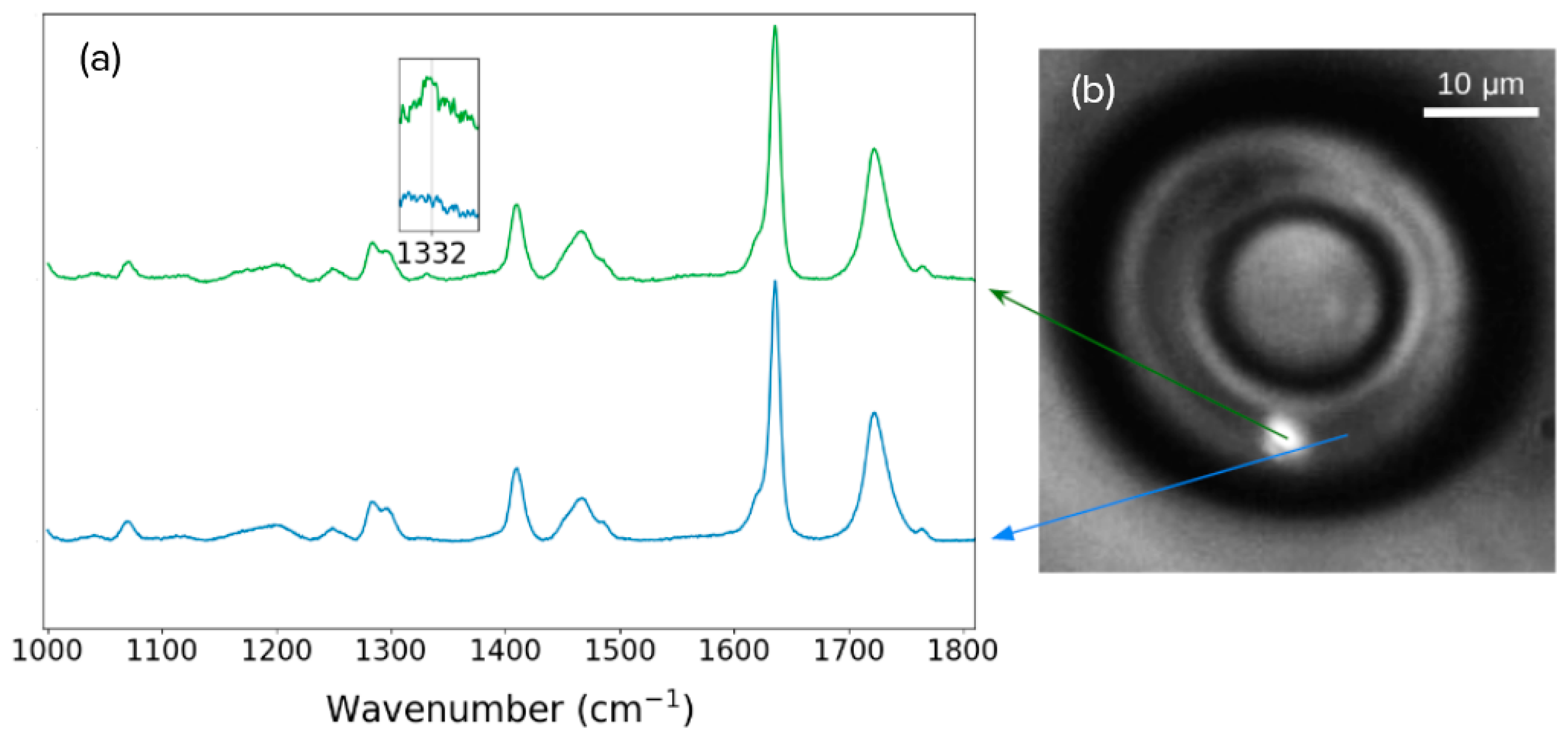
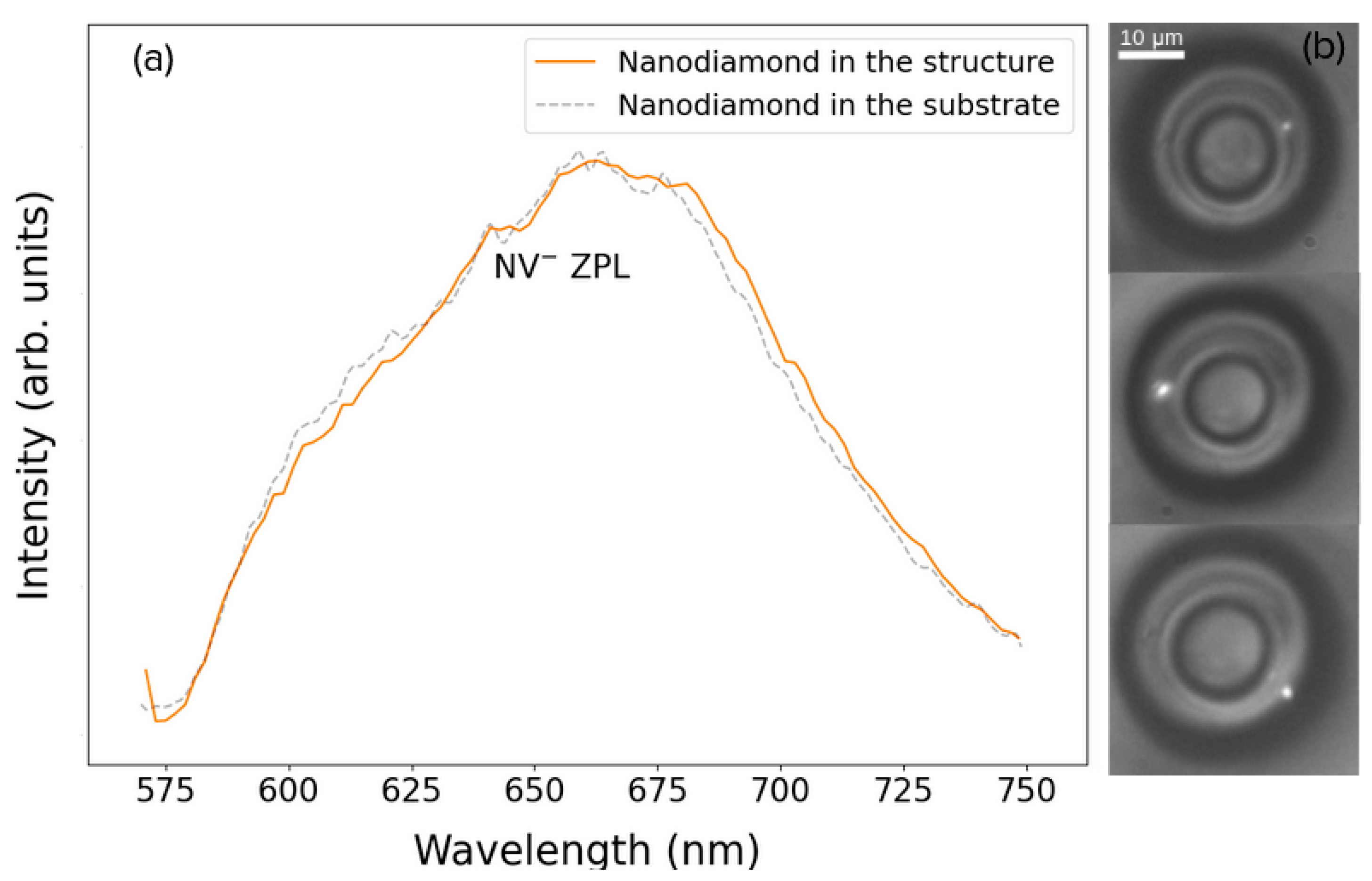
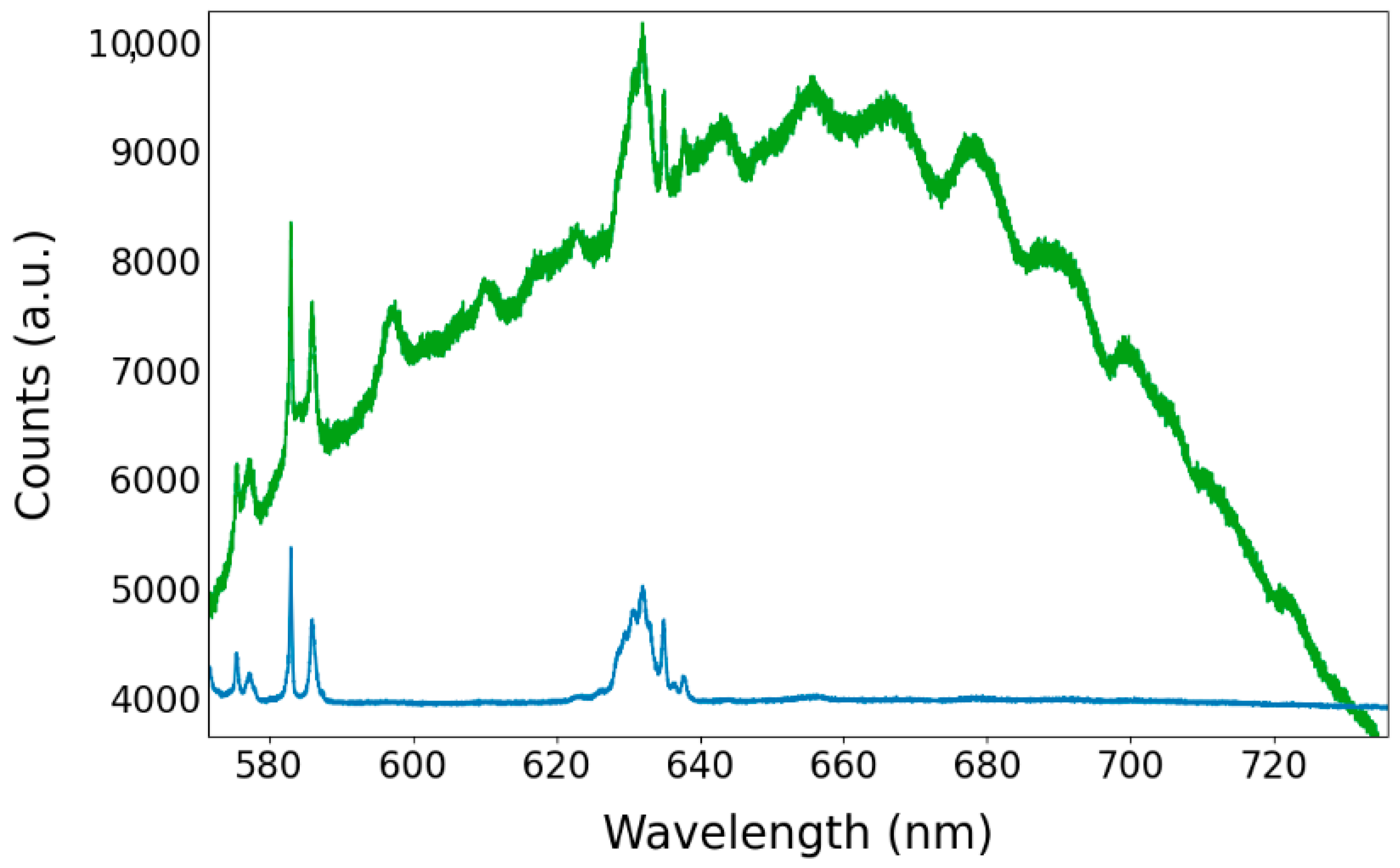
3. Results
4. Discussion
5. Conclusions
Author Contributions
Funding
Data Availability Statement
Acknowledgments
Conflicts of Interest
References
- Irber, D.M.; Poggiali, F.; Kong, F.; Kieschnick, M.; Lühmann, T.; Kwiatkowski, D.; Meijer, J.; Du, J.; Shi, F.; Reinhard, F. Robust all-optical single-shot readout of nitrogen-vacancy centers in diamond. Nat. Commun. 2021, 12, 532. [Google Scholar] [CrossRef]
- Kurtsiefer, C.; Mayer, S.; Zarda, P.; Weinfurter, H. Stable solid-state source of single photons. Phys. Rev. Lett. 2000, 85, 290. [Google Scholar] [CrossRef]
- Gruber, A.; Dräbenstedt, A.; Tietz, C.; Fleury, L.; Wrachtrup, J.; von Borczyskowski, C. Scanning confocal optical microscopy and magnetic resonance on single defect centers. Science 1997, 276, 2012–2014. [Google Scholar] [CrossRef]
- Zhang, T.; Pramanik, G.; Zhang, K.; Gulka, M.; Wang, L.; Jing, J.; Xu, F.; Li, Z.; Wei, Q.; Cigler, P.; et al. Toward Quantitative Bio-sensing with Nitrogen-Vacancy Center in Diamond. ACS Sens. 2021, 6, 2077–2107. [Google Scholar] [CrossRef]
- Wu, K.; Vedelaar, T.A.; Damle, V.G.; Morita, A.; Mougnaud, J.; Reyes San Martin, C.; Zhang, Y.; van der Pol, D.P.I.; Ende-Metselaar, H.; Rodenhuis-Zybert, I.; et al. Applying NV center-based quantum sensing to study intracellular free radical response upon viral infections. Redox Biol. 2022, 52, 102279. [Google Scholar] [CrossRef] [PubMed]
- Childress, L.; Gurudev Dutt, M.V.; Taylor, J.M.; Zibrov, A.S.; Jelezko, F.; Wrachtrup, J.; Hemmer, P.R.; Lukin, M.D. Coherent dynamics of coupled electron and nuclear spin qubits in diamond. Science 2006, 314, 281–285. [Google Scholar] [CrossRef]
- Waldherr, G.; Beck, J.; Steiner, M.; Neumann, P.; Gali, A.; Frauenheim, T.H.; Jelezko, F.; Wrachtrup, J. Dark states of single nitrogen-vacancy centers in diamond unraveled by single shot NMR. Phys. Rev. Lett. 2011, 106, 157601. [Google Scholar] [CrossRef]
- Xu, Z.; Yin, Z.; Han, Q.; Li, T. Quantum information processing with closely-spaced diamond color centers in strain and magnetic fields. Opt. Mater. Express 2019, 9, 4654–4668. [Google Scholar] [CrossRef]
- Santori, C.; Barclay, P.E.; Fu, K.M.C.; Beausoleil, R.G.; Spillane, S.; Fisch, M. Nanophotonics for quantum optics using nitrogen-vacancy centers in diamond. Nanotechnology 2010, 21, 274008. [Google Scholar] [CrossRef]
- Jung, T.; Görlitz, J.; Kambs, B.; Pauly, C.; Raatz, N.; Nelz, R.; Neu, E.; Edmonds, A.M.; Markham, M.; Mücklich, F.; et al. Spin measurements of NV centers coupled to a photonic crystal cavity. APL Photonics 2019, 4, 120803. [Google Scholar] [CrossRef]
- Vorobyov, V.V.; Soshenko, V.V.; Bolshedvorskii, S.V.; Javadzade, J.; Lebedev, N.; Smolyaninov, A.N.; Sorokin, V.N.; Akimov, A.V. Coupling of single NV Center to adiabatically tapered optical single mode fiber. Eur. Phys. J. D 2016, 70, 269. [Google Scholar] [CrossRef]
- Schröder, T.; Fujiwara, M.; Noda, T.; Zhao, H.-Q.; Benson, O.; Takeuchi, S.; Stick, D.; Hensinger, W.K.; Olmschenk, S.; Madsen, M.J.; et al. Quantum information processing and communication. Phys. Status Solidi A 2007, 318. [Google Scholar]
- Schietinger, S.; Schröder, T.; Benson, O. One-by-one coupling of single defect centers in nanodiamonds to high-Q modes of an optical microresonator. Nano Lett. 2008, 8, 3911–3915. [Google Scholar] [CrossRef] [PubMed]
- Schell, A.W.; Kaschke, J.; Fischer, J.; Henze, R.; Wolters, J.; Wegener, M.; Benson, O. Three-dimensional quantum photonic elements based on single nitrogen vacancy-centres in laser-written microstructures. Sci. Rep. 2013, 3, 1577. [Google Scholar] [CrossRef] [PubMed]
- Radulaski, M.; Zhang, J.L.; Tzeng, Y.K.; Lagoudakis, K.G.; Ishiwata, H.; Dory, C.; Fischer, K.A.; Kelaita, Y.A.; Sun, S.; Maurer, P.C.; et al. Nanodiamond Integration with Photonic Devices. Laser Photonics Rev. 2019, 13, 1800316. [Google Scholar] [CrossRef]
- Barclay, P.E.; Santori, C.; Fu, K.-M.; Beausoleil, R.G.; Painter, O. Coherent interference effects in a nano-assembled diamond NV center cavity-QED system. Opt. Express 2009, 17, 8081–8197. [Google Scholar] [CrossRef]
- Wolters, J.; Schell, A.W.; Kewes, G.; Nüsse, N.; Schoengen, M.; Döscher, H.; Hannappel, T.; Löchel, B.; Barth, M.; Benson, O. Enhancement of the zero phonon line emission from a single nitrogen vacancy center in a nanodiamond via coupling to a photonic crystal cavity. Appl. Phys. Lett. 2010, 97, 141108. [Google Scholar] [CrossRef]
- Serbin, J.; Ovsianikov, A.; Chichkov, B. Fabrication of woodpile structures by two-photon polymerization and investigation of their optical properties References and links. Opt. Express 2004, 12, 5221–5228. [Google Scholar] [CrossRef]
- Nocentini, S.; Riboli, F.; Burresi, M.; Martella, D.; Parmeggiani, C.; Wiersma, D.S. Three-Dimensional Photonic Circuits in Rigid and Soft Polymers Tunable by Light. ACS Photonics 2018, 5, 3222–3230. [Google Scholar] [CrossRef]
- Zhang, S.; Tang, S.J.; Feng, S.; Xiao, Y.F.; Cui, W.; Wang, X.; Sun, W.; Ye, J.; Han, P.; Zhang, X.; et al. High-Q Polymer Microcavities Integrated on a Multicore Fiber Facet for Vapor Sensing. Adv. Opt. Mater. 2019, 7, 1900602. [Google Scholar] [CrossRef]
- Gittard, S.D.; Ovsianikov, A.; Akar, H.; Chichkov, B.; Monteiro-Riviere, N.A.; Stafslien, S.; Chisholm, B.; Shin, C.C.; Shih, C.M.; Lin, S.J.; et al. Two photon polymerization-micromolding of polyethylene glycol-gentamicin sulfate microneedles. Adv. Eng. Mater. 2010, 12, B77–B82. [Google Scholar] [CrossRef] [PubMed]
- Otuka, A.J.G.; Tomazio, N.B.; Paula, K.T.; Mendonça, C.R. Two-photon polymerization: Functionalized microstructures, micro-resonators, and bio-scaffolds. Polymers 2021, 13, 1994. [Google Scholar] [CrossRef] [PubMed]
- Otuka, A.J.G.; Tribuzi, V.; Cardoso, M.R.; de Almeida, G.F.B.; Zanatta, A.R.; Corrêa, D.S.; Mendonça, C.R. Single-walled Carbon nanotubes functionalized with carboxylic acid for fabricating polymeric composite microstructures. J. Nanosci. Nanotechnol. 2015, 15, 9797–9801. [Google Scholar] [CrossRef] [PubMed]
- Tomazio, N.B.; de Boni, L.; Mendonca, C.R. Low threshold Rhodamine-doped whispering gallery mode microlasers fabricated by direct laser writing. Sci. Rep. 2017, 7, 8559. [Google Scholar] [CrossRef]
- Tomazio, N.B.; Paula, K.T.; Henrique, F.R.; Andrade, M.B.; Roselló-Mechó, X.; Delgado-Pinar, M.; Andrés, M.V.; Mendonca, C.R. Mode cleaning in graphene oxide-doped polymeric whispering gallery mode microresonators. J. Mater. Chem. C 2020, 8, 9707–9713. [Google Scholar] [CrossRef]
- Product Sheet Functionalized Fluorescent Nanodiamond. Available online: www.adamasnano.com (accessed on 26 November 2022).
- Knight, D.S.; White, W.B. Characterization of diamond films by Raman spectroscopy. J. Mater. Res. 1989, 4, 385–393. [Google Scholar] [CrossRef]


Disclaimer/Publisher’s Note: The statements, opinions and data contained in all publications are solely those of the individual author(s) and contributor(s) and not of MDPI and/or the editor(s). MDPI and/or the editor(s) disclaim responsibility for any injury to people or property resulting from any ideas, methods, instructions or products referred to in the content. |
© 2023 by the authors. Licensee MDPI, Basel, Switzerland. This article is an open access article distributed under the terms and conditions of the Creative Commons Attribution (CC BY) license (https://creativecommons.org/licenses/by/4.0/).
Share and Cite
Couto, F.A.; Andrade, M.B.; Otuka, A.J.G.; Pratavieira, S.; Muniz, S.R.; Mendonça, C.R. Integrating Fluorescent Nanodiamonds into Polymeric Microstructures Fabricated by Two-Photon Polymerization. Nanomaterials 2023, 13, 2571. https://doi.org/10.3390/nano13182571
Couto FA, Andrade MB, Otuka AJG, Pratavieira S, Muniz SR, Mendonça CR. Integrating Fluorescent Nanodiamonds into Polymeric Microstructures Fabricated by Two-Photon Polymerization. Nanomaterials. 2023; 13(18):2571. https://doi.org/10.3390/nano13182571
Chicago/Turabian StyleCouto, Filipe A., Marcelo B. Andrade, Adriano J. G. Otuka, Sebastião Pratavieira, Sergio R. Muniz, and Cleber R. Mendonça. 2023. "Integrating Fluorescent Nanodiamonds into Polymeric Microstructures Fabricated by Two-Photon Polymerization" Nanomaterials 13, no. 18: 2571. https://doi.org/10.3390/nano13182571
APA StyleCouto, F. A., Andrade, M. B., Otuka, A. J. G., Pratavieira, S., Muniz, S. R., & Mendonça, C. R. (2023). Integrating Fluorescent Nanodiamonds into Polymeric Microstructures Fabricated by Two-Photon Polymerization. Nanomaterials, 13(18), 2571. https://doi.org/10.3390/nano13182571