
Multi-Scale Femtosecond-Laser Texturing for Photothermal Efficiency Enhancement on Solar Absorbers Based on TaB2 Ceramics

 ,
,  ,
,  , and
, and
Abstract
1. Introduction
2. Materials and Methods
2.1. Ceramic Production
2.2. Surface Pattern Creation
2.3. Microstructure Characterization
2.4. Optical Characterization
3. Results
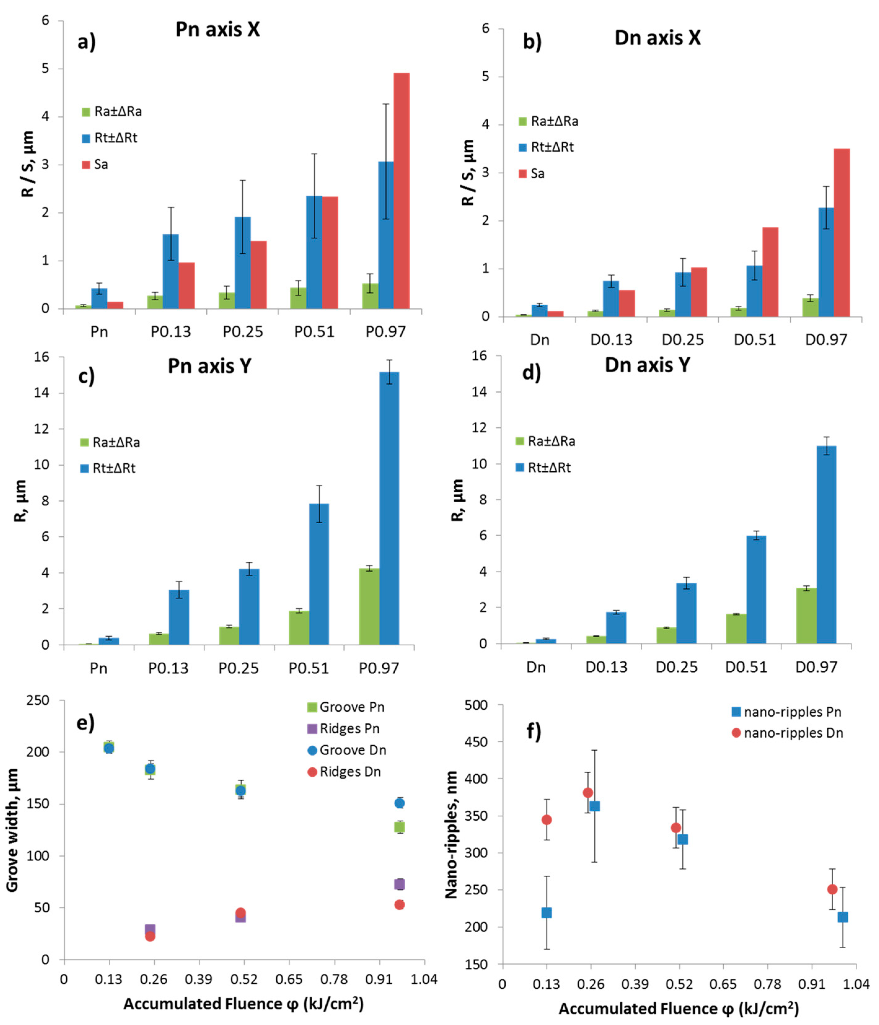
3.1. Microstructure
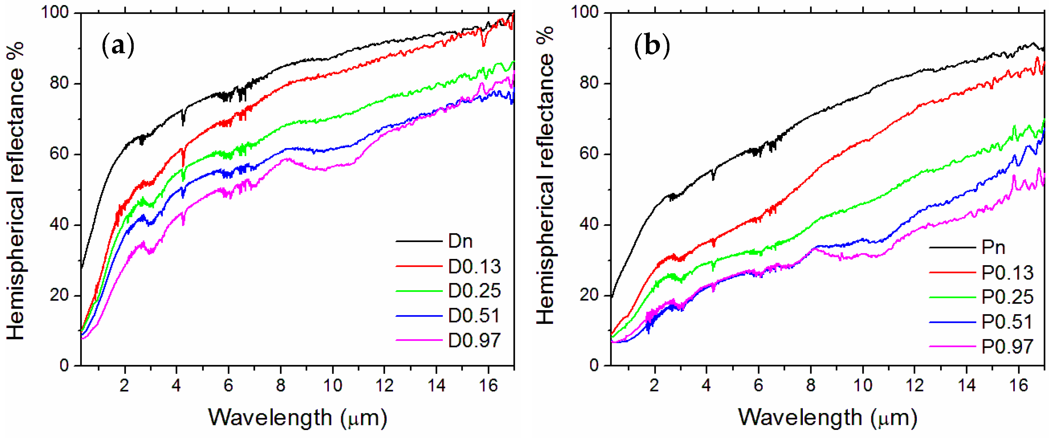
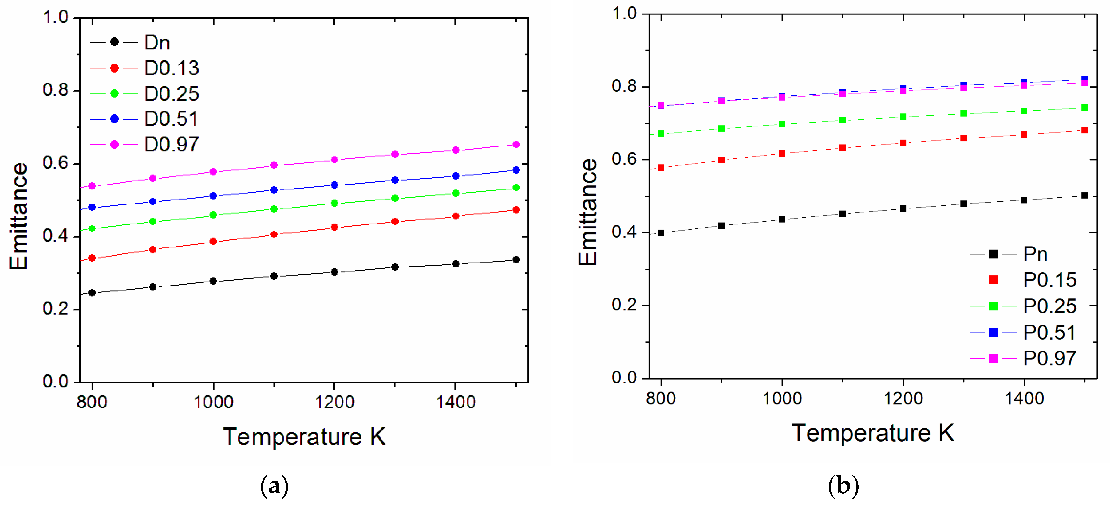
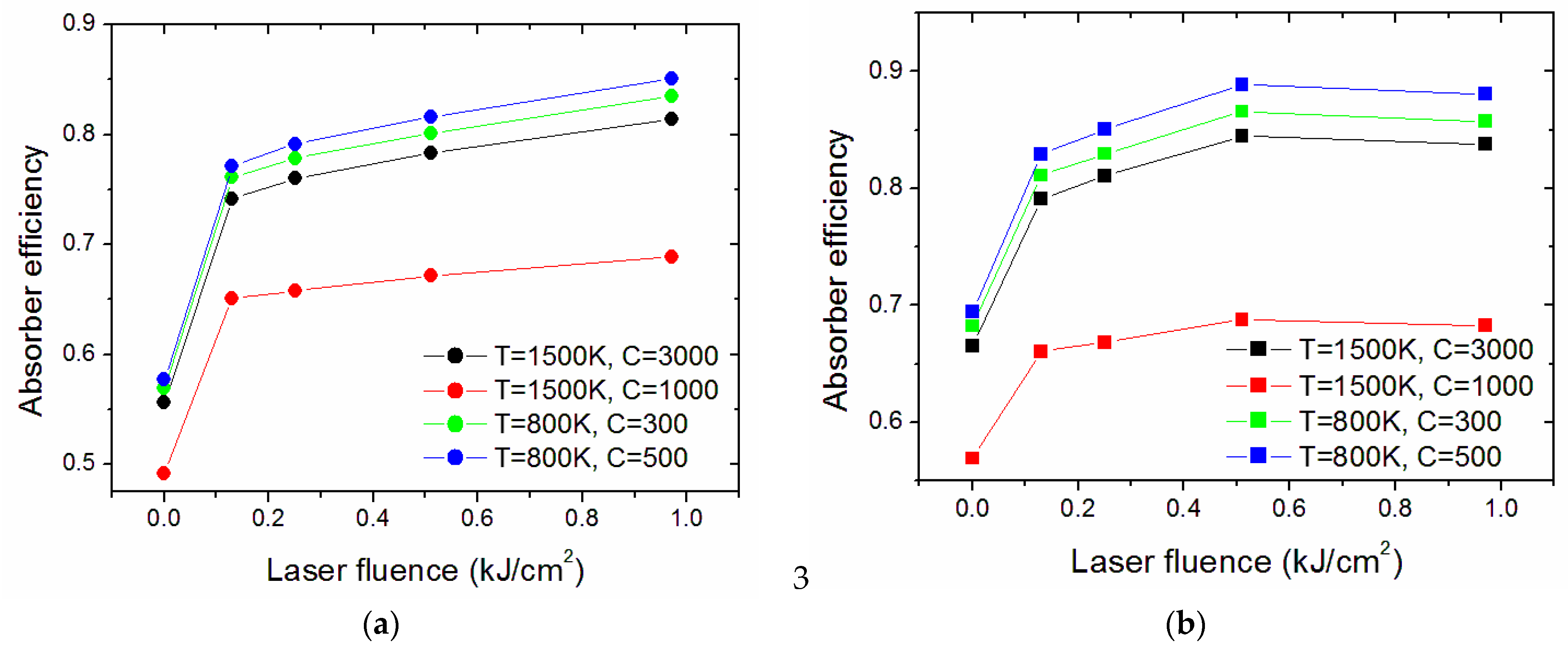
3.2. Optical Properties
4. Conclusions
Author Contributions
Funding
Data Availability Statement
Acknowledgments
Conflicts of Interest
References
- Thonig, R.; Lilliestam, J. Concentrating Solar Technology Policy Should Encourage High Temperatures and Modularity to Enable Spillovers. AIP Conf. Proc. 2021; in review. Available online: https://www.researchgate.net/publication/355154844 (accessed on 7 May 2023).
- World Energy Outlook 2021; International Energy Agency: Paris, France, 2022.
- ASTM G173-03; Standard Tables for Reference Solar Spectral Irradiances: Direct Normal and Hemispherical on 37° Tilted Surface. Active Standard ASTM G173. ASTM International: West Conshohocken, PA, USA, 2012.
- Nuru, Z.Y.; Motaung, D.E.; Kaviyarasu, K.; Maaza, M. Optimization and preparation of Pt–Al2O3 double cermet as selective solar absorber coatings. J. Alloys Compd. 2016, 664, 161–168. [Google Scholar] [CrossRef]
- Peterson, R.E.; Ramsey, J.W. Thin film coatings in solar—Thermal power systems. J. Vac. Sci. Technol. 1975, 12, 174–181. [Google Scholar] [CrossRef]
- Gao, H.; Peng, W.; Chu, S.; Cui, W.; Liu, Z.; Yu, L.; Jing, Z. Refractory ultra-broadband perfect absorber from visible to near-infrared. Nanomaterials 2018, 8, 1038. [Google Scholar] [CrossRef] [PubMed]
- Antonaia, A.; Castaldo, A.; Addonizio, M.L.; Esposito, S. Stability of W-Al2O3 cermet based solar coating for receiver tube operating at high temperature. Sol. Energy Mater. Sol. Cells 2010, 94, 1604–1611. [Google Scholar] [CrossRef]
- Cao, F.; Tang, L.; Li, Y.; Litvinchuk, A.P.; Bao, J.; Ren, Z. A high-temperature stable spectrally-selective solar absorber based on cermet of titanium nitride in SiO2 deposited on lanthanum aluminate. Sol. Energy Mater. Sol. Cells 2017, 160, 12–17. [Google Scholar] [CrossRef]
- Rodríguez-Palomo, A.; Céspedes, E.; Hernández-Pinilla, D.; Prieto, C. High-temperature air-stable solar selective coating based on MoSi2–Si3N4 composite. Sol. Energy Mater. Sol. Cells 2018, 174, 50–55. [Google Scholar] [CrossRef]
- Li, Y.; Li, D.; Zhou, D.; Chi, C.; Yang, S.; Huang, B. Efficient, Scalable, and High-Temperature Selective Solar Absorbers Based on Hybrid-Strategy Plasmonic Metamaterials. Sol. RRL 2018, 2, 1800057. [Google Scholar] [CrossRef]
- Cui, K.; Lemaire, P.; Zhao, H.; Savas, T.; Parsons, G.; Hart, A.J. Tungsten–carbon nanotube composite photonic crystals as thermally stable spectral-selective absorbers and emitters for thermophotovoltaics. Adv. Energy Mater. 2018, 8, 1801471. [Google Scholar] [CrossRef]
- Qiu, Y.; Xu, M.; Li, Q.; Huang, R.; Wang, J. A high-temperature near-perfect solar selective absorber combining tungsten nanohole and nanoshuriken arrays. ES Energy Environ. 2021, 13, 77–90. [Google Scholar] [CrossRef]
- Kim, M.S.; Lee, J.H.; Kwak, M.K. Surface texturing methods for solar cell efficiency enhancement. Int. J. Precis. Eng. Manuf. 2020, 21, 1389–1398. [Google Scholar] [CrossRef]
- Nikitin, P.; Zhukov, I.; Tkachev, D.; Kozulin, A.; Vorozhtsov, A. On the Tensile Strength of Spark Plasma Sintered AlMgB14 Ceramics. Nanomaterials 2022, 12, 3805. [Google Scholar] [CrossRef]
- Jeong, B.; Lahkar, S.; An, Q.; Reddy, K.M. Mechanical properties and deformation behavior of superhard lightweight nanocrystalline ceramics. Nanomaterials 2022, 12, 3228. [Google Scholar] [CrossRef] [PubMed]
- Sciti, D.; Silvestroni, L.; Trucchi, D.M.; Cappelli, E.; Orlando, S.; Sani, E. Femtosecond laser treatments to tailor the optical properties of hafnium carbide for solar applications. Sol. Energy Mater. Sol. Cells 2015, 132, 460–466. [Google Scholar] [CrossRef]
- Sciti, D.; Trucchi, D.M.; Bellucci, A.; Orlando, S.; Zoli, L.; Sani, E. Effect of surface texturing by femtosecond laser on tantalum carbide ceramics for solar receiver applications. Sol. Energy Mater. Sol. Cells 2017, 161, 1–6. [Google Scholar] [CrossRef]
- Sani, E.; Sciti, D.; Silvestroni, L.; Bellucci, A.; Orlando, S.; Trucchi, D.M. Tailoring optical properties of surfaces in wide spectral ranges by multi-scale femtosecond-laser texturing: A case-study for TaB2 ceramics. Opt. Mater. 2020, 109, 110347. [Google Scholar] [CrossRef]
- Sugioka, K.; Cheng, Y. Femtosecond laser three-dimensional micro-and nanofabrication. Appl. Phys. Rev. 2014, 1, 041303. [Google Scholar] [CrossRef]
- Gasch, M.J.; Ellerby, D.T.; Johnson, S.M. Ultra High Temperature Ceramic Composites. In Handbook of Ceramic Composites; Bansal, N.P., Ed.; Springer: Boston, MA, USA, 2005; pp. 197–224. [Google Scholar]
- Fahrenholtz, W.G.; Hilmas, G.E.; Talmy, I.G.; Zaykoski, J.A. Refractory diborides of zirconium and hafnium. J. Am. Ceram. Soc. 2007, 90, 1347–1364. [Google Scholar] [CrossRef]
- Sani, E.; Mercatelli, L.; Meucci, M.; Silvestroni, L.; Balbo, A.; Sciti, D. Process and composition dependence of optical properties of zirconium, hafnium and tantalum borides for solar receiver applications. Sol. Energy Mater. Sol. Cells 2016, 155, 368–377. [Google Scholar] [CrossRef]
- Sani, E.; Mercatelli, L.; Meucci, M.; Balbo, A.; Silvestroni, L.; Sciti, D. Compositional dependence of optical properties of zirconium, hafnium and tantalum carbides for solar absorber applications. Sol. Energy 2016, 131, 199–207. [Google Scholar] [CrossRef]
- Silvestroni, L.; Sciti, D.; Zoli, L.; Balbo, A.; Zanotto, F.; Orrù, R.; Licheri, R.; Musa, C.; Mercatelli, L.; Sani, E. An overview of ultra-refractory ceramics for thermodynamic solar energy generation at high temperature. Renew. Energy 2019, 133, 1257–1267. [Google Scholar] [CrossRef]
- Azzali, N.; Meucci, M.; Di Rosa, D.; Mercatelli, L.; Silvestroni, L.; Sciti, D.; Sani, E. Spectral emittance of ceramics for high temperature solar receivers. Sol. Energy 2021, 222, 74–83. [Google Scholar] [CrossRef]
- Sciti, D.; Silvestroni, L.; Sans, J.-L.; Mercatelli, L.; Meucci, M.; Sani, E. Tantalum diboride-based ceramics for bulk solar absorbers. Sol. Energy Mater. Sol. Cells 2014, 130, 208–216. [Google Scholar] [CrossRef]
- Silvestroni, L.; Guicciardi, S.; Melandri, C.; Sciti, D. TaB2-based ceramics: Microstructure, mechanical properties and oxidation resistance. J. Eur. Ceram. Soc. 2012, 32, 97–105. [Google Scholar] [CrossRef]
- Sciti, D.; Silvestroni, L.; Mercatelli, L.; Sans, J.L.; Sani, E. Suitability of ultra-refractory diboride ceramics as absorbers for solar energy applications. Sol. Energy Mater. Sol. Cells 2013, 109, 8–16. [Google Scholar] [CrossRef]
- Sani, E.; Mercatelli, L.; Sans, J.L.; Sciti, D. Optical properties of black and white ZrO2 for solar receiver applications. Sol. Energy Mater. Sol. Cells 2015, 140, 477. [Google Scholar] [CrossRef]
- Caron, S.; Garrido, J.; Ballestrín, J.; Sutter, F.; Röger, M.; Manzano-Agugliaro, F. A comparative analysis of opto-thermal figures of merit for high temperature solar thermal absorber coatings. Renew. Sustain. Energy Rev. 2022, 154, 111818. [Google Scholar] [CrossRef]
- Florian, C.; Kirner, S.V.; Krüger, J.; Bonse, J. Surface functionalization by laser-induced periodic surface structures. J. Laser Appl. 2020, 32, 022063. [Google Scholar] [CrossRef]
- Girolami, M.; Bellucci, A.; Mastellone, M.; Orlando, S.; Serpente, V.; Valentini, V.; Polini, R.; Sani, E.; De Caro, T.; Trucchi, D.M. Femtosecond-Laser Nanostructuring of Black Diamond Films under Different Gas Environments. Materials 2020, 13, 5761. [Google Scholar] [CrossRef] [PubMed]
- Licheri, R.; Musa, C.; Locci, A.M.; Montinaro, S.; Orrù, R.; Cao, G.; Silvestroni, L.; Sciti, D.; Azzali, N.; Mercatelli, L.; et al. Ultra-high temperature porous graded ceramics for solar energy applications. J. Eur. Ceram. Soc. 2018, 39, 72–78. [Google Scholar] [CrossRef]
- Sani, E.; Mercatelli, L.; Sans, J.L.; Silvestroni, L.; Sciti, D. Porous and dense hafnium and zirconium ultra-high temperature ceramics for solar receivers. Opt. Mater. 2013, 36, 163–168. [Google Scholar] [CrossRef]
- Duffie, J.A.; Beckman, W.A. Solar Engineering of Thermal Processes; John Wiley & Sons: Hoboken, NJ, USA, 1991. [Google Scholar]
- Belgasim, B.; Aldali, Y.; Abdunnabi, M.J.; Hashem, G.; Hossin, K. The potential of concentrating solar power (CSP) for electricity generation in Libya. Renew. Sustain. Energy Rev. 2018, 90, 1–15. [Google Scholar] [CrossRef]


| Sample Label @ 80% Density | Sample Label @ 100% Density | x-Scanning Speed (μm/s) | Accumulated Laser Fluence ϕ (kJ/cm2) |
|---|---|---|---|
| Pn | Dn | -- | 0 |
| P0.13 | D0.13 | 5000 | 0.13 |
| P0.25 | D0.25 | 2500 | 0.25 |
| P0.51 | D0.51 | 1250 | 0.51 |
| P0.97 | D0.97 | 625 | 0.97 |
Disclaimer/Publisher’s Note: The statements, opinions and data contained in all publications are solely those of the individual author(s) and contributor(s) and not of MDPI and/or the editor(s). MDPI and/or the editor(s) disclaim responsibility for any injury to people or property resulting from any ideas, methods, instructions or products referred to in the content. |
© 2023 by the authors. Licensee MDPI, Basel, Switzerland. This article is an open access article distributed under the terms and conditions of the Creative Commons Attribution (CC BY) license (https://creativecommons.org/licenses/by/4.0/).
Share and Cite
Sani, E.; Sciti, D.; Failla, S.; Melandri, C.; Bellucci, A.; Orlando, S.; Trucchi, D.M. Multi-Scale Femtosecond-Laser Texturing for Photothermal Efficiency Enhancement on Solar Absorbers Based on TaB2 Ceramics. Nanomaterials 2023, 13, 1692. https://doi.org/10.3390/nano13101692
Sani E, Sciti D, Failla S, Melandri C, Bellucci A, Orlando S, Trucchi DM. Multi-Scale Femtosecond-Laser Texturing for Photothermal Efficiency Enhancement on Solar Absorbers Based on TaB2 Ceramics. Nanomaterials. 2023; 13(10):1692. https://doi.org/10.3390/nano13101692
Chicago/Turabian StyleSani, Elisa, Diletta Sciti, Simone Failla, Cesare Melandri, Alessandro Bellucci, Stefano Orlando, and Daniele M. Trucchi. 2023. "Multi-Scale Femtosecond-Laser Texturing for Photothermal Efficiency Enhancement on Solar Absorbers Based on TaB2 Ceramics" Nanomaterials 13, no. 10: 1692. https://doi.org/10.3390/nano13101692
APA StyleSani, E., Sciti, D., Failla, S., Melandri, C., Bellucci, A., Orlando, S., & Trucchi, D. M. (2023). Multi-Scale Femtosecond-Laser Texturing for Photothermal Efficiency Enhancement on Solar Absorbers Based on TaB2 Ceramics. Nanomaterials, 13(10), 1692. https://doi.org/10.3390/nano13101692