Article

Numerical Investigation of Photo-Generated Carrier Recombination Dynamics on the Device Characteristics for the Perovskite/Carbon Nitride Absorber-Layer Solar Cell

1
Functional Materials and Optoelectronic Devices (FMOD) Lab, Department of Physics, Lahore University of Management Sciences (LUMS), Lahore 54792, Pakistan
2
Department of Electrical Engineering, Lahore University of Management Sciences (LUMS), Lahore 54792, Pakistan
3
Department of Electrical Engineering, University of Engineering and Technology Lahore, Lahore 39161, Pakistan
4
Department of Electrical Engineering, University of Lahore, Lahore 54590, Pakistan
5
ENET Centre, VSB—Technical University of Ostrava, 708 00 Ostrava, Czech Republic
6
Department of Electrical Engineering, College of Engineering, Taif University, P.O. Box 11099, Taif 21944, Saudi Arabia
*
Authors to whom correspondence should be addressed.
Nanomaterials 2022, 12(22), 4012; https://doi.org/10.3390/nano12224012
Submission received: 7 October 2022 / Revised: 2 November 2022 / Accepted: 9 November 2022 / Published: 15 November 2022

Abstract

:
The nitrogenated holey two-dimensional carbon nitride ( C 2 N ) has been efficaciously utilized in the fabrication of transistors, sensors, and batteries in recent years, but lacks application in the photovoltaic industry. The C 2 N possesses favorable optoelectronic properties. To investigate its potential feasibility for solar cells (as either an absorber layer/interface layer), we foremost detailed the numerical modeling of the double-absorber-layer–methyl ammonium lead iodide ( CH 3 NH 3 PbI 3 ) –carbon nitride ( C 2 N ) layer solar cell and subsequently provided in-depth insight into the active-layer-associated recombination losses limiting the efficiency ( η ) of the solar cell. Under the recombination kinetics phenomena, we explored the influence of radiative recombination, Auger recombination, Shockley Read Hall recombination, the energy distribution of defects, Band Tail recombination (Hoping Model), Gaussian distribution, and metastable defect states, including single-donor (0/+), single-acceptor (−/0), double-donor (0/+/2+), double-acceptor (2/−/0−), and the interface-layer defects on the output characteristics of the solar cell. Setting the defect (or trap) density to 10 15 cm 3 with a uniform energy distribution of defects for all layers, we achieved an   η of 24.16%. A considerable enhancement in power-conversion efficiency (   η ~ 27 % ) was perceived as we reduced the trap density to 10 14 cm 3 for the absorber layers. Furthermore, it was observed that, for the absorber layer with double-donor defect states, the active layer should be carefully synthesized to reduce crystal-order defects to keep the total defect density as low as 10 17 cm 3 to achieve efficient device characteristics.

1. Introduction

At present, photovoltaic modules based on wafer-based crystalline silicon solar cells account for >90% of the global photovoltaic market [1,2,3,4,5]. Laudable enhancements in power conversion efficiency ( η ) have been experienced for this technology over the last few years, leading to thin film, tandem, and various lab-based architectures [6,7,8,9,10,11,12,13]. Additionally, the manufacturing process of crystalline-based solar modules requires expensive materials and high production costs. Given that, double-absorber-layer (DAL) solar cells, rivaling the tandem solar cells, can be considered a promising candidate, among emerging photovoltaic technology, achieving a high device performance while cutting costs [14].
Despite perceptible advancements in tandem solar cells (perovskite/silicon tandem solar cells that have been reported recently, with an impressive η ~ 29.15 % [15]), the ease of fabricating DAL solar cells is one of the major advantages reducing complexity in tuning two-terminal tandem solar cells or managing the four-terminal tandem device circuitry. Besides this, DAL solar cells can be characterized by low production costs, compared to tandem solar cells, making them a potential candidate for the future of the photovoltaic industry [16].
The composition of DAL solar cells requires the absorber layers (or active layers) to have an almost similar lattice structure [16]. The active layers can be chalcogenides, perovskites, polymers, or other organic/inorganic layers. In such an architecture, the absorber layer with varied energy band gaps, which form the junctions sequentially, harness photo-generated power from their respective portions of the solar spectrum. This makes the multi-junction devices efficient and comparable to single-junction ones. However, the success of such DAL devices lies in the current matching of the active-layer junctions and efficient recombination of photo-generated carriers from the adjacent junctions.
To date, limited research has reported on the theoretical modeling/fabrication of DAL solar cells. Ho Yeon, Deuk, et al. [17] reported a 4% efficient PbS/Cds solar cell fabricated by chemical bath deposition. Ahmad, Faiz et al. [14] theoretically proposed an optical modeling of a CuIn 1 ξ 1 Ga ξ 1 Se 2 / Cu 2 ZnSn ( S ξ 2 Se 1 ξ 2 ) absorber layer solar cell with an impressive η ~ 34.45 % . AlZoubi, Tariq, et al. [18] detailed a numerical modeling of a CZTS/Si-based active layer solar cell with η   ~ 29.15 % . Maurya, K et al. [19] computationally detailed a >35% efficient thin-film device based on an Sb 2 Se 3 /CZTS absorber layer. S Yasin et al. [16] recently detailed a C 2 N / FASnI 3 absorber layer solar cell with η   ~ 25.15 % , keeping the trap density at 10 14 cm 3 .
Here, we proposed a novel structured DAL, employing metal halide perovskite and Carbon Nitride ( C 2 N ) as the absorber layers. Carbon Nitride ( C 2 N ) is a 2D material with a structural composition similar to graphene, with a wider energy band gap ~   1.8   eV , and a higher optical absorption in the visible spectrum. C 2 N has been used for photocatalysis, and in the fabrication of field effect transistors FETs, biosensors, batteries, and hydrogen storing [20,21,22,23]. C 2 N material has favorable properties for use as a primary absorber for photovoltaic applications. It has been numerically explored for photovoltaic cell modeling but has not yet been reported in the literature. We, therefore, focused on a defect-based study for the absorber layers, to comprehensively investigate the proposed active layered structure solar cell favorability for future thin-film photovoltaic applications.

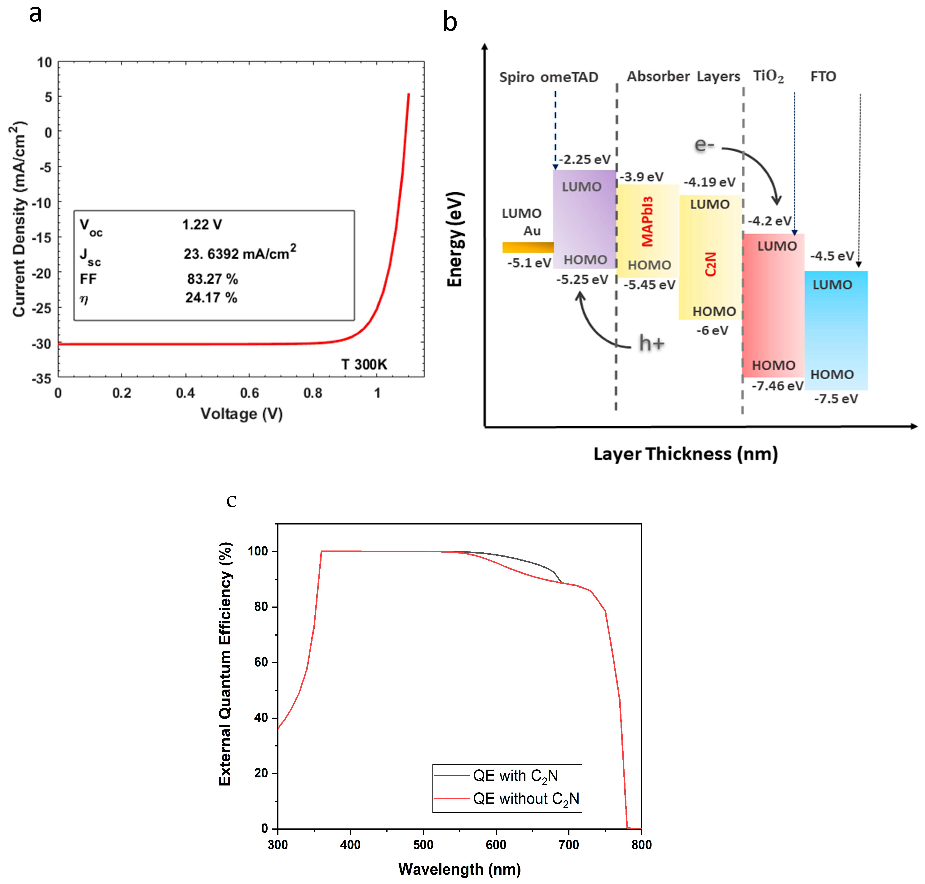
2. Numerical Modeling and Material Parameters

The proposed solar cell is composed of FTO/ TiO 2 / C 2 N / CH 3 NH 3 PbI 3 /SpiroOmeTAD/Au-back metal contact (see Figure 1) and was numerically modeled and investigated in SCAPS-1D, which is based on three coupled semiconductor differential equations: Poisson’s equation, and the continuity equations for electrons and holes (1) [7]. The material parameters for the simulation are enlisted in Appendix A Table A1. The SCAPS numerically evaluates the steady-state solution of these equations with appropriate boundary conditions [24,25,26,27].
{   2 V   ( x ) = q ε [ p ( x ) n ( x ) + N D + ( x ) N A ( x ) + N t r ± ] p ( n ) t = G p ( x ) p n p n o τ p p n μ p d ξ d x + μ p ξ d p n d x + D p d 2 p n d x 2 d n p d t = G n ( x ) n p n p o τ n n p μ n d ξ d x + μ n ξ d n p d x + D n d 2 n p d x 2  
where 2 V is the electrostatic potential, q is the electronic charge, p ( x ) and n ( x ) are the position-dependent hole and electron concentration, N D + ( x ) and N A ( x ) is the position-dependent ionized dopant and acceptor concentration, N t r ± is the shallow/bulk trap (or defect) carrier concentration. The electron–hole pair generation, G ( x ) in the absorber layer is a result of incident photon flux ( N p h o t ) of wavelength ( λ ), at each position ( x ) within the layer, and follows the mathematical relation (2) [28]. λ m i n ,   λ m a x are the minimum and maximum wavelengths of the incoming solar spectrum.
G ( λ , x ) = α ( ( λ , x ) ) . N p h o t ( λ , x ) = λ m i n   λ m a x G ( λ , x )   d λ = λ m i n   λ m a x α ( ( λ , x ) ) . N p h o t ( λ , x ) d λ
where, in
N p h o t ( λ , x ) = N p h o t 0 ( λ ) . T f r o n t ( λ ) . exp ( x α ( λ ) ) . 1 + R b a c k ( λ ) exp ( 2 ( d x ) α ( λ ) ) 1 R b a c k ( λ ) R i n t exp ( 2 d α ( λ ) )
In the above equation, T f r o n t ( λ ) is the transmission at the front contact (wavelength-dependent), R b a c k ( λ ) is the reflection at the back contact (wavelength-dependent), R i n t is the internal reflection at the front contact, and d is the layer thickness.
Further, we employed one of the four SCAPS inbuilt optical absorption ( α ) models following the expression (4) [28]. In this model energy band gap, ( E g ) follows the square root law and α = 0 if the incident photon energy is < E g .
α ( h v ) = ( α o + β o E g h v ) h v E g 1  
The device with only the perovskite absorber layer demonstrated an η of 23.83%, an open-circuit voltage ( V o c ) of 1.22 V, a short circuit current density ( J s c ) of 23.3418 mA / cm 2 ,   and a fill factor (FF) of 83.18%. The devices with optimized thicknesses with perovskite/ C 2 N demonstrated an increased η of 24.17%, an open-circuit voltage ( V o c ) of 1.22 V, a short circuit current density ( J s c ) of 23.6392 mA / cm 2 , and a fill factor (FF) of 83.27%. The current density–voltage curve of the DAL solar, under standard illumination conditions, is depicted in Figure 2a. Figure 2b illustrates the energy level diagram of the solar cell. Furthermore, the external quantum efficiency of the solar cell with C 2 N (see Figure 2c) remained at > 90% for the near-ultraviolet region, ( 360   nm   incident light   360   nm or photon energy, E p ~3.44 eV) to the major part of the visible-light spectrum (incident light wavelengths 360   nm or E p ~3.44 eV), clearly showing a better quantum efficiency response than a single-absorber layer. It should be noted that, in further sections, defects are simultaneously introduced/changed in perovskite/carbon nitride absorber layers for investigation into the impact of the recombination phenomenon on device performance.

3. Results and Discussion

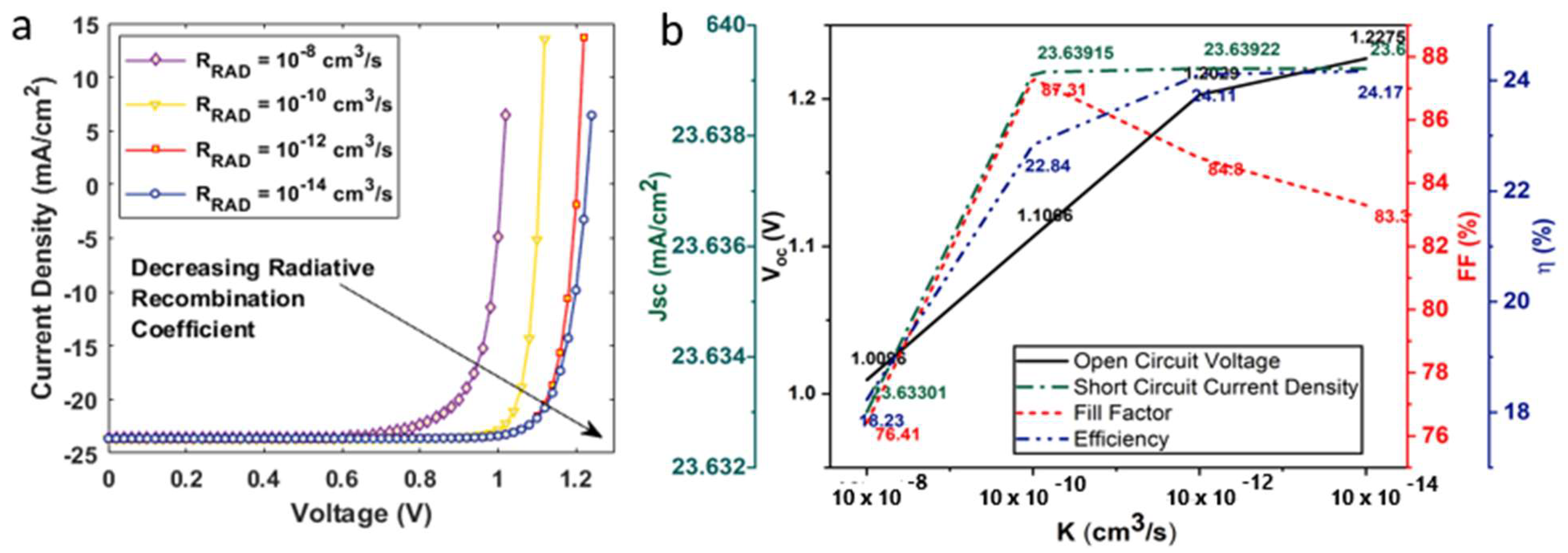
3.1. Influence of Recombination on Device Performance

Ideally, photovoltaic material has a higher absorption coefficient to effectively harvest incident solar energy photons and convert them into free charge carriers. However, recombination losses in solar cells are inevitable due to material defects [29]. Recombination losses affect the collection current, as well as the forward-bias injection current. This directly influences the short-circuit current density and open-circuit voltage of the solar cell, thereby limiting the fill factor and efficiency of the solar cell [30]. Recombination mechanisms considered in this investigation for the CH 3 NH 3 PbI 3 / C 2 N absorber layer include radiative recombination ( R R a d ), Auger ( R A u g ) and Shockley Read Hall recombination ( R S R H ), following expression (5). More insight into the recombination phenomenon is provided in Figure 3.
{ R = R R a d + R A u g + R S R H     R R a d = K   ( n p n i 2 )     R A u g = ( C n , a u g n + C n , a u g p ) ( n p n i 2 )   R S R H = ( n p n i 2 ) τ p   ( n + n i exp ( E t E i k T ) ) + τ n   ( p + n i exp ( E i E t k T ) )  
where K is the radiative recombination coefficient, C n A   ( C p A ) is the Auger electron (hole) recombination coefficient, n   ( p ) is the electron (hole) carrier concentration, τ n ( τ p ) is the electron (hole) carrier lifetime, E i is the intrinsic energy level, E t is the trap energy level, and T is the temperature at room temperature. The K factor for CH 3 NH 3 PbI 3 , as calculated by the first principles, is reported in the range of (0.5–1.5)   ×   10 9   ( cm 3 / s ) . The range of C n A   ( C p A T h e ) factor for CH 3 NH 3 PbI 3 perovskite material, as evaluated from time- and excitation-energy-dependent photoluminescence spectroscopy, has been reported to lie between 1.8 and 3.7. The point defect study on C 2 N confirmed that such materials exhibit both a direct and indirect energy bandgap nature. We therefore set similar K and C n A   ( C p A T h e ) factors for both the absorber layers. The device’s current density voltage characteristics under radiative, Auger, and SRH recombination are shown in Figure 4a, Figure 5a and Figure 6a, respectively.
To investigate the impact of radiative recombination, we varied the K factor in the range of 10 8 10 14   ( cm 3 / s ) (see Figure 4b). An increased value of K has an adverse effect on the output characteristics of the solar cell. It was observed that the device demonstrated a maximum η ~24.17%, V o c   ~   1.22   V , and J s c   ~ 23.64   mA / cm 2 at K = 10 14   cm 3 / s , as illustrated in Figure 4. The highest FF ~ 87.31 % was obtained at K = 10 10   cm 3 / s . The device’s η fell to ~16% as we increased the K to 10 8   c m 3 / s . To investigate the influence of R A u g on device performance, we varied the C n , a u g ( C p , a u g ) at 10 25 10 31   ( cm 6 / s ) (see Figure 5). The device demonstrated a maximum η at C n , a u g = 10 31   cm 6 / s and a minimum C n , a u g = 10 25   cm 6 / s . To analyze R S R H , we employed the trap density model as it has been elaborated in previous studies. The trap density for the double-absorber layer, N t r , D A L was within the range 10 14 10 17   cm 3 (see Figure 6). As discussed earlier, the device was simulated with a defect density of 10 15   cm 3 . On decreasing the defect density to 10 14   cm 3 , the device demonstrated a maximum η ~26.18%, V o c   ~   1.34   V , and J s c   ~ 26.79   mA / cm 2 , and the device η reduced to ~17%, including other device parameters, as we increased the defect density to 10 17   cm 3 .

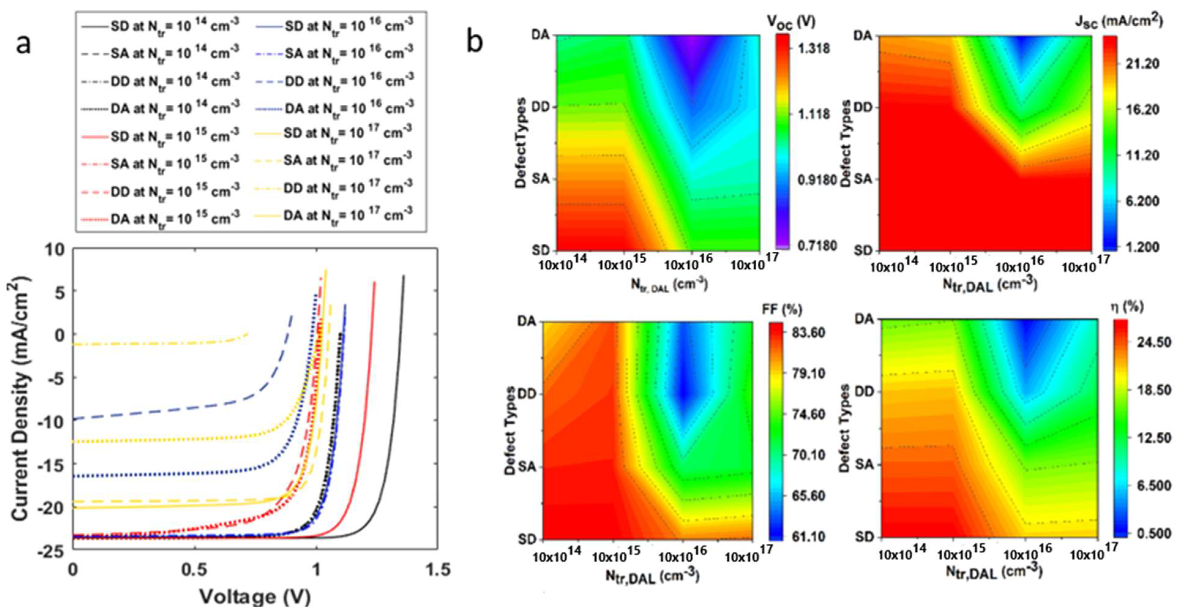
3.2. Influence of Energy Distribution of Defects on the Device Performance

In organic–inorganic absorber layers, the energy distribution of defect modeling is imperative to accurately model the device. The total defect density of state (DOS) in the absorber layer is assumed to comprise shallow level defects, modeled by exponentially decaying conduction or valence band tail states, and deep-level defects modeled by Gaussian distribution in the mid-gaps (see Figure 7a) [31,32]. The Gaussian conduction/valence band tail state, and energy distribution in the SCAPS environment follow the mathematical relation (6–8) [28] where E t is the tap energy level, E c is the characteristic energy, w G is the width of Gaussian energy distribution, w t is the width of tail-like distribution, N t ( E ) is the defect density in cm 3 / eV , and N p e a k is the peak density of the energy distribution. Band tailing hampers the mobility of photo-generated carriers to a great extent by trapping and de-trapping. The w G ( o r   w t ) is related to the degree of disorder in crystals [33]. Experimentally reported values for perovskite material are in the range of 15 63   ( meV ) [34].
However, we kept the w G as 0.564 eV, while w t = 0.1 eV for the absorber layers. The N p e a k in all the above-mentioned energy distributions is 10 15   ( 1 / eV / cm 3 ) , with total defect density states of 10 15   cm 3 .
R a n g e = [ E t w G E c 2 ; E t + w G E c 2 ] ,   N t ( E ) = N p e a k × exp [ ( E E t   E c ) 2 ]   G a u s s i a n   E n e r g y   D i s t r i b u t i o n
R a n g e = [ E t w t E c ; E t ] ,   N t ( E ) = N p e a k × exp [ E E t E c ]   C o n d u c t i o n   B a n d   E n e r g y   D i s t r i b u t i o n  
R a n g e = [ E t ; E t + w t E c ] ,   N t ( E ) = N p e a k × exp [ E E t E c ]   V a l e n c e   B a n d   E n e r g y   D i s t r i b u t i o n
The device was simulated with the above modeling, and current density vs. voltage characteristics are shown in Figure 7b. the device η   was decreased to 22.12% from 24.17%, V o c to ~ 1.14 V, J s c to ~ 23.634 mA / cm 2 , and FF ~ 81 as can be observed in the figure. The current density curve under both conditions is summarized in Table 1.

3.3. Influence of Metastable Defects on the Device Performance

In this section, we investigated the impact of metastable defect transition on the absorber layers. In CH 3 NH 3 PbI 3 , halide ion segregation requires the migration of halide ions, which is a defect-driven process resulting in halide vacancy defects [35]. For the absorber layer, we induced double-vacancy defects, including a single donor ( S D ( 0 / + ) ), double acceptor ( S D ( / 0 ) ), double donor ( D D ( 0 / + / 2 / + ) ), and double acceptor ( D A ( 2 / / 0 / ) ), at varying total trap densities. The single (double)-donor defect states per unit of volume are concentrated closer to the conduction band edge, while single (double) acceptors are concentrated closer to the valence band [36,37]. The impact of metastable defects on device output characteristics at varied trap densities ( 10 14 10 17   cm 3 ) is summarized in Table 2, Table 3, Table 4 and Table 5. It was observed that single-donor defects affected the device output characteristics the least. However, the D D ( 0 / + / 2 / + ) defect considerably affected solar cell performance in all conditions. The current density voltage characteristics for metastable state defects are depicted in Figure 8a, while Figure 8b provides more insight into the results.

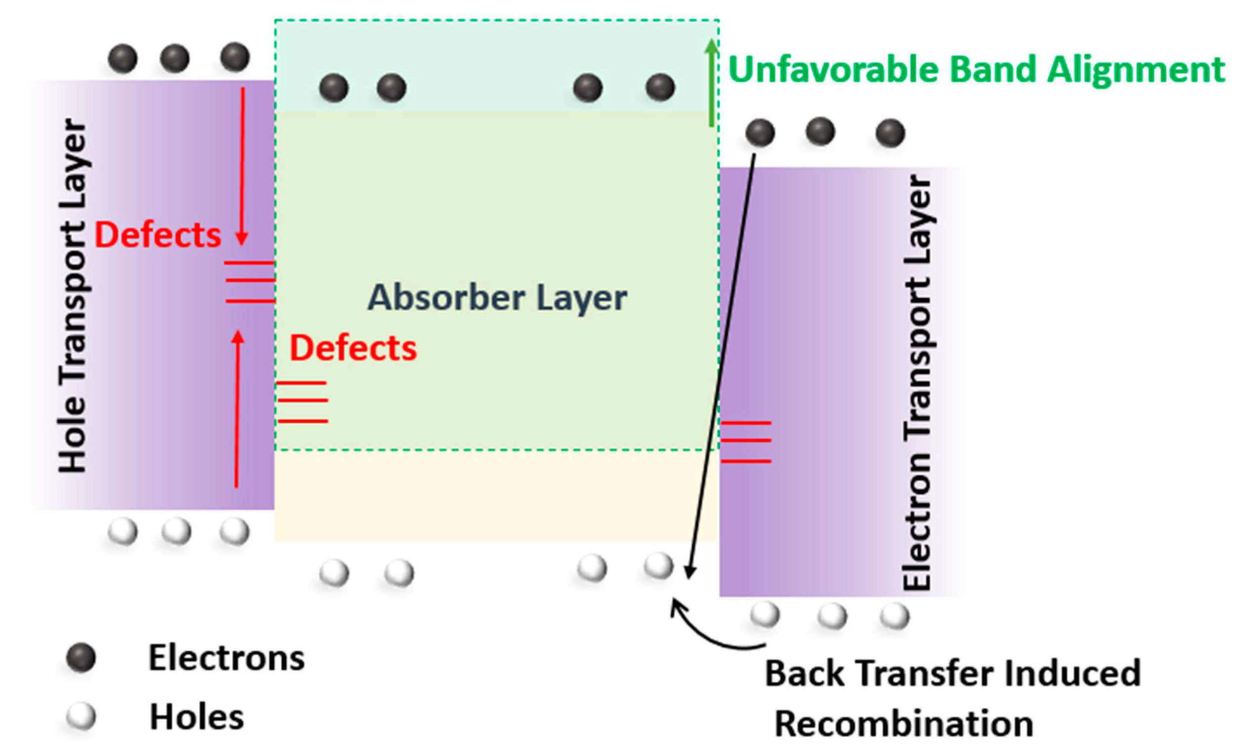
3.4. Influence of Interface Defects on the Device Performance

Interfacial recombination plays a significant role in determining the performance of the solar cell. Interface defects emerge due to recombination centers at the interface of the absorber material/hole-transport layer (or electron-transport layer) [38]. These recombination centers can be present inside the absorber layer or hole-transport layer (or electron-transport layer), at the interface. Other reasons for interface defects can be an unfavorable HTL/absorber layer (or absorber layer/ETL), band alignment, and back-transfer-induced recombination [39], as illustrated in Figure 9.
The current density–voltage curve shown in Figure 10a illustrates the effect of varying interface defect densities at the hole transport layer/absorber layer interface, N t r , H / A . The N t r , H / A was varied in the range of 10 14 10 17   ( cm 3 ). Interface defects considerably affected the device power conversion efficiency of the solar cell, in comparison to J s c , V o c ,   F F , as can be observed from Figure 10b. At N t r , H / A = 10 14   cm 3 , the device η was 23.19% and was decreased to 18.24% at N t r , H / A = 10 14   cm 3 , indicating high recombination at the interface (Figure 11). Similarly, interface defect density at the absorber layer/electron transport layer interface, N t r , A / E . was also varied in the range of 10 14 10 17   ( cm 3 ). Unlike N t r , H / A , N t r , A / E did not significantly affect the device performance. The device η , V o c , FF, and J s c retained their initial optimized values at N t r , A / E of 10 14 10 16   cm 3 . However, η fell slightly to 23.83%, from 24.17%, on a further increase in interface defects.

4. Conclusions

The combination of two absorber layers, carbon nitride and a perovskite absorber layer, aided in the utilization of a broader range of solar spectrum for solar energy conversion. The device demonstrated high efficiency (24.17%), open-circuit voltage (1.2 V), and fill factor (83.2%), with a uniform DOS energy bandgap. However, the focus was on the computational investigation of dominant recombination mechanisms associated with the absorber layer, to accurately investigate the device performance. The device η remained > 16% under higher radiative, auger coefficient, and trap-assisted recombination. Thereafter, we modeled the Gaussian distribution energy profile for shallow-level defects and Urbach tail states for shallow-level defects. This resulted in device efficiency falling to 22.14%. Further, various double-vacancy-based metastable defect states were induced in the absorber layer. It was observed that double-donor metastable defects highly affected the performance of the solar cell. Finally, we also investigated the influence of interface defects. It was revealed that. for the proposed device architecture, increased defects in the HTL/absorber layer dominantly affected the device performance, instead of absorber-layer/ETL interface defects.

Author Contributions

Conceptualization, F.S.; Formal analysis, F.S., M.H.K., H.A.T. and S.M.S.; Funding acquisition, L.P., V.B., S.M. and N.U.; Investigation, F.S., A.H. and A.I.; Methodology, F.S., H.A.T. and A.H.; Software, F.S.; Writing—original draft, F.S.; Writing—review and editing, L.P., V.B. and N.U. All authors have read and agreed to the published version of the manuscript.

Funding

This paper received funds from the following projects: The Doctoral grant competition VSB—Technical University of Ostrava, reg. no. CZ.02.2.69/0.0/0.0/19 073/0016945 within the Operational Programme Research, Development and Education, under project DGS/TEAM/2020-017 “Smart Control System for Energy Flow Optimization and Management in a Microgrid with V2H/V2G Technology” and project TN01000007 National Centre for Energy.

Data Availability Statement

Not applicable.

Acknowledgments

This paper was supported by the following projects: The Doctoral grant competition VSB—Technical University of Ostrava, reg. no. CZ.02.2.69/0.0/0.0/19 073/0016945 within the Operational Programme Research, Development and Education, under project DGS/TEAM/2020-017 “Smart Control System for Energy Flow Optimization and Management in a Microgrid with V2H/V2G Technology” and project TN01000007 National Centre for Energy.

Conflicts of Interest

The authors declare no conflict of interest.

Nomenclature

η Efficiency
V o c Open Circuit Voltage
J s c Short-Circuit Current Density
FFFill Factor
HTLHole transport Layer
ETLElectron Transport Layer
DALDouble Absorber Layer
λ Wavelength
p ( x ) Position-dependent hole concentration
n ( x ) Position-dependent electron concentration
N t r ± Shallow/bulk carrier concentration
GElectron–hole pair generation
λ m i n Minimum wavelength
λ m a x Maximum wavelength
T f r o n t ( λ ) Transmission at front contact dependent on wavelength
R b a c k ( λ ) Reflection at back contact dependent on wavelength
R i n t ( λ ) Internal reflection at front contact
DLayer thickness
E g Energy bandgap
α Optical absorption
E p Photon energy
R R A D Radiative recombination
R A U G Auger recombination
R S R H Schokley Read hall recombination
KRadiative recombination coefficient
C n , a u g Auger–electron recombination coefficient
C p , a u g Auger–hole recombination coefficient
n Electron concentration
p Hole concentration
n i Intrinsic-carrier concentration
τ n Electron-carrier lifetime
τ p Hole-carrier lifetime
N t r , D A L Trap density of double absorber layer
E c Characteristic energy
w g Width of Gaussian energy distribution
w t Width of tail-like distribution
N p e a k Peak density of the distribution
E t Energy trap level
E i Intrinsic energy level
S D ( 0 / + ) Single-donor defect states
D D ( 0 / + / 2 / + ) Double-donor defect states
S A ( / 0 ) Single-acceptor defect states
D A ( 2 / / 0 / ) Double-acceptor defect states
N t r , H / A Interface defect density at hole transport layer/absorber layer interface
N t r , A / E Interface defect density at absorber layer/electron transport layer interface

Appendix A. Layer Parameters for Numerical Modeling of Double Absorber Layer Solar Cell

Table A1. Input layer parameters for numerical modeling of double-absorber-layer solar cell. The material parameters were adopted from the literature [16,40], as well as being self-ascribed.
ParametersHTLPerovskiteCarbon NitrideETLFTO
Thickness (nm) 150 60032030600
Energy bandgap, E g (eV) 3.04 1.551.83.23.5
Electron affinity, χ (eV) 2.2 3.94.24.14.0
Relative -ermittivity, ε r 3.0 6.54.599
Density of states at conduction band, N c (cm−3) 2.5 × 10 19 2.5 × 10 19 2.5 × 10 19 2.5 × 10 19 2.5 × 10 19
Density of states valance band, N v (cm−3) 2.5 × 10 19 2.5 × 10 19 2.5 × 10 19 2.5 × 10 19 2.5 × 10 19
Electron mobility, μ e (cm2/Vs)1.0 × 10−4212 5.0 × 10 2 330
Hole mobility, μ h (cm2/Vs) 1.0 × 10 4 220 5.0 × 10 2 50
Acceptor concentration, N a (cm−3) 1.0 × 10 18 2.0 × 10 13 000
Donor concentration, N d (cm−3)0 3.0 × 10 13 1.0 × 10 13 1.0 × 10 18 2.0 × 10 19
Defect density, N t (cm−3) 1.0 × 10 15 1.0 × 10 15 1.0 × 10 15 1.0 × 10 15 1.0 × 10 15

References

  1. Khalifa, S.A.; Mastrorocco, B.V.; Au, D.D.; Ovaitt, S.; Barnes, T.M.; Carpenter, A.C.; Baxter, J.B. Dynamic material flow analysis of silicon photovoltaic modules to support a circular economy transition. Prog. Photovolt. Res. Appl. 2022, 30, 784–805. [Google Scholar] [CrossRef]
  2. Saeed, F.; Tauqeer, H.A.; Gelani, H.E.; Yousuf, M.H.; Idrees, A. Numerical modeling, simulation and evaluation of conventional and hybrid photovoltaic modules interconnection configurations under partial shading conditions. EPJ Photovolt. 2022, 13, 10. [Google Scholar] [CrossRef]
  3. Mohsin, M.; Taghizadeh-Hesary, F.; Iqbal, N.; Saydaliev, H.B. The role of technological progress and renewable energy deployment in green economic growth. Renew. Energy 2022, 190, 777–787. [Google Scholar] [CrossRef]
  4. Yan, D.; Cuevas, A.; Michel, J.I.; Zhang, C.; Wan, Y.; Zhang, X.; Bullock, J. Polysilicon passivated junctions: The next technology for silicon solar cells? Joule 2021, 5, 811–828. [Google Scholar] [CrossRef]
  5. Lameirinhas, R.A.M.; Torres, J.P.N.; Cunha, J.P.d.M. A Photovoltaic Technology Review: History, Fundamentals and Applications. Energies 2022, 15, 1823. [Google Scholar] [CrossRef]
  6. Kim, S.; Hoang, V.Q.; Bark, C.W. Silicon-Based Technologies for Flexible Photovoltaic (PV) Devices: From Basic Mechanism to Manufacturing Technologies. Nanomaterials 2021, 11, 2944. [Google Scholar] [CrossRef]
  7. Saeed, F.; Gelani, H.E. Unravelling the effect of defect density, grain boundary and gradient doping in an efficient lead-free formamidinium perovskite solar cell. Opt. Mater. 2022, 124, 111952. [Google Scholar] [CrossRef]
  8. Saeed, F.; Waris, M.D.; Rehman, T.U.; Khan, M.A.; Khan, M.H.; Gelani, H.E. A Comparative Study of Grid-Tied PV Systems Employing CIGS and Crystalline Solar Modules. In Proceedings of the 2021 Mohammad Ali Jinnah University International Conference on Computing (MAJICC), Karachi, Pakistan, 15–17 July 2021. [Google Scholar]
  9. Qiao, Y.; Li, S.; Liu, W.; Ran, M.; Lu, H.; Yang, Y. Recent Advances of Rare-Earth Ion Doped Luminescent Nanomaterials in Perovskite Solar Cells. Nanomaterials 2018, 8, 43. [Google Scholar] [CrossRef] [Green Version]
  10. Mirbagheri, N.S.; Engberg, S.; Crovetto, A.; Simonsen, S.B.; Hansen, O.; Lam, Y.M.; Schou, J. Synthesis of ligand-free CZTS nanoparticles via a facile hot injection route. Nanotechnology 2016, 27, 185603. [Google Scholar] [CrossRef]
  11. Zhang, X.; Fu, E.; Zheng, M.; Wang, Y. Fabrication of Cu2ZnSnS4 Thin Films from Ball-Milled Nanoparticle inks under Various Annealing Temperatures. Nanomaterials 2019, 9, 1615. [Google Scholar] [CrossRef]
  12. Bottiglieri, L.; Nourdine, A.; Resende, J.; Deschanvres, J.-L.; Jiménez, C. Optimized Stoichiometry for CuCrO2 Thin Films as Hole Transparent Layer in PBDD4T-2F:PC70BM Organic Solar Cells. Nanomaterials 2021, 11, 2109. [Google Scholar] [CrossRef] [PubMed]
  13. Liu, J.; Aydin, E.; Yin, J.; De Bastiani, M.; Isikgor, F.H.; Rehman, A.U.; Yengel, E.; Ugur, E.; Harrison, G.T.; Wang, M.; et al. 28.2%-efficient, outdoor-stable perovskite/silicon tandem solar cell. Joule 2021, 5, 3169–3186. [Google Scholar] [CrossRef]
  14. Ahmad, F.; Lakhtakia, A.; Monk, P.B. Double-absorber thin-film solar cell with 34% efficiency. Appl. Phys. Lett. 2020, 117, 033901. [Google Scholar] [CrossRef]
  15. Al-Ashouri, A.; Köhnen, E.; Li, B.; Magomedov, A.; Hempel, H.; Caprioglio, P.; Márquez, J.A.; Vilches, A.B.M.; Kasparavicius, E.; Smith, J.A.; et al. Monolithic perovskite/silicon tandem solar cell with >29% efficiency by enhanced hole extraction. Science 2020, 370, 1300–1309. [Google Scholar] [CrossRef]
  16. Yasin, S.; Moustafa, M.; Al Zoubi, T.; Laouini, G.; Abu Waar, Z. High efficiency performance of eco-friendly C2N/FASnI3 double-absorber solar cell probed by numerical analysis. Opt. Mater. 2021, 122, 111743. [Google Scholar] [CrossRef]
  17. Yeon, D.H.; Mohanty, B.C.; Lee, S.M.; Cho, Y.S. Effect of band-aligned double absorber layers on photovoltaic characteristics of chemical bath deposited PbS/CdS thin film solar cells. Sci. Rep. 2015, 5, 14353. [Google Scholar] [CrossRef] [Green Version]
  18. AlZoubi, T.; Moghrabi, A.; Moustafa, M.; Yasin, S. Efficiency boost of CZTS solar cells based on double-absorber architecture: Device modeling and analysis. Sol. Energy 2021, 225, 44–52. [Google Scholar] [CrossRef]
  19. Mamta; Maurya, K.; Singh, V. Sb2Se3/CZTS dual absorber layer based solar cell with 36.32 % efficiency: A numerical simulation. J. Sci. Adv. Mater. Devices 2022, 7, 100445. [Google Scholar] [CrossRef]
  20. Mahmood, J.; Lee, E.K.; Jung, M.; Shin, D.; Jeon, I.-Y.; Jung, S.-M.; Choi, H.-J.; Seo, J.-M.; Bae, S.-Y.; Sohn, S.-D.; et al. Nitrogenated holey two-dimensional structures. Nat. Commun. 2015, 6, 6486. [Google Scholar] [CrossRef] [Green Version]
  21. Chen, Z.; Li, X.; Yang, J. The Contacts of the Monolayer Semiconductor C2N with 2D Metal Electrodes. Adv. Theory Simul. 2019, 2, 1800161. [Google Scholar] [CrossRef]
  22. Zhang, H.; Zhang, X.; Yang, G.; Zhou, X. Point Defect Effects on Photoelectronic Properties of the Potential Metal-Free C2N Photocatalysts: Insight from First-Principles Computations. J. Phys. Chem. C 2018, 122, 5291–5302. [Google Scholar] [CrossRef]
  23. Sun, J.; Zhang, R.; Li, X.; Yang, J. A many-body GW + BSE investigation of electronic and optical properties of C2N. Appl. Phys. Lett. 2016, 109, 133108. [Google Scholar] [CrossRef] [Green Version]
  24. Islam, M.S.; Sobayel, K.; Al-Kahtani, A.; Islam, M.A.; Muhammad, G.; Amin, N.; Shahiduzzaman, M.; Akhtaruzzaman, M. Defect Study and Modelling of SnX3-Based Perovskite Solar Cells with SCAPS-1D. Nanomaterials 2021, 11, 1218. [Google Scholar] [CrossRef]
  25. He, Y.; Xu, L.; Yang, C.; Guo, X.; Li, S. Design and Numerical Investigation of a Lead-Free Inorganic Layered Double Perovskite Cs4CuSb2Cl12 Nanocrystal Solar Cell by SCAPS-1D. Nanomaterials 2021, 11, 2321. [Google Scholar] [CrossRef] [PubMed]
  26. Yao, H.; Liu, L. Design and Optimize the Performance of Self-Powered Photodetector Based on PbS/TiS3 Heterostructure by SCAPS-1D. Nanomaterials 2022, 12, 325. [Google Scholar] [CrossRef] [PubMed]
  27. Akhtaruzzaman, M.; Shahiduzzaman, M.; Amin, N.; Muhammad, G.; Islam, M.A.; Rafiq, K.S.B.; Sopian, K. Impact of Ar Flow Rates on Micro-Structural Properties of WS2 Thin Film by RF Magnetron Sputtering. Nanomaterials 2021, 11, 1635. [Google Scholar] [CrossRef] [PubMed]
  28. Burgelman, M.; Decock, K.; Niemegeers, A.; Verschraegen, J.; Degrave, S. SCAPS Manual; University of Ghent: Ghent, Belgium, 2019. [Google Scholar]
  29. Luo, D.; Su, R.; Zhang, W.; Gong, Q.; Zhu, R. Minimizing non-radiative recombination losses in perovskite solar cells. Nat. Rev. Mater. 2019, 5, 44–60. [Google Scholar] [CrossRef]
  30. Riquelme, A.; Bennett, L.J.; Courtier, N.E.; Wolf, M.J.; Contreras-Bernal, L.; Walker, A.B.; Richardson, G.; Anta, J.A. Identification of recombination losses and charge collection efficiency in a perovskite solar cell by comparing impedance response to a drift-diffusion model. Nanoscale 2020, 12, 17385–17398. [Google Scholar] [CrossRef]
  31. Shubham; Raghvendra; Pathak, C.; Pandey, S.K. Design, Performance, and Defect Density Analysis of Efficient Eco-Friendly Perovskite Solar Cell. IEEE Trans. Electron Devices 2020, 67, 2837–2843. [Google Scholar] [CrossRef]
  32. Mehdizadeh-Rad, H.; Singh, J. Influence of Urbach Energy, Temperature, and Longitudinal Position in the Active Layer on Carrier Diffusion Length in Perovskite Solar Cells. ChemPhysChem 2019, 20, 2712–2717. [Google Scholar] [CrossRef]
  33. Belaroussi, T.; Rached, D.; Rahal, W.L.; Hamdache, F. Sensitivity of a HIT c-Si Solar Cell to Structural Distortions of the Hydrogenated Amorphous Silicon Constituting the Front Face of the Device. J. Nano-Electron. Phys. 2020, 12, 5023. [Google Scholar] [CrossRef]
  34. Samiee, M.; Konduri, S.; Ganapathy, B.; Kottokkaran, R.; Abbas, H.A.; Kitahara, A.; Joshi, P.; Zhang, L.; Noack, M.; Dalal, V. Defect density and dielectric constant in perovskite solar cells. Appl. Phys. Lett. 2014, 105, 153502. [Google Scholar] [CrossRef] [Green Version]
  35. Zhou, Y.; Poli, I.; Meggiolaro, D.; De Angelis, F.; Petrozza, A. Defect activity in metal halide perovskites with wide and narrow bandgap. Nat. Rev. Mater. 2021, 6, 986–1002. [Google Scholar] [CrossRef]
  36. Burgelman, M.; Decock, K.; Khelifi, S.; Abass, A. Advanced electrical simulation of thin film solar cells. Thin Solid Films 2013, 535, 296–301. [Google Scholar] [CrossRef]
  37. Ball, J.M.; Petrozza, A. Defects in perovskite-halides and their effects in solar cells. Nat. Energy 2016, 1, 16149. [Google Scholar] [CrossRef]
  38. Shukla, S.; Sood, M.; Adeleye, D.; Peedle, S.; Kusch, G.; Dahliah, D.; Melchiorre, M.; Rignanese, G.M.; Hautier, G.; Oliver, R.; et al. Over 15% efficient wide-band-gap Cu(In,Ga)S2 solar cell: Suppressing bulk and interface recombination through composition engineering. Joule 2021, 5, 1816–1831. [Google Scholar] [CrossRef]
  39. Green, M.A.; Ho-Baillie, A.; Snaith, H.J. The emergence of perovskite solar cells. Nat. Photonics 2014, 8, 506–514. [Google Scholar] [CrossRef]
  40. Raoui, Y.; Ez-Zahraouy, H.; Tahiri, N.; El Bounagui, O.; Ahmad, S.; Kazim, S. Performance analysis of MAPbI3 based perovskite solar cells employing diverse charge selective contacts: Simulation study. Sol. Energy 2019, 193, 948–955. [Google Scholar] [CrossRef]
Figure 1. Proposed double-absorber-layer solar cell-layer structure.
Nanomaterials 12 04012 g001
Figure 2. The (a) current density–voltage characteristics of the solar, (b) energy level diagram of the double-absorber-layer solar cell, (c) external quantum efficiency of the solar cell with and without out carbon nitride.
Nanomaterials 12 04012 g002
Figure 3. Photogenerated carrier recombination mechanism. (a) Radiative recombination, (b) Auger recombination and (c) SRH recombination using energy (E) momentum (K) diagram.
Nanomaterials 12 04012 g003
Figure 4. (a) Current density–voltage characteristics of a solar cell under radiative recombination; (b) influence of radiative recombination on the open circuit voltage, short circuit current density, fill factor, and efficiency of the solar cell.
Nanomaterials 12 04012 g004
Figure 5. (a) Current density–voltage characteristics of a solar cell under auger recombination; (b) influence of Auger recombination coefficient on the open circuit voltage, short circuit current density, fill factor, and efficiency of the solar cell.
Nanomaterials 12 04012 g005
Figure 6. (a) Current density–voltage characteristics of a solar cell under auger recombination; (b) influence of defect density-assisted SRH recombination on the open circuit voltage, short circuit current density, fill factor, and efficiency of the solar cell.
Nanomaterials 12 04012 g006
Figure 7. (a) Density of state (DOS) of the semiconductor material; (b) current density–voltage characteristics for the solar cell with and without adoption of energy distribution of defects.
Nanomaterials 12 04012 g007
Figure 8. (a) Current–voltage characteristics of a solar cell on inclusion of metastable defect states with varying trap densities (b) Influence of metastable defect states, single donor (SD), single acceptor (SA), double donor (DD), and double acceptor (DA), at varying defect densities, on open-circuit voltage, short-circuit current density, fill factor and efficiency of the solar cell.
Nanomaterials 12 04012 g008
Figure 9. Illustration of interface defects mechanism in a solar cell.
Nanomaterials 12 04012 g009
Figure 10. (a) Current voltage characteristics of solar on inclusion of interface defects at hole transport layer/absorber layer; (b) influence of interface defects on open-circuit voltage, short-circuit current density, fill factor and efficiency of the solar cell.
Nanomaterials 12 04012 g010
Figure 11. (a) Current voltage characteristics of solar on inclusion of interface defects at hole transport layer/absorber layer; (b) influence of interface defects on open-circuit voltage, short-circuit current density, fill factor, and efficiency of the solar cell.
Nanomaterials 12 04012 g011
Table 1. Device output characteristics with adoption of energy distribution of defects.
Voc (V)Jsc (mA/cm2) FF (%)η (%)
Without Energy Distribution of Defects1.2223.69283.9224.17
With Energy Distribution of Defects1.1423.63481.0122.12
Table 2. Defect state effect on output characteristics of solar cell at trap density of 10 17   cm 3 .
Voc (V)Jsc (mA/cm2) FF (%)η (%)
Single Donor1.346723.6403884.1626.79
Single Acceptor1.346723.6401284.1626.79
Double Donor1.099623.6298581.0921.07
Double Acceptor1.099723.6282481.7121.23
Table 3. Defect state effect on output characteristics of solar cell at trap density 10 15   cm 3 .
Voc (V)Jsc (mA/cm2) FF (%)η (%)
Single Donor1.22823.6399183.2324.16
Single Acceptor1.22823.6389983.2924.18
Double Donor1.00523.2901670.7916.58
Double Acceptor1.016823.4296171.8917.12
Table 4. Defect state effect on output characteristics of solar cell at trap density 10 16   cm 3 .
Voc (V)Jsc (mA/cm2) FF (%)η (%)
Single Donor1.113123.5105281.7621.4
Single Acceptor1.11523.4509582.8421.66
Double Donor0.88399.82979361.155.31
Double Acceptor0.984516.4648974.3912.06
Table 5. Double donor defect state effect on output characteristics of solar cell.
Voc (V)Jsc (mA/cm2) FF (%)η (%)
Single Donor1.025120.156378.8616.29
Single Acceptor1.052519.4004682.3516.82
Double Donor0.71861.20065563.140.54
Double Acceptor1.014112.4587772.179.12
Publisher’s Note: MDPI stays neutral with regard to jurisdictional claims in published maps and institutional affiliations.

