
High-Sensitivity Ammonia Sensors with Carbon Nanowall Active Material via Laser-Induced Transfer


Abstract
:1. Introduction
2. Materials and Methods
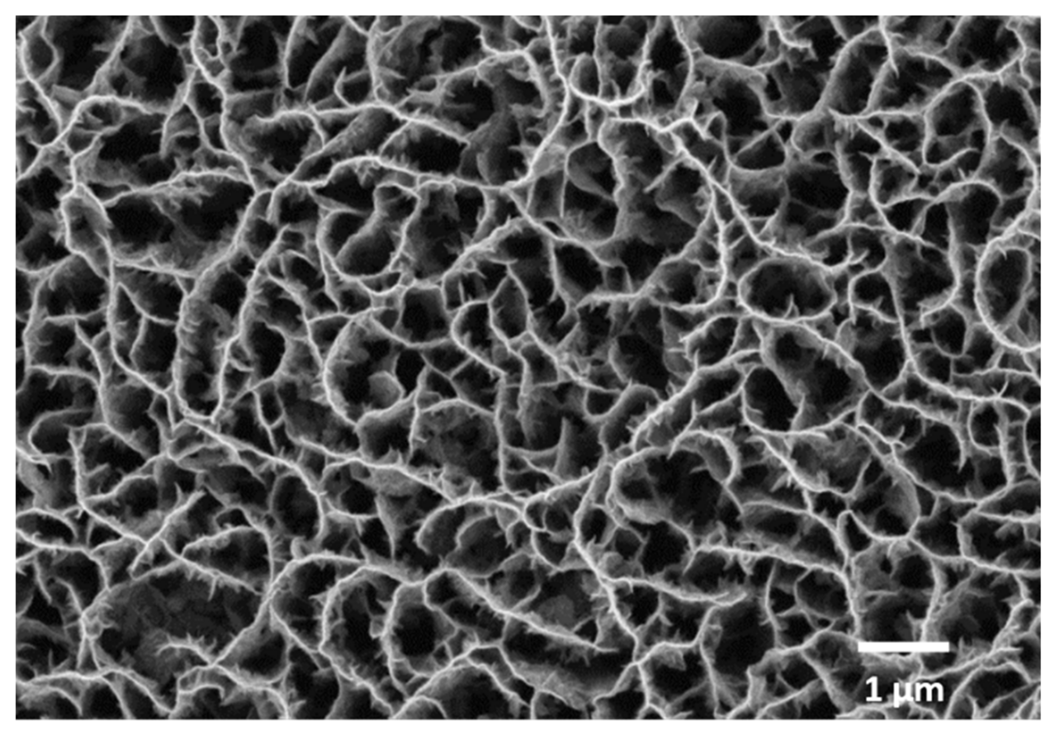
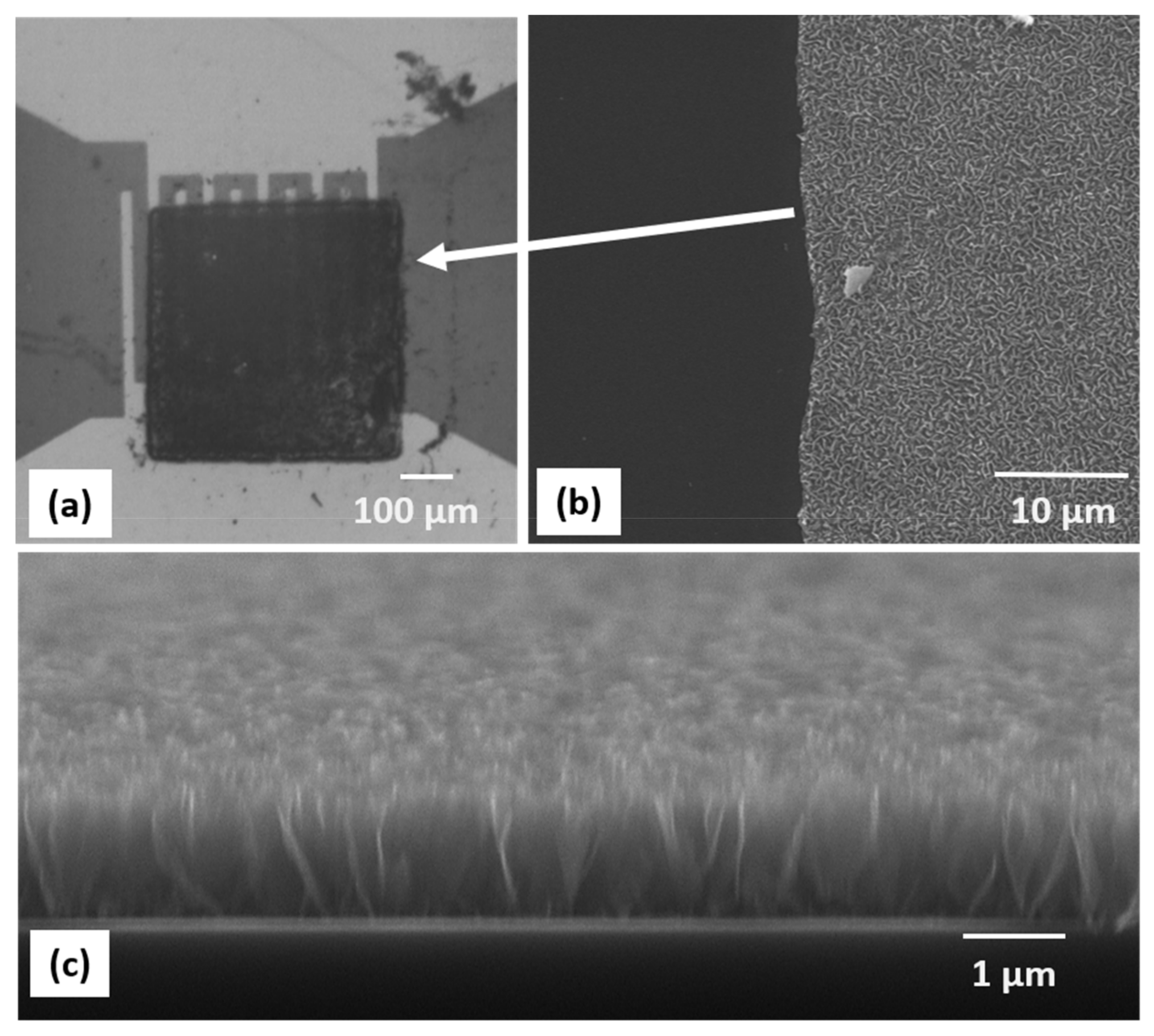
2.1. Fabrication of CNWs
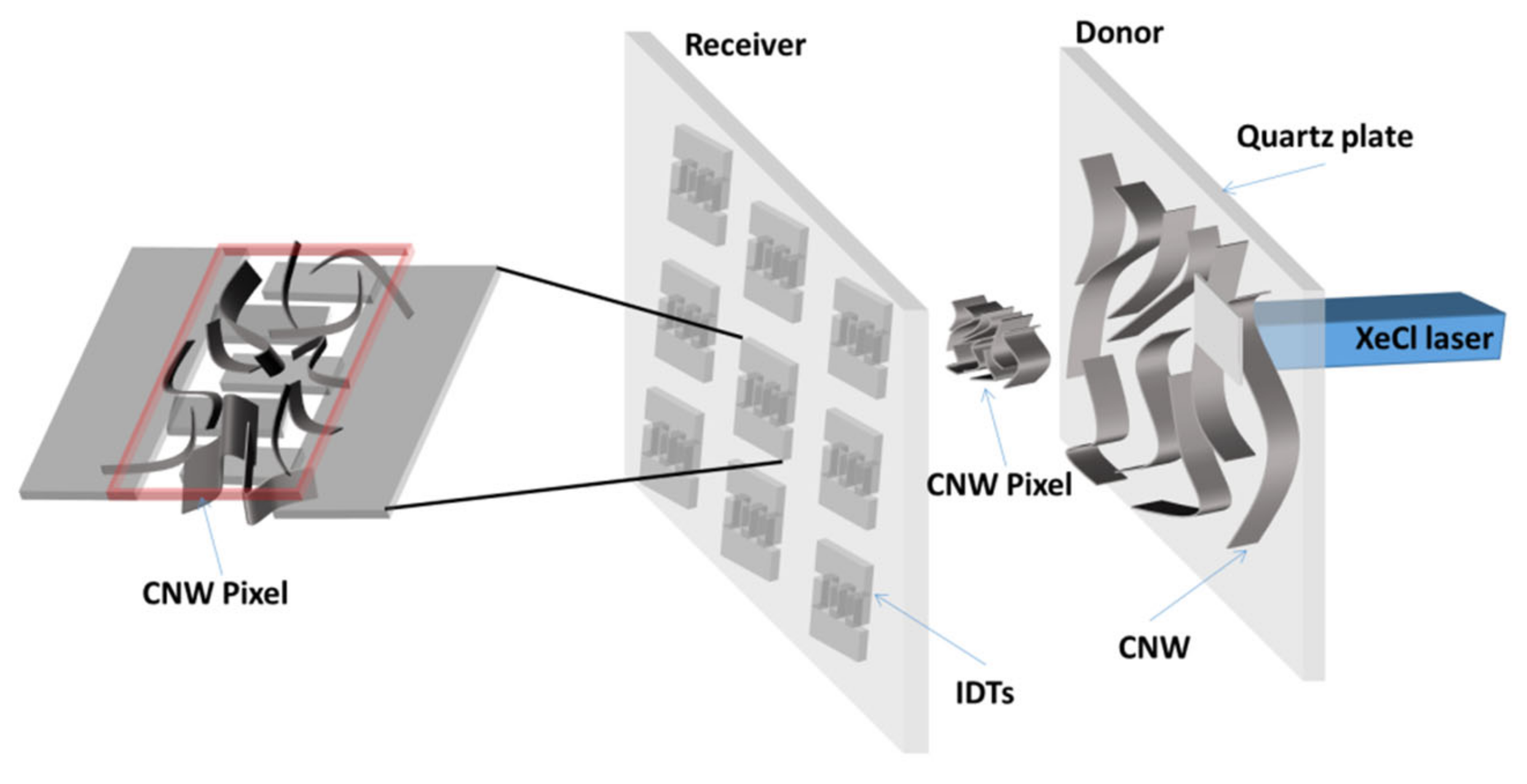
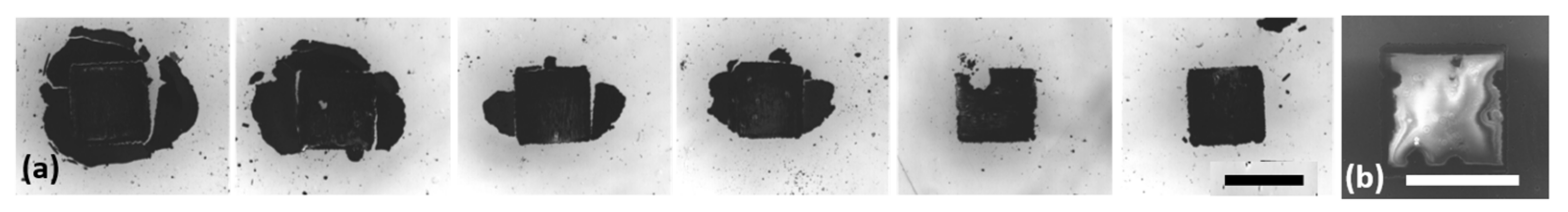
2.2. LIFT Setup
2.3. Sensor Tests
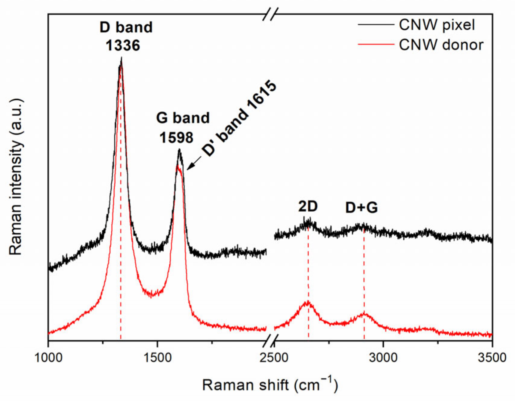
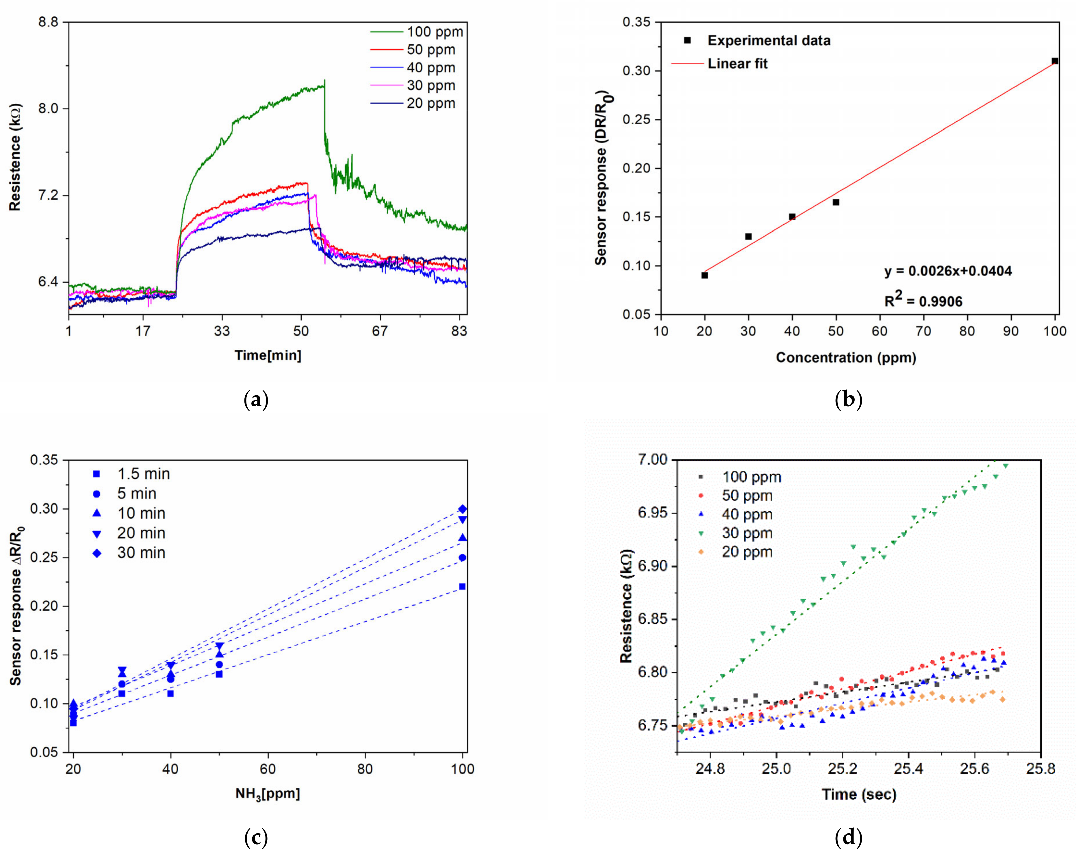
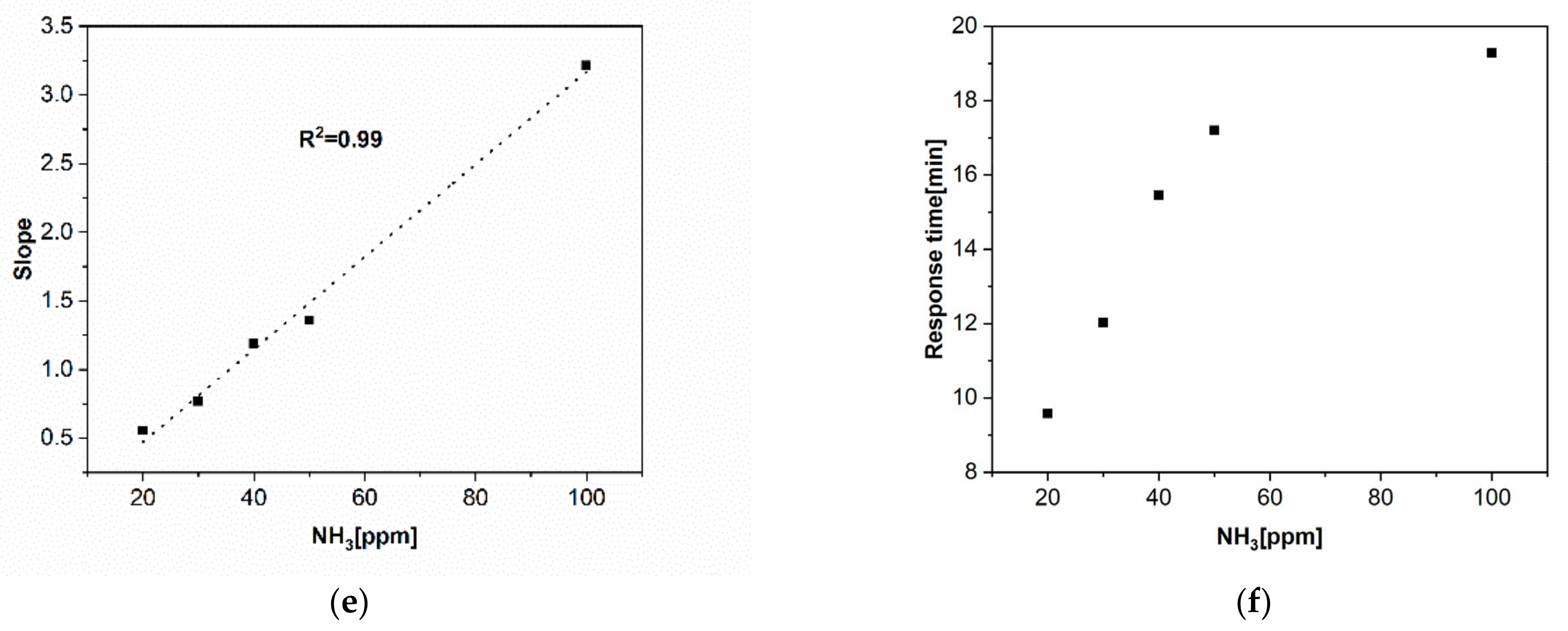
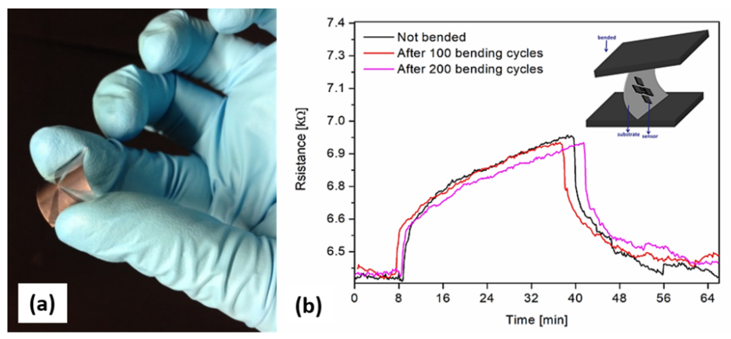
3. Results
4. Conclusions
Supplementary Materials
Author Contributions
Funding
Institutional Review Board Statement
Informed Consent Statement
Data Availability Statement
Conflicts of Interest
References
- Lu, J.G. Air Pollution: A Systematic Review of Its Psychological, Economic, and Social Effects. Curr. Opin. Psychol. 2020, 32, 52–65. [Google Scholar] [CrossRef]
- Fan, Y.; Zhu, X.; Sui, H.; Sun, H.; Wang, Z. Design and Application of Toxic and Harmful Gas Monitoring System in Fire Fighting. Sensors 2019, 19, 369. [Google Scholar] [CrossRef]
- Jiang, B.; Dehong, X. Role identification of NH3 in atmospheric secondary new particle formation in haze occurrence of China. Atmos. Environ. 2017, 163, 107–117. [Google Scholar] [CrossRef]
- Sommer, S.G.; Webb, J.; Hutchings, N.D. New Emission Factors for Calculation of Ammonia Volatilization from European Livestock Manure Management Systems. Front. Sustain. Food Syst. 2019, 3, 101. [Google Scholar] [CrossRef]
- Dey, A. Semiconductor metal oxide gas sensors: A review. J. Mater. Sci. Eng. B 2018, 229, 206–217. [Google Scholar] [CrossRef]
- Palla-Papavlu, A.; Filipescu, M.; Schneider, C.; Antohe, S.; Ossi, P.; Radnóczi, G.; Dinescu, M.; Wokaun, A.; Lippert, T. Direct laser deposition of nanostructured tungsten oxide for sensing applications. J. Phys. D Appl. Phys. 2016, 49, 205101. [Google Scholar] [CrossRef]
- Palla-Papavlu, A.; Mattle, T.; Temmel, S.; Lehmann, U.; Hintennach, A.; Grisel, A.; Wokaun, A.; Lippert, T. Highly sensitive SnO2 sensor via reactive laser-induced transfer. Sci. Rep. 2016, 6, 25144. [Google Scholar] [CrossRef] [PubMed]
- Hu, C.; Song, L.; Zhang, Z.; Chen, N.; Feng, Z.; Qu, L. Tailored graphene systems for unconventional applications in energy conversion and storage devices. Energy Environ. Sci. 2015, 8, 31. [Google Scholar] [CrossRef]
- Hiramatsu, M.; Hori, M. (Eds.) Carbon Nanowalls: Synthesis and Emerging Applications; Springer: Vienna, Austria, 2010. [Google Scholar] [CrossRef]
- Seo, D.H.; Kumar, S.; Ostrikov, K. Control of morphology and electrical properties of self-organized graphenes in a plasma. Carbon 2011, 49, 4331–4339. [Google Scholar] [CrossRef]
- Dinh, T.M.; Achour, A.; Vizireanu, S.; Dinescu, G.; Nistor, L.; Armstrong, K.; Guay, D.; Pech, D. Hydrous RuO2/carbon nanowalls hierarchical structures for all-solid-state ultrahigh-energy-density micro-supercapacitors. Nano Energy 2014, 10, 288–294. [Google Scholar] [CrossRef]
- Shin, J.-H.; Choi, Y.-S.; Park, H.-J. Remote Plasma-Induced Synthesis of Self-Assembled MoS2/Carbon Nanowall Nanocomposites and Their Application as High-Performance Active Materials for Supercapacitors. Nanomaterials 2022, 12, 1338. [Google Scholar] [CrossRef] [PubMed]
- Ghoniem, E.; Mori, S.; Abdel-Moniem, A. An efficient strategy for transferring carbon nanowalls film to flexible substrate for supercapacitor application. J. Power Sources 2021, 493, 229684. [Google Scholar] [CrossRef]
- Yu, K.; Bo, Z.; Lu, G.; Mao, S.; Cui, S.; Zhu, Y.; Chen, X.; Ruoff, R.S.; Chen, J. Growth of carbon nanowalls at atmospheric pressure for one-step gas sensor fabrication. Nanoscale Res. Lett. 2011, 6, X1–X9. [Google Scholar] [CrossRef]
- Zhang, J.; Song, L.; Zhang, Z.; Chen, N.; Qu, L. Environmentally Responsive Graphene Systems. Small 2014, 10, 2151–2164. [Google Scholar] [CrossRef] [PubMed]
- Slobodian, P.; Cvelbar, U.; Riha, P.; Olejnik, R.; Matyas, J.; Filipič, G.; Watanabe, H.; Tajima, S.; Kondo, H.; Sekine, M.; et al. High sensitivity of a carbon nanowall-based sensor for detection of organic vapours. RSC Adv. 2015, 5, 90515–90520. [Google Scholar] [CrossRef]
- Choi, H.; Kwon, S.H.; Kang, H.; Kim, J.H.; Choi, W. Zinc-oxide-deposited Carbon Nanowalls for Acetone Sensing. Thin Solid Film. 2020, 700, 137887. [Google Scholar] [CrossRef]
- Roy, P.K.; Haider, G.; Chou, T.-C.; Chen, K.-H.; Chen, L.-C.; Chen, Y.-F.; Liang, C.-T. Ultrasensitive gas sensors based on vertical graphene nanowalls/SiC/Si heterostructure. ACS Sens. 2019, 4, 406–412. [Google Scholar] [CrossRef] [PubMed]
- Kwon, S.; Choi, H.; Lee, S.; Lee, G.; Kim, Y.; Choi, W.; Kang, H. Room Temperature Gas Sensor Application of Carbon Nanowalls using Electrical Resistance Change by Surface Adsorption of Toxic Gases. Mater. Res. Bull. 2021, 141, 111377. [Google Scholar] [CrossRef]
- Cui, S.; Guo, X.; Ren, R.; Zhou, R.; Chen, J. Decoration of vertical graphene with aerosol nanoparticles for gas sensing. J. Phys. D: Appl. Phys. 2015, 48, 314008. [Google Scholar] [CrossRef]
- Li, J.; Liu, Z.; Guo, Q.; Yang, S.; Xu, A.; Wang, Z.; Wang, G.; Wang, Y.; Chen, D.; Ding, G. Controllable Growth of Vertically-oriented Graphene for High Sensitivity Gas Detection. J. Mater. Chem. C 2019, 7, 5995–6003. [Google Scholar] [CrossRef]
- Bo, Z.; Yuan, M.; Mao, S.; Chen, X.; Yan, J.; Cen, K. Decoration of vertical graphene with tin dioxide nanoparticles for highly sensitive room temperature formaldehyde sensing. Sens. Actuator B Chem. 2017, 256, 1011–1020. [Google Scholar] [CrossRef]
- Chen, G.; Paronyan, T.M.; Pigos, E.M.; Harutyunyan, A.R. Enhanced gas sensing in pristine carbon nanotubes under continuous ultraviolet light illumination. Sci. Rep. 2012, 2, 343. [Google Scholar] [CrossRef] [PubMed]
- Serra, P.; Piqué, A. Introduction to Laser-Induced Transfer and Other Associated Processes. In Laser Printing of Functional Materials: Fundamentals & Applications in Electronics, 3D Microfabrication and Biomedicine; John Wiley & Sons, Ltd.: Hoboken, NJ, USA, 2018; pp. 3–16. ISBN 978-3-527-80510-5. [Google Scholar]
- Delaporte, P.; Alloncle, A.-P. Laser-induced forward transfer: A high resolution additive manufacturing technology. Opt. Laser Technol. 2016, 78, 33–41. [Google Scholar] [CrossRef]
- Visser, C.W.; Pohl, R.; Sun, C.; Roemer, G.-W.; in ’t Veld, B.H.; Lohse, D. Toward 3D Printing of Pure Metals by Laser-Induced Forward Transfer. Adv. Mater. 2015, 27, 4087–4092. [Google Scholar] [CrossRef] [PubMed]
- Gorodesky, N.; Sedghani-Cohen, S.; Fogel, O.; Silber, A.; Tkachev, M.; Kotler, Z.; Zalevsky, Z. Improving Compactness of 3D Metallic Microstructures Printed by Laser-Induced Forward Transfer. Crystals 2021, 11, 291. [Google Scholar] [CrossRef]
- Serra, P.; Duocastella, M.; Fernández-Pradas, J.M.; Morenza, J.L. Liquids microprinting through laser-induced forward transfer. Appl. Surf. Sci. 2009, 255, 5342–5345. [Google Scholar] [CrossRef]
- Papazoglou, S.; Zergioti, I. Laser Induced Forward Transfer (LIFT) of Nano-Micro Patterns for Sensor Applications. Microelectron. Eng. 2017, 182, 25–34. [Google Scholar] [CrossRef]
- Shaw Stewart, J.; Lippert, T.; Nagel, M.; Nüesch, F.; Wokaun, A. Red-Green-Blue Polymer Light-Emitting Diode Pixels Printed by Optimized Laser-Induced Forward Transfer. Appl. Phys. Lett. 2012, 100, 203303. [Google Scholar] [CrossRef]
- Palla-Papavlu, A.; Dinescu, M.; Wokaun, A.; Lippert, T. Laser-Induced Forward Transfer of Single-Walled Carbon Nanotubes. Appl. Phys. A-Mater. Sci. Process. 2014, 117, 371–376. [Google Scholar] [CrossRef]
- Palla-Papavlu, A.; Filipescu, M.; Vizireanu, S.; Vogt, L.; Antohe, S.; Dinescu, M.; Wokaun, A.; Lippert, T. Laser-induced forward transfer of hybrid carbon nanostructures. Appl. Surf. Sci. 2016, 374, 312–317. [Google Scholar] [CrossRef]
- Vizireanu, S.; Stoica, S.D.; Luculescu, C.; Nistor, L.C.; Mitu, B.; Dinescu, G. Plasma techniques for nanostructured carbon materials synthesis. A case study: Carbon nanowall growth by low pressure expanding RF plasma. Sci. Technol. 2010, 19, 034016. [Google Scholar] [CrossRef]
- Gonzalez, Z.; Vizireanu, S.; Dinescu, G.; Blanco, C.; Santamaria, R. Carbon Nanowalls thin films as nanostructured electrode materials in Vanadium Redox Flow Batteries. Nano Energy 2012, 1, 833–839. [Google Scholar] [CrossRef]
- Cancado, L.G.; Takai, K.; Enoki, T.; Endo, M.; Kim, Y.A.; Mizusaki, H.; Jorio, A.; Coelho, L.N.; Magalhaes-paniago, R.; Pimenta, M.A. General equation for the determination of the crystallite size La of nanographite by Raman spectroscopy. Appl. Phys. Lett. 2006, 88, 163106–216310. [Google Scholar] [CrossRef]
- Constantinescu, C.; Vizireanu, S.; Ion, V.; Aldica, G.; Stoica, S.D.; Lazea-Stoyanova, A.; Alloncle, A.-P.; Delaporte, P.; Dinescu, G. Laser-induced forward transfer of carbon nanowalls for soft electrodes fabrication. Appl. Surf. Sci. 2016, 374, 49–55. [Google Scholar] [CrossRef]
- Bonciu, A.F.; Filipescu, M.; Voicu, S.I.; Lippert, T.; Palla-Papavlu, A. Facile Fabrication of Hybrid Carbon Nanotube Sensors by Laser Direct Transfer. Nanomaterials 2021, 11, 2604. [Google Scholar] [CrossRef] [PubMed]
- Fennell, J.; Hamaguchi, H.; Yoon, B.; Swager, T. Chemiresistor Devices for Chemical Warfare Agent Detection Based on Polymer Wrapped Single-Walled Carbon Nanotubes. Sensors 2017, 17, 982. [Google Scholar] [CrossRef] [PubMed]
- Yu, K.; Wang, P.; Lu, G.; Chen, K.-H.; Bo, Z.; Chen, J. Patterning Vertically Oriented Graphene Sheets for Nanodevice Applications. J. Phys. Chem. Lett. 2011, 2, 537–542. [Google Scholar] [CrossRef]
- Meng, Z.; Aykanat, A.; Mirica, K.A. Welding Metallophthalocyanines into Bimetallic Molecular Meshes for Ultrasensitive, Low-Power Chemiresistive Detection of Gases. J. Am. Chem. Soc. 2019, 141, 2046–2053. [Google Scholar] [CrossRef]
- Tan, T.C.; Li, F.; Neoh, K.G. Measurement of BOD by Initial Rate of Response of a Microbial Sensor. Sens. Actuator B Chem. 1993, 10, 137. [Google Scholar] [CrossRef]
- Bohrer, F.I.; Sharoni, A.; Colesniuc, C.; Park, J.; Schuller, I.K.; Kummel, A.C.; Trogler, W.C. Gas Sensing Mechanism in Chemiresistive Cobalt and Metal-Free Phthalocyanine Thin Films. J. Am. Chem. Soc. 2007, 129, 5640. [Google Scholar] [CrossRef]


| Material | Analyte | Concentration (ppm) | Sensor Performance | Ref. |
|---|---|---|---|---|
| Epitaxial graphene nanowalls | H2 | 0.5–500 | LOD 0.5 ppm | [18] |
| 500 ms response time | ||||
| CNWs | NH3 | 1% in air | NA * | [14] |
| NO2 | 100 ppm | NA | ||
| CNWs | NH3 | 1% in air | NA | [39] |
| NO2 | 100 ppm | NA | ||
| CNWs | NH3 NO2 | 25–100 25–100 | LOD 15 ppm LOD 20 ppm | [19] |
| CNWs with 100 and 300 nm interwall distance | Acetone | NA | Response time of (100 nm) 65.4 (300 nm) and 8.5 | [16] |
| Methanol Diethyl ether Iso–pentane | NA NA NA | (100 nm) 327.1 and (300 nm) 36.2 (100 nm) 273.8 and (300 nm) 34.1 (100 nm) 87.2 and (300 nm) 46.6 | ||
| Vertical graphene nano–petals | NH3 | 10–100 ppt | Joule heating to 100 °C is used during desorption | [21] |
Publisher’s Note: MDPI stays neutral with regard to jurisdictional claims in published maps and institutional affiliations. |
© 2022 by the authors. Licensee MDPI, Basel, Switzerland. This article is an open access article distributed under the terms and conditions of the Creative Commons Attribution (CC BY) license (https://creativecommons.org/licenses/by/4.0/).
Share and Cite
Palla-Papavlu, A.; Vizireanu, S.; Filipescu, M.; Lippert, T. High-Sensitivity Ammonia Sensors with Carbon Nanowall Active Material via Laser-Induced Transfer. Nanomaterials 2022, 12, 2830. https://doi.org/10.3390/nano12162830
Palla-Papavlu A, Vizireanu S, Filipescu M, Lippert T. High-Sensitivity Ammonia Sensors with Carbon Nanowall Active Material via Laser-Induced Transfer. Nanomaterials. 2022; 12(16):2830. https://doi.org/10.3390/nano12162830
Chicago/Turabian StylePalla-Papavlu, Alexandra, Sorin Vizireanu, Mihaela Filipescu, and Thomas Lippert. 2022. "High-Sensitivity Ammonia Sensors with Carbon Nanowall Active Material via Laser-Induced Transfer" Nanomaterials 12, no. 16: 2830. https://doi.org/10.3390/nano12162830
APA StylePalla-Papavlu, A., Vizireanu, S., Filipescu, M., & Lippert, T. (2022). High-Sensitivity Ammonia Sensors with Carbon Nanowall Active Material via Laser-Induced Transfer. Nanomaterials, 12(16), 2830. https://doi.org/10.3390/nano12162830