Article

Cuγ (γ = 1–3)-Modified MoS2 Monolayer as a Gas Sensor for Detecting C4F7N and Its Decomposition Components

1
College of Electrical Engineering and Automation, Shandong University of Science and Technology, Qingdao 266590, China
2
Department of Electrical Engineering, Tsinghua University, Beijing 100084, China
*
Author to whom correspondence should be addressed.
Nanomaterials 2022, 12(16), 2829; https://doi.org/10.3390/nano12162829
Submission received: 11 July 2022 / Revised: 26 July 2022 / Accepted: 13 August 2022 / Published: 17 August 2022
(This article belongs to the Section Synthesis, Interfaces and Nanostructures)

Abstract

:
Perfluorinated isobutyronitrile (C4F7N) is favored in electrical engineering because it is an environmentally friendly gas-insulating medium with a low greenhouse effect. Unfortunately, under the influence of electricity and over-heating, its decomposition results in the deterioration of its insulating properties, which potentially leads to partial discharge or even gas breakdown. In this paper, the adsorption behavior of C4F7N gas and its toxic decomposition product, acetonitrile (C2N2), on MoS2 surfaces doped with small copper clusters was investigated by calculating the adsorption energy and density of states, etc. The effects of multiple initial adsorption positions as well as externally applied electric fields were also taken into account. The results depict that the maximum adsorption energy of C4F7N on the Cuγ (γ = 1–3)-MoS2 surface gradually decreases with the increase in γ. The Cu3-modified MoS2 is most suitable for use as a resistive-based gas-sensitive sensor substrate. This paper provides the theoretical foundation for the maintenance of future power equipment with environmentally friendly insulating gas.

1. Introduction

Sulfur hexafluoride (SF6) gas, due to its excellent insulating properties such as its high dielectric strength and arc quenching performance, is mostly and widely used in Gas-insulated Switchgear (GIS), Gas-insulated Line (GIL), Gas-insulated Cabinet (GIC) and other gas-insulated power equipment in electric power transmission and distribution projects. However, SF6 is a powerful greenhouse gas with about 23,500 times the global warming potential (GWP) of that of CO2 [1]. The green development of global electrical engineering is an inevitable requirement in sake of environmental protection, which required that the use of SF6 must be reduced. To meet both the high dielectric strength and environmental protection demands, C4F7N, with a GWP of 2090 and a dielectric strength two times higher than that of SF6, was found by the 3M company in 2019. The first GIC using C4F7N gas was developed by the China Institute of Electrical Technology in the same year.
However, in the operating of electrical equipment, C4F7N is subjected to electrical and thermal stresses, resulting in the degradation of the insulating gas. By monitoring the composition and content of the pyrolysis product, the insulating property of C4F7N can be characterized. Hence, to ensure the safe and stable operation of C4F7N gas-insulated electric power equipment, it is necessary to detect the decomposition products of C4F7N in real time so as to diagnose early insulation faults. To achieve this goal, it is necessary to clarify the byproduct components of C4F7N and master the fundamental detection principle of each component.
G.Q. Zhang et al. investigated the partial discharge (PD) decomposition characteristics of C4F7N mixed with CO2 with a pin-plate discharge test model, and the results showed that the pyrolysis components of C4F7N mainly contained C2F6, C2F4, C3F6, CF3CN and C2N2 [2]. X. Zhang et al. conducted a 96 h PD decomposition test on C4F7N/CO2 gas mixtures using a needle-plate electrode and clarified that the characteristic decomposition components include CO, CF4, C2F6, CF3CN, C2N2 and COF2 [3]. Further, they showed that the contents of CO, CF4, C2F6, CF3CN and C2N2 were significantly higher than those of other components. In 2017, B. Radisavljevic et al. investigated the decomposition characteristics of 9.5% C4F7N-9.5% O2-81% CO2 gas mixtures under arc discharge conditions and found that the decomposition of C4F7N mainly incorporated CO, CF4, C2F4, CF3CN, C2F5CN and C2N2 [4]. Furthermore, the particles produced by the decomposition of C4F7N under arc discharge conditions were not recoverable. Q.D. Huang et al. studied the overheated decomposition properties of a C4F7N/CO2/O2 gas mixture and found that its main decomposition product also contained C2N2 gas [5]. These results suggest that C2N2 can be used as a characteristic component of C4F7N decomposition that reacts to the aging state of C4F7N insulation under electrical and thermal faults.
C2N2 is highly toxic and readily reduced to cyanide. A. Beroual and C. Preve assessed the occupational exposure limit of 10 μL/L (8 h) with an inhalation test in rats and observed that the prolonged inhalation of C2N2 caused a break in the mitochondrial transfer chain of the rat cells and caused respiratory and visual irritation [6,7]. Meanwhile, it revealed that a break in the mitochondrial transfer chain of the rat cells and a strong irritation of the respiratory and visual systems, which could lead to health hazards and even death, was caused by the prolonged inhalation of C2N2. Therefore, it is particularly important to ensure the safety of the operation and the maintenance of the electrical equipment using C4F7N as the insulating medium.
MoS2, as a new semiconductor gas-sensitive material with a high surface area ratio and a natural semiconductor band gap [8], is broadly used in semiconductor-based micro gas-sensitive sensors as well as in the fabrication of adsorbents. However, the gas sensitivity of intrinsic MoS2 for specific gases is often unsatisfactory, and transition metal catalyst doping is used for gas sensitivity [9,10]. Cuprum (Cu) is a relatively inexpensive transition metal catalyst compared to precious metal catalysts such as aurum (Au), argentum (Ag) and platinum (Pt). Existing studies on the gas sensitivity of Cu and its cognate elements doped with MoS2 for specific gases demonstrate that Cu can be an excellent candidate for the MoS2 doping of two-dimensional materials. For example, the enhancement of the gas sensitivity of C2H2 by Au- and Ag-doped MoS2 was studied, and the results indicated that the doping of Au and Ag in the same main group can improve the gas sensitivity of dissolved gas C2H2 in insulating oil [11,12]. Furthermore, the gas sensitivity of pure and Cu-doped MoS2 to CO and NO was discussed in document [13]. It was found that Cu doped with sulfur (S) site can significantly improve the adsorption energy for CO and NO. Furthermore, according to the Hund’s rule of external electron configuration and the external electron configuration law, the external electron configuration formula of Cu is [Ar] 3d104s1. As far as transition metal elements are concerned, the outermost electron number of Cu is 1, which will make Cu atoms easily bond with the lone pair electrons of C, N and F atoms in the decomposition products of C4F7N, forming a strong adsorption force and achieving the purpose of capturing specific gases by gas-sensitive materials. It can be concluded that Cu may be the most ideal doping element to improve the gas sensitivity of MoS2 to C4F7N and its decomposition products.
The manuscript is structured as follows: First, the DMol3 module in Materials Studio software is used to model and calculate the stable structure of Cu cluster-modified MoS2. Second, the electronic density of states and the charge transfer amounts before and after the adsorption of C4F7N and C2N2 are compared to obtain the gas-sensitive mechanism of Cu-modified MoS2 for the detection of C4F7N and its decomposition products. Third, the gas-sensitive performance of the optimal doping system under different electric fields is investigated considering the complex working conditions of power equipment. This paper investigates the adsorption mechanism of the environmentally friendly insulating gas C4F7N and its decomposition product C2N2 on the Cu cluster-modified MoS2 surface through theoretical calculations and lays the groundwork for the gas content monitoring of the new electrical insulation equipment using C4F7N2.
The structure and energy optimization of the computational model was carried out based on the first principles of Density Functional Theory (DFT). We first constructed a 4 × 4 × 1 MoS2 supercell structure. Since it is necessary to find a section for quantum mechanical adsorption calculation, the (0,0,1) section was selected in this work, and a vacuum layer with a thickness of 15 Å was established to prevent reactions between different periods. Then, the PBE function based on DFT and the GGA of the spin polarization measurement were selected to deal with the calculation problem of electron crosslinking [14]. The molecular structures of C4F7N, C2N2 and Cu clusters were optimized, and the optimal structures are shown in Figure 1. Detailed bond lengths and bond angles of C4F7N, C2N2 and Cu cluster molecules are shown in Table 1.
The DFT-D2 method was used for dispersion correction [15], and the energy threshold, convergence force and self-consistent field were set as 1 × 10⁻⁵ Ha (1 Ha = 27.2114 eV), 2 × 10⁻³ Ha/Å and 1 × 10⁻⁶ eV, respectively, with a maximum displacement of 0.005 Å [16]. Since the formation of molecular orbits deforms atomic orbits to some extent, resulting in the deviation between the calculated results and the actual situation, double numerical polarization (DNP) was adopted to calculate the exchange electron pseudopotential to obtain more accurate results [17]. In orbital electronic processing, a single effective potential (DFT semicore Pseudopots (DSPP)) was used to replace the core electron to reduce the computational cost [18]. In the model surface calculation, the k point in the Brillouin region was set as 5 × 5 × 1 [13].
The stability of doped structures can be measured by binding energy (Eb) [14], and it can be determined by Equation (1), as follows:
E b = E ( Cu ) γ - MoS 2 ( E MoS 2 + E ( Cu ) γ )
where E(Cu)γ-MoS2, EMoS2 and E(Cu)γ represent the binding energies of (Cu)γ-MoS2, pure MoS2 and the Cu cluster, respectively.
The adsorption energy (Eads) can be calculated by Equation (2), which is as follows:
E ads = E ( substrate + gas E substrate E gas )
where Esubstrate+gas represents the total energy of the gas molecule adsorbed on the Cuγ-MoS2 surface, Esubstrate and Egas are the energies of Cuγ-MoS2 and a gas molecule, respectively.
The charge amount is obtained by Mullikan [12] charge analysis. The transferred charge (Qt) is determined by Equation (3), which is as follows:
Q t = Q ads Q iso
where Qads and Qiso represent the total charge of gases after and before adsorption, respectively.

2. Results and Discussion

The adsorption energy Eads proves whether the reaction can be spontaneous and indicates the strength of the adsorption reaction [19]. If Eads < 0, the reaction releases energy, indicating that the adsorption reaction can be spontaneous. The transferred charge quantity Qt can be used to explain the charge exchange level between the gas molecule and the substrate and then to explain the change in the conductivity of the system.

2.1. Construction of Stable Structures of Cu Clusters-Doped MoS2

The most stable modified structure obtained by calculating the binding energy of Cu clusters doped at different positions, such as Sulfur (S), Molybdenum (Mo) and bridge positions according to Equation (1), is shown in Figure 2. The yellow atom in the diagram is S, and the cyan atom is Mo. The binding energies of the Cu clusters with MoS2 are calculated from Equation (1) to be −1.723, −1.831 and −2.976 eV, respectively, all of which are greater than −0.6 eV [19], indicating that the structure has strong stability. Three S-Cu bonds with bond lengths of 2.261, 2.263 and 2.262 Å and a Mo-Cu bond of 2.876 Å are formed on the MoS2 surface by single Cu atoms. Meanwhile, four S-Cu bonds with lengths of 2.302, 2.333, 2.343 and 2.322 Å are formed between Cu2 and the S atoms of MoS2. Interestingly, the bond length of Cu2 increased significantly from 2.253 Å before modification to 2.380 Å, indicating that Cu-Cu is activated, which is strong evidence of its stability in binding to MoS2. Similarly, Cu3 breaks a Cu-Cu bond upon binding to MoS2, forming six S-Cu bonds with bond lengths of 2.303, 2.360, 2.323, 2.326, 2.308 and 2.357 Å, respectively. Further, the electronic density of states (DOS) and partial density of states (PDOS) distributions for (Cu)γ-MoS2 and pure MoS2 are obtained, which are shown in Figure 3.
As shown in Figure 3, the electron density distribution of MoS2 changes significantly after the Cuγ (γ = 1, 2, 3) modification, which is reflected in the significant leftward shift of the DOS diagram compared to the intrinsic MoS2, resulting in a decrease in the electron energy level. Based on the PDOS diagram of Cu-MoS2 in Figure 3, it can be seen that the electron densities of Cu-3d and S-3p peak simultaneously and are close to −6, −4 and −2 eV, indicating that strong orbital hybridization between the two has been formed. The two orbit peaks of S-3p and Mo-4d at 2 eV overlap. The aforementioned facts reasonably explain the bond forming between the Cu and S atoms in Cu-MoS2.
As far as the Cu2-MoS2 system is concerned, the electron density increases near the Fermi level (E = 0 eV), which indicates that there is an increase in conductivity for the Cu2-modified system. In terms of electron orbit analysis, the Cu-3d, Mo-4d and S-3p orbits have strong orbital hybridization around −1.5 eV. The electron density contribution from the Cu-4s orbit is responsible for the elevated electron density near the Fermi level. The PDOS diagram of the Cu3-MoS2 system shows that the Cu-3d, Mo-4d and S-3p orbits reach a simultaneous maximum in electron density at −3.5 eV, which accounts for the bonding of Cu to S atoms.

2.2. Adsorption on the Cu-MoS2 Monolayer

Figure 4 shows the four different conformations of C4F7N and C2N2 adsorbed on the Cu-MoS2 surface, and the candidates are labeled as X11, X12, X21 and X22, respectively. The magnitudes of the adsorption energies of the four systems calculated with Equation (2) are as follows: Eads(X21) = −1.080 eV > Eads(X11) = −1.011 eV > Eads(X22) = −0.632 eV > Eads(X12) = −0.235 eV. According to the calculated adsorption energy, the adsorption strength of the Cu-MoS2 system is slightly greater than that of C4F7N for C2N2, and both of them are spontaneous adsorption. Here, only X11 and X21, which have larger adsorption energies, are taken as examples for further analysis. The minimum adsorption distance between C4F7N and C2N2 on the Cu-MoS2 surface is 1.856 Å, and the electron density distribution after adsorption is shifted to the left, as shown in Figure 4 and Figure 5a. The electron difference density (EDD) plots for X11 and X21 are shown in Figure 5b,c, where the red region indicates electron loss and the blue region indicates electron enrichment. The C and N atoms of CN* of C4F7N in X11 are surrounded by the red region, indicating electron loss, and the Cu atoms are surrounded by the blue electron cloud, indicating electron gain by the Cu atom. In contrast, the red region in X21 is distributed around the two CN* of C2N2, which demonstrates an overall loss of electrons and a transfer of electrons to the substrate.
For X11, the C-2p and N-2p orbits near −9.5 and −4 eV have a clear overlap of orbit peaks with the Cu-3d orbit, forming a strong orbital hybridization, as shown by the DOS and PDOS distributions in Figure 5a. The orbital overlap of Cu-3d with N-2p near the Fermi energy level reasonably explains the bonding of the N atom of CN* to the Cu atom in C4F7N. Based on the amount of transferred charge charge of X11 (0.176e), C4F7N is positively charged after adsorption, indicating that it acts as an electron donor transferring electrons to the substrate, which results in an increase in the conductivity of the substrate. Similarly, for the X21 system, the orbital hybridization of C-2p, N-2p and Cu-3d is mainly at −8 and −4.5 eV. Unlike C4F7N, the orbital hybridization of N-2p and Cu-3d after the adsorption of C2N2 on the Cu-MoS2 surface is mainly concentrated near the −5 eV, which is closer to the Fermi energy level, and this is the reason why the surface interaction between C2N2 and Cu-MoS2 is stronger than that of C4F7N. The transferred charge of C2N2 is 0.024e, again acting as an electron donor to the substrate.

2.3. Adsorption on the Cu2-MoS2 Monolayer

The four stable structures of C4F7N and C2N2 adsorbed on the Cu2-MoS2 surface are shown in Figure 6. They are named as X31, X32, X41 and X42, respectively. According to Equation (2), the calculated magnitudes of the adsorption energies are as follows: Eads(X41) = −1.572 eV > Eads(X31) = −0.956 eV > Eads(X42) = −0.6–0.662 eV > Eads(X32) = −0.184 eV. Here, only X41 and X31, which have a higher adsorption energy, are taken for further analysis. Figure 7 shows the DOS and PDOS of X41 and X31 after adsorption. Based on the DOS diagram shown in Figure 7a, the variation in the density of electron states from −2 to −4 eV after the adsorption of C2N2 is more pronounced than that of C4F7N, which reasonably indicates that the adsorption of C2N2 with the Cu2-MoS2 surface is stronger than that of C4F7N. In detail, with the PDOS diagram shown in Figure 7, the X31 structure has orbital hybridization present at −8 and −6 eV for C-2p, N-2p and Cu-3d. The X41 system has orbital hybridization at −6 and −5 eV for C-2p, N-2p and Cu-3d, and it is close to the Fermi energy level. The transferred charge of C2N2 in the X41 system is −0.186e after adsorption by the Cu2-MoS2 surface, which acts as an electron acceptor, and electrons are transferred from the substrate to the C2N2 molecule, resulting in a decrease in the substrate conductivity. The transferred charge (0.134e) and adsorption energy of the system of X31 are both reduced compared to the system of X11. The EDD plots for X31 and X41 are shown in Figure 7b,c. The N atom of the CN* of C4F7N in X31 is surrounded by a red region, indicating electron loss, while the Cu atom is surrounded by a blue electron cloud, indicating electron gain from the Cu atom. The red region in X41 is distributed around the CN* of C2N2, which proves its loss of electrons and the transfer of electrons to the two Cu atoms.

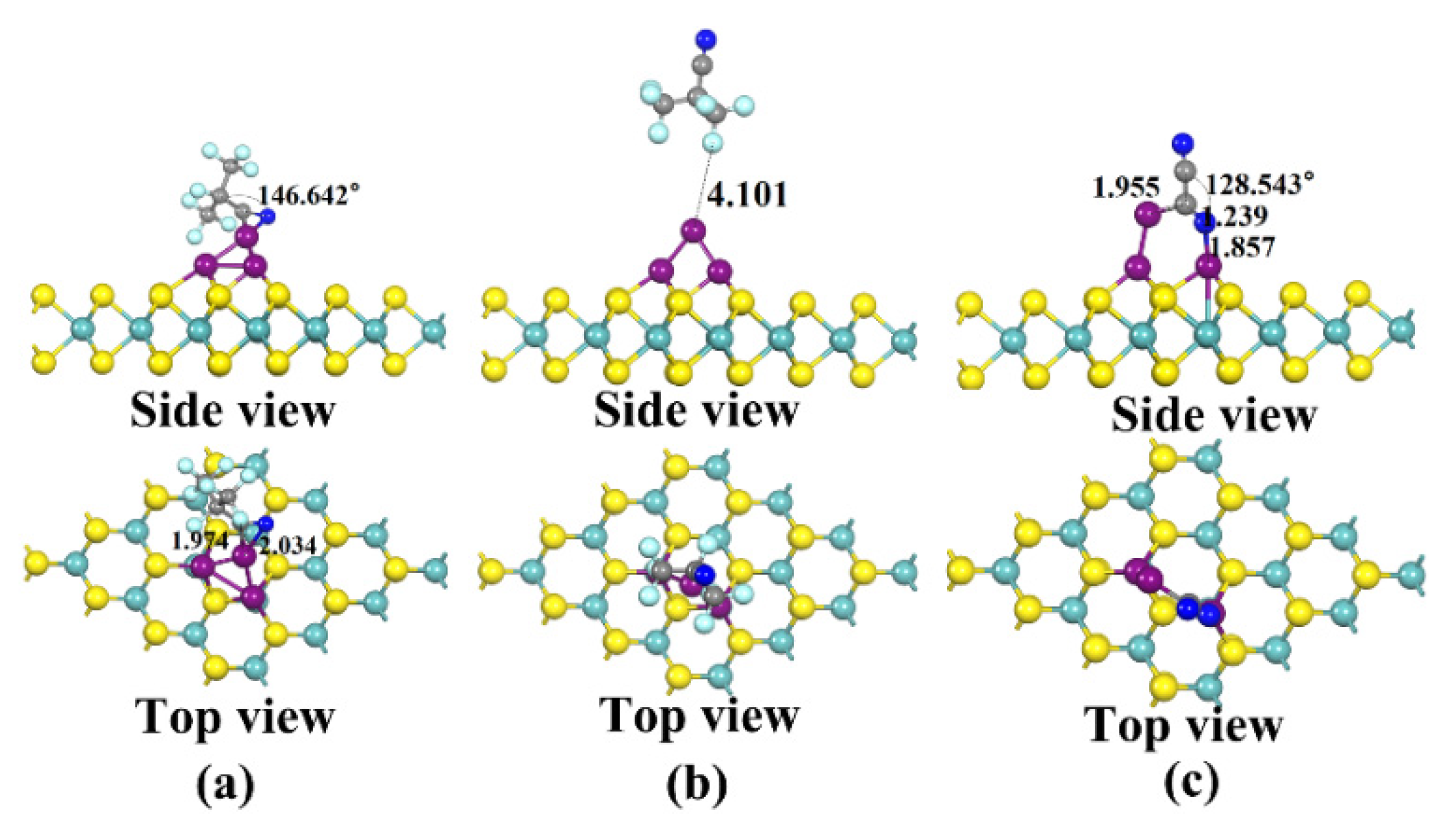
2.4. Adsorption on the Cu3-MoS2 Monolayer

The three stable structures of the two gases adsorbed on the Cu3-MoS2 surface, C4F7N and C2N2, are shown in Figure 8 and are named X51, X52 and X61, respectively. The adsorption energies are listed as follows: Eads(X61) = −1.09 eV > Eads(X51) = −0.770 eV > Eads(X52) = −0.239 eV. For X51, the C4F7N gas molecule undergoes a large change in shape after adsorption. This is demonstrated by the reduction in the bond angle of C-C≡N from 179.697° to 146.642° before adsorption and the shortest distance for adsorption of 1.974 Å. The PDOS diagram, shown in Figure 9a, shows that the C-2p, N-2p and Cu-3d orbital hybridization is mainly concentrated in the −4 to −7.5 eV range. From the calculated adsorption energy magnitude, it is learned that the adsorption energy of the X51 system is less than −0.6 eV, which means that chemisorption can no longer be constituted. In contrast, the degree of change in the structure of X61 after C2N2 adsorption is more pronounced compared to that of X51. In detail, the bond angle of C2N2 of C-C≡N drops sharply from 179.931° before adsorption to 128.543° and forms a “ring” structure with the Cu3 cluster. At the same time, orbital hybridization exists at −5.5 to −7 eV and at −3.5 eV for C-2p, N-2p and Cu-3d. According to the EDD diagram shown in Figure 9b,c, it can be seen that the distribution of the electron cloud around the C4F7N molecule in X51 is not obvious, indicating a relatively small amount of charge transfer. The blue region in X61 is distributed around C in the CN* above C2N2, which proves that it has gained electrons.
From Figure 10, it can be seen that the maximum adsorption energy of Cuγ-MoS2 for C4F7N shows a decreasing trend as the value of the Cu cluster γ (γ = 1, 2, 3) increases. The transferred charge is 0.003e, tending to 0, which has less of an effect on the conductivity of the substrate. At this point, Cuγ-MoS2 can still satisfy the chemisorption for C2N2 with good selectivity. Therefore, Cu3 small clusters modified with MoS2 can avoid main gas interference and be used as a sensitive substrate for the detection of C2N2-resistive gas sensors.

2.5. Externally Applied Electric Field

This is investigated by applying positive and negative polar electric fields perpendicular to the X61 system. The effect of the externally applied electric field on the adsorption energy and charge transfer of X61 is shown in Figure 11. In Figure 11, 1 a.u is equal to 51.36 V/Å. As can be seen from Figure 11, the application of either a positive or negative electric field is detrimental to the adsorption energy, resulting in a reduction in the adsorption energy. However, when a positive polar electric field is applied, the electrons due to the electric field force cause the electrons gained by the C2N2 gas molecules to increase with the increase in the electric field value. In general, although the adsorption energy and the magnitude of the transferred charge are influenced by the applied electric field, they still meet the detection requirements.

2.6. Band Strcture and Recovery Time of C2N2-Cu3/MoS2

We calculated the change in the band gap values before and after the adsorption of C2N2 gas on the Cu3/MoS2 surface are shown in Figure 12. In this case, the Brillouin zone scan path was set to G-M-K-G during the calculation of the bandgap map. The calculated band gap value of the adsorbed C2N2 gas molecules is 1.201 eV, which is 10.5% higher than the band gap value of 1.087 eV of the Cu3-MoS2 system before adsorption, which is consistent with our previous finding that C2N2 acts as an electron acceptor and thus leads to a decrease in the conductivity of the Cu3-MoS2 system. Meanwhile, we calculated from Equation (4) that the desorption time of C2N2 at 370 K is 645 s, which can have good recovery characteristics.
The general formula for calculating the recovery time of a gas-sensitive substrate is defined as [20,21]:
τ = e E ads / K T v 0
where υ0 is the apparent frequency (here, we take 1012 s−1); Eads is the adsorption energy; K is the Boltzmann constant (8.62 × 10⁻⁵ eV/K); T is the temperature (K).

3. Synthesis of Cu Clusters-Doped MoS2 Gas-Sensitive Materials

In this paper, Cu-containing cluster-doped MoS2 gas-sensitive materials were synthesized at the experimental level. The specific synthesis process is shown in Figure 13. The analytical pure grade drugs involved in the synthesis of this paper were purchased from Shanghai Aladdin. For the synthesis of MoS2 nanosheets, 100 mL of thioglycolic acid (HSCH2CO2H, TA) was first placed in a 250 mL volumetric beaker, and sodium molybdate (Na2MoO4) was added to the above beaker in a 1:3 molar ratio with TA, sealed and stirred for 30 min at room temperature using a magnetic stirrer. For the preparation of the Cu-containing powder, 12 g of Cu(NO3)2·3H2O was first dissolved in 100 mL of distilled water and stirred for 15 min before adding potassium hydroxide (KOH) solution dropwise; the solution gradually became darker in color, and after warming and stirring at 60 °C (333 K), the solution turned black and was left to stand for 12 h to obtain a solid-liquid layered solution. The upper layer of the solution was removed with a dropper, and the solid was centrifuged in a centrifuge at 10,000 r/min, put into an oven, dried at 80 °C for 12 h and ground to obtain Cu powder.
For the synthesis of Cu-containing cluster-doped MoS2, the gas-sensitive material was mainly obtained by mixing the abovementioned synthesized Cu-containing powder as well as MoS2 nanosheets in a 1:9 molar ratio into isopropanol (C3H8O), stirring for 8 h using a magnetic stirrer and then drying. The synthesized MoS2 and the microscopic appearance of the Cu-containing cluster-doped MoS2 are shown in Figure 14. The scanning electron microscope (SEM) image in Figure 14 shows that the MoS2 exhibits a sheet-like structure with a smooth surface. In contrast, the doped MoS2 nanosheets have many tiny clusters attached to them, resulting in a Cu-containing cluster-doped MoS2 composite structure.

4. Conclusions

In this paper, the adsorption mechanism of C4F7N and its electrothermal aging decomposition characteristic component C2N2 on Cuγ (γ = 1–3)-MoS2 are investigated based on the DFT theory by calculating the DOS, the PDOS and the adsorption energy. The following conclusions are obtained.
The maximum adsorption energy of a single Cu atom modified with MoS2 is −1.011 and −1.080 eV for C4F7N and C2N2, respectively. Due to the close proximity of the two values, the selectivity requirements for detection may not be met at this point. However, as the number of doped copper atoms increases, the adsorption energy of the doped system for C4F7N gradually decreases, reaching a minimum value of −0.770 eV at γ = 3. In comparison, the magnitude of the adsorption energy of C2N2 is significantly higher than that of C4F7N at −1.09 eV. The calculated band gap value of the C2N2 gas molecules after adsorption increased by 10.5% compared to the Cu3-MoS2 system before adsorption. This indicates that a more significant decrease in conductivity occurred after adsorption. Moreover, the desorption time of C2N2 at 370 K is 645 s, which can have good recovery characteristics. Small clusters of Cu3-modified MoS2 are therefore suitable as detection gas-sensitive substrates for the detection of the toxic gas C2N2.
When an electric field of positive and negative polarity is applied to Cu3-MoS2, the adsorption energy of C2N2 on the surface of Cu3-MoS2 decreases with the increase in the electric field, but it is still greater than −0.6 eV, which still meets the detection requirements. When a negative polarity electric field is applied, Qt increases as the electric field increases due to the force of the electric field. The conclusions of this paper provide theoretical guidance for the selection of gas-sensitive materials for the decomposition products of C4F7N.

Author Contributions

Conceptualization, C.L. (Changyun Li); methodology, P.C.; software, Y.Y.; validation, C.L. (Changyun Li); formal analysis, P.C.; investigation, P.C.; resources, P.C.; data curation, P.C.; writing—original draft preparation, C.L. (Chuanyang Li); writing—review and editing, visualization, P.C.; supervision, C.L. (Changyun Li); project administration, C.L. (Changyun Li); funding acquisition, C.L. (Changyun Li). All authors have read and agreed to the published version of the manuscript.

Funding

Key R & D Program of Shandong Province (2019GGX102049).

Institutional Review Board Statement

Not applicable.

Informed Consent Statement

Not applicable.

Data Availability Statement

The data that support the findings of this study are available from the corresponding author, [C.L. (Changyun Li)], upon reasonable request.

Acknowledgments

The software materials used in this work were provided by the China University of Petroleum (East China).

Conflicts of Interest

The authors declare no conflict of interest.

References

  1. Li, X.W.; Zhao, H.; Murphy, A.B. SF6-alternative gases for application in gas-insulated switchgear. J. Phys. D Appl. Phys. 2018, 51, 153001. [Google Scholar] [CrossRef]
  2. Zhao, M.Y.; Han, D.; Rong, W.Q.; Zhang, G.Q.; Huang, H.; Liu, Z.E. Decomposition Characteristics of Binary Mixtures of (CF3)2CFCN Buffer Gases Under Corona Discharge. High Volt. Eng. 2019, 45, 1078–1085. [Google Scholar]
  3. Li, Y.; Zhang, X.X.; Fu, M.L.; Xiao, S.; Tang, J.; Tian, S.S. Research and Application Progress of Eco-Friendly Gas Insulating Medium C4F7N, Part Ι: Insulation and Electrical, Thermal Decomposition Properties. Trans. China Electrotech. Soc. 2021, 36, 3535–3552. [Google Scholar]
  4. Radisavljevic, B.; Stoller, P.C.; Doiron, C.B. Switching performance of alternative gaseous mixtures in high-voltage circuit breakers. In Proceedings of the International Symposium on High Voltage Engineering, Buenos Aires, Argentina, 28 August–1 September 2017. [Google Scholar]
  5. Huang, Q.D.; Luo, Y.; Song, H.Y.; Fu, M.L.; Wang, W.; Wang, D.B. Experimental Study on Partial Over-thermal Decomposition Characteristics of C4F7N/CO2/O2 Gas Mixture. High Volt. Appar. 2021, 57, 112–119. [Google Scholar]
  6. Beroual, A.; Haddad, A.M. Recent advances in the quest for a new insulation gas with a low impact on the environment to replace sulfur hexafluoride (SF6) gas in high-voltage power network applications. Energies 2017, 10, 1216. [Google Scholar] [CrossRef]
  7. Preve, C.; Maladen, R.; Piccoz, D. Validation method and comparison of SF6 alternative gases. In Proceedings of the 23rd International Conference on Elecricity Distribution, Paris, France, 16–21 June 2016. [Google Scholar]
  8. Dasgupt, U.; Chatterjee, S.; Pal, A.J. Thin-film formation of 2D MoS2 and its application as a hole-transport layer in planar perovskite solar cells. Sol. Energ. Mat. Sol. C 2017, 172, 353–360. [Google Scholar] [CrossRef]
  9. Salih, E.; Ayesh, A.I. First principle study of transition metals doped MoS2 as a gas sensor for the detection of NO and NO2 gases. Phys. E 2021, 131, 114736. [Google Scholar] [CrossRef]
  10. Jiang, T.Y.; He, Q.Q.; Bi, M.Q.; Chen, X.; Sun, H.; Tao, L.Q. First-principles calculations of adsorption sensitivity of Au-doped MoS2 gas sensor to main characteristic gases in oil. J. Mater. Sci. 2021, 56, 13673–13683. [Google Scholar] [CrossRef]
  11. Wang, J.X.; Zhou, Q.; Gui, Y.G.; Chen, W.G. Adsorption of C2H2 from oil by doped Molybdenum sulfide. High Volt. Eng. 2020, 46, 1962–1969. [Google Scholar]
  12. Wang, J.X.; Zhou, Q.; Xu, L.N. Gas sensing mechanism of dissolved gases in transformer oil on Ag–MoS2 monolayer: A DFT study. Phys. E 2020, 118, 113947. [Google Scholar] [CrossRef]
  13. Sharma, A.A.; Khan, M.S.; Husain, M.; Khan, M.S.; Srivastava, A. Sensing of CO and NO on Cu-Doped MoS2 Monolayer-Based Single Electron Transistor: A First Principles Study. IEEE Sens. J. 2018, 18, 2853–2860. [Google Scholar] [CrossRef]
  14. Perdew, J.; Burke, K.; Ernzerhof, M. Generalized gradient approximation made simple. Phys. Rev. Lett. 1998, 77, 3865–3868. [Google Scholar] [CrossRef] [PubMed]
  15. Zhang, X.X.; Huang, R.; Yu, L. Gas sensing analysis properties of Au-graphene to SF6 decomposition products based on a first principles study. Proc. CSEE 2017, 37, 1828–1834. [Google Scholar]
  16. Clementi, E.; Raimondi, D.L. Atomic screening constants from SCF functions. J. Chem. Phys. 1963, 38, 2686–2689. [Google Scholar] [CrossRef]
  17. Zhang, X.X.; Li, Y.L.; Hu, X.X. Simulation and experimental study on degradation of high concentration SF6 based on ultraviolet photo-catalysis principle of titanium dioxide surface. High Volt. Eng. 2019, 45, 2212–2218. [Google Scholar]
  18. Delley, B. An all-electron numerical method for solving the local density functional for polyatomic molecules. J. Chem. Phys. 1990, 92, 508–517. [Google Scholar] [CrossRef]
  19. Wang, J.X.; Zhou, Q.; Lu, Z.R.; Gui, Y.G.; Zeng, W. Adsorption of H2O molecule on TM (Au, Ag) doped-MoS2 monolayer: A first-principles study. Phys. E 2019, 113, 72–78. [Google Scholar] [CrossRef]
  20. Azofra, L.M.; Sun, C.H.; Cavallo, L.; MacFarlane, D.R. Feasibility of N2 binding and reduction to ammonia on Fe-deposited MoS2 2D sheets: A DFT study. Chem. Eur. J. 2017, 23, 8275–8279. [Google Scholar] [CrossRef] [PubMed]
  21. Ma, D.W.; Ju, W.W.; Li, T.X.; Yang, G.; He, C.Z.; Ma, B.Y.; Tang, Y.N.; Lu, Z.S.; Yang, Z.X. Formaldehyde molecule adsorption on the doped monolayer MoS2: A first-principles study. Appl. Surf. Sci. 2016, 371, 180–188. [Google Scholar] [CrossRef]
Figure 1. Structurally optimized molecular structures of C4F7N, C2N2 and Cu clusters. The distance is in Å.
Nanomaterials 12 02829 g001
Figure 2. Three stable structures of MoS2 modified by Cu clusters: (a) Stable structure of Cu-modified MoS2; (b) Stable structure of Cu2-modified MoS2; (c) Stable structure of Cu3-modified MoS2.
Nanomaterials 12 02829 g002
Figure 3. Electron density of states and partial density of states before and after the modification of MoS2 by Cu clusters.
Nanomaterials 12 02829 g003
Figure 4. Four stable structures of Cu-modified MoS2 for C4F7N and C2N2 adsorption obtained after structural optimization: (a) X11: Stable structure of C4F7N adsorbed on Cu-MoS2 surface; (b) X12: Stable structure of C4F7N adsorbed on Cu-MoS2 surface; (c) X21: Stable structure of C2N2 adsorbed on Cu-MoS2 surface; (d) X22: Stable structure of C2N2 adsorbed on Cu-MoS2 surface.
Nanomaterials 12 02829 g004
Figure 5. (a) DOS and PDOS plots of X11 and X21; (b) EDD plots for X11 (c) EDD plots for X21.
Nanomaterials 12 02829 g005
Figure 6. Four stable structures of Cu2-modified MoS2 for C4F7N and C2N2 adsorption obtained after structural optimization: (a) X31: Stable structure of C4F7N adsorbed on Cu2-MoS2 surface; (b) X32: Stable structure of C4F7N adsorbed on Cu2-MoS2 surface; (c) X41: Stable structure of C2N2 adsorbed on Cu2-MoS2 surface; (d) X42: Stable structure of C2N2 adsorbed on Cu2-MoS2 surface.
Nanomaterials 12 02829 g006
Figure 7. (a) DOS and PDOS plots of X31 and X41; (b) EDD plots for X31; (c) EDD plots for X41.
Nanomaterials 12 02829 g007
Figure 8. Three stable structures of Cu3-modified MoS2 for C4F7N and C2N2 adsorption obtained after structural optimization: (a) X51: Stable structure of C4F7N adsorbed on Cu2-MoS2 surface; (b) X52: Stable structure of C4F7N adsorbed on Cu3-MoS2 surface; (c) X61: Stable structure of C2N2 adsorbed on Cu3-MoS2 surface.
Nanomaterials 12 02829 g008
Figure 9. (a) DOS and PDOS plots of X51 and X61; (b) EDD plots for X51; (c) EDD plots for X61.
Nanomaterials 12 02829 g009
Figure 10. Maximum adsorption energies of C4F7N and C2N2 on Cuγ (γ = 1–3)-MoS2 surfaces and charge transfer in the corresponding systems.
Nanomaterials 12 02829 g010
Figure 11. The effect of an applied electric field on the adsorption energy and the amount of charge transfer in the X61 system.
Nanomaterials 12 02829 g011
Figure 12. Band structure: (a) Band structure of Cu3/MoS2; (b) Band structure of C2N2-Cu3/MoS2.
Nanomaterials 12 02829 g012
Figure 13. Flow chart of the Cu-containing cluster-doped MoS2 synthesis.
Nanomaterials 12 02829 g013
Figure 14. Microscopic patterns of MoS2 nanosheets and Cu-containing cluster-doped MoS2: (a) Microscopic representation of MoS2 nanosheets at a 20 µm scale; (b) Microscopic representation of MoS2 nanosheets at a 5 µm scale; (c) Cu-containing cluster-doped MoS2 at a 20 µm scale; (d) Cu-containing cluster-doped MoS2 at a 5 µm scale.
Nanomaterials 12 02829 g014
Table 1. Bond lengths and bond angles of C4F7N, C2N2 and Cu cluster molecules.
MolecularBond Length (Å)Bond Angle (°)
C4F7Nd (C≡N) = 1.165
d (C-F) = 1.349
d (C-C) = 1.470
(C-C-N) = 179.697
(F-C-F) = 108.855
C2N2d (C-C) = 1.376
d (C≡N) = 1.171
(C-C-N) = 179.831
Cu2d (Cu-Cu) = 2.253-
Cu3d(Cu-Cu) = 2.313(Cu-Cu-Cu) = 55.712
Publisher’s Note: MDPI stays neutral with regard to jurisdictional claims in published maps and institutional affiliations.

