Abstract
We investigate the phase transitions and the properties of the topological insulator in InGaN/GaN and InN/InGaN double quantum wells grown along the [0001] direction. We apply a realistic model based on the nonlinear theory of elasticity and piezoelectricity and the eight-band k·p method with relativistic and nonrelativistic linear-wave-vector terms. In this approach, the effective spin–orbit interaction in InN is negative, which represents the worst-case scenario for obtaining the topological insulator in InGaN-based structures. Despite this rigorous assumption, we demonstrate that the topological insulator can occur in InGaN/GaN and InN/InGaN double quantum wells when the widths of individual quantum wells are two and three monolayers (MLs), and three and three MLs. In these structures, when the interwell barrier is sufficiently thin, we can observe the topological phase transition from the normal insulator to the topological insulator via the Weyl semimetal, and the nontopological phase transition from the topological insulator to the nonlocal topological semimetal. We find that in InGaN/GaN double quantum wells, the bulk energy gap in the topological insulator phase is much smaller for the structures with both quantum well widths of 3 MLs than in the case when the quantum well widths are two and three MLs, whereas in InN/InGaN double quantum wells, the opposite is true. In InN/InGaN structures with both quantum wells being three MLs and a two ML interwell barrier, the bulk energy gap for the topological insulator can reach about . We also show that the topological insulator phase rapidly deteriorates with increasing width of the interwell barrier due to a decrease in the bulk energy gap and reduction in the window of In content between the normal insulator and the nonlocal topological semimetal. For InN/InGaN double quantum wells with the width of the interwell barrier above five or six MLs, the topological insulator phase does not appear. In these structures, we find two novel phase transitions, namely the nontopological phase transition from the normal insulator to the nonlocal normal semimetal and the topological phase transition from the nonlocal normal semimetal to the nonlocal topological semimetal via the buried Weyl semimetal. These results can guide future investigations towards achieving a topological insulator in InGaN-based nanostructures.
1. Introduction
Topological insulators (TIs) are a new class of materials that are characterized by an energy gap in the bulk electronic band structure and metallic states at the boundaries [1]. Closing of the band gap by the surface or edge states is caused by the nontrivial topology of the bulk states, originating from an inversion in the order of the valence and conduction bands at time-reversal-invariant wave vectors in the Brillouin zone [2]. This band inversion changes the Z2 topological invariant and causes the topological phase transition (TPT) between the normal insulator (NI) and the TI [2]. In 2D TIs, the band structure corresponds to the quantum spin Hall effect (QSHE), in which 1D gapless edge states are inside the bulk 2D sub-band spectrum [1,2]. The QSHE has been realized in topological 2D crystals and nanostructures [3,4,5,6,7,8,9]. In the case of 2D nanostructures, the TI phase has been only experimentally confirmed in two quantum well (QW) material systems, namely in HgTe/CdTe and InAs/GaSb/AlSb QWs [7,9]. In HgTe/CdTe QWs, the TI occurs due to the inverted band structure of HgTe, caused by the strong spin–orbit interaction (SOI), which leads to the inversion of the lowest conduction sub-band (CB) and the highest heavy-hole sub-band (HH) in structures with the QW width above a critical value of 6.4 nm [6,7]. Increasing the QW width above 12 nm leads to the nontopological phase transition (NTPT) from the TI to the nonlocal topological semimetal (NTSM), which arises from nonlocal overlapping between the sub-bands [10,11]. The TI phase in InAs/GaSb/AlSb QWs originates from the fact that the valence band (VB) of GaSb is 150 meV higher than the CB in InAs and the TPT can be achieved by varying the widths of the InAs and GaSb layers [8,9].
The 2D TIs were also proposed in InN/GaN QWs grown along the [0001] direction, parallel to the c axis of the wurtzite lattice [12]. In these structures, the extremely large built-in electric field originating from the piezoelectric effect and spontaneous polarization may invert the ordering of the CB and VB sub-bands according to the quantum confined Stark effect (QCSE), leading to a polarization-driven TPT [12]. The huge built-in electric field also induces the Rashba SOI, which significantly influences the bulk energy gap in the TI phase, . Although GaN and InN are technologically important semiconductors, the issue of the SOI in these materials is still under scientific debate [13]. In InN/GaN topological QWs, the can reach 5 meV when the positive SOI of the order of a few milli-electron volts is assumed in GaN and InN crystals, or it can be about 1.25 meV when the negative SOI in InN is considered [12,13]. Although these values of are significantly smaller than that for HgTe/CdTe and InAs/GaSb/AlSb QWs [14,15,16], they are large enough to allow for the experimental verification of the QSHE in these structures [17,18]. Unfortunately, the problem is that to achieve the TPT in InN/GaN QWs, the QW width should be at least four monolayers (MLs) and the growth of such thick and fully strained structures is extremely difficult, due to large strain reaching 11%. This problem can be partially overcome by applying InGaN alloys [13,19,20]. However, in InxGa1−xN/GaN QWs, the critical thickness for obtaining the TI state increases faster with decreasing In content in the QWs than the critical thickness for pseudomorphic growth [13,20]. The situation is more promising in InN/InyGa1−yN QWs, where the critical thickness for obtaining the TI state increases slower with increasing In content in the barriers than the critical thickness for the pseudomorphic growth [13]. It was also predicted that in InN/InyGa1−yN QWs with a barrier In content of less than 0.5, the is about 2 meV, assuming a negative SOI in InN [13]. Despite multiple attempts, the growth of topological InGaN-based QWs remains a challenge [21,22,23]. Further research toward obtaining the TI state in group-III nitride nanostructures is desirable due to numerous future applications of these nanomaterials in electronics, piezotronics, spintronics, and quantum computing [24,25,26,27].
The investigations of the TPT in 2D semiconductor systems have recently been extended to double QWs (DQWs). In these structures, the TPT depends not only on the thickness of the individual QWs, but also on the width of the interwell barrier,, which determines the tunnel-induced hybridization between the QW subbands. In particular, it was shown that in tunnel-coupled HgTe/CdTe DQWs, the TI phase can be achieved when the thickness of the individual QWs is significantly smaller than the critical thickness for obtaining the TI state in single QW structures [28,29]. The picture of phases in HgTe/CdTe DQWs is richer than in the single QWs. In symmetric HgTe-based DQWs with an inverted ordering of sub-bands, apart from the NI, TI, and NTSM phases, there is a semimetal phase that holds similar properties to bilayer graphene (BG) [29]. This BG phase was experimentally confirmed by local and nonlocal resistance measurements [30].
In this work, we investigated the phase transitions and the properties of the TI phase in InxGa1−xN/GaN and InN/InyGa1−yN DQWs grown along the [0001] direction (see Figure 1). We applied a model based on the nonlinear theory of elasticity and piezoelectricity and the eight-band k·p method with relativistic and nonrelativistic linear-wave-vector terms. In our approach, the effective SOI in InN is negative [31], which represents the worst-case scenario for obtaining the TI in InGaN-based structures [13]. Despite this rigorous assumption, we demonstrate that the TI phase can occur in InxGa1−xN/GaN and InN/InyGa1−yN DQWs when the widths of the individual QWs are two and three MLs, and three and three MLs. In these structures, when the interwell barrier is sufficiently thin, one can achieve the TPT from the NI to the TI and the NTPT from the TI to the NTSM. We found that in InxGa1−xN/GaN DQWs, the is much smaller for the structures with both QW widths having three MLs than in the case when the QW widths are two and three MLs, whereas in InN/InyGa1−yN DQWs, the opposite is true. For InN/InyGa1−yN DQWs with both QWs having widths of three MLs and the of two MLs, the can reach about . Our calculations also revealed that the rapidly decreases with an increasing . We found that for InN/InyGa1−yN DQWs with the above five or six MLs, the TI phase does not appear, and two novel phase transitions occur.
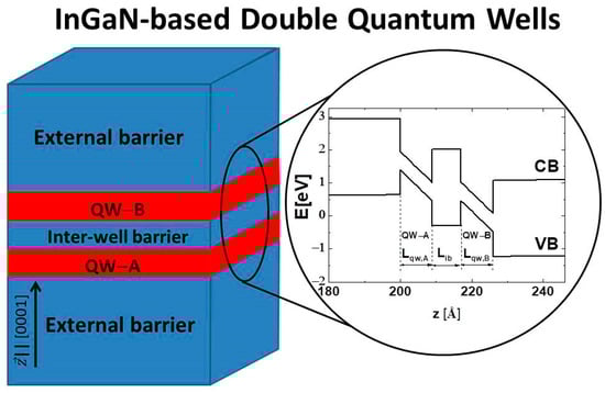
Figure 1.
Schematic representation of an InGaN-based DQW heterostructure. On the right side, the CB and VB edge profiles of an exemplary structure containing InN/In0.3292Ga0.6708N DQWs with , , and .
2. Theoretical Model
To study the polarization-induced phase transitions in InGaN-based DQWs, we employed the 8-band k∙p method combined with the nonlinear theory of elasticity and piezoelectricity. The application of the nonlinear theory of elasticity and piezoelectricity enabled us to accurately describe strain, piezoelectric polarization, and the built-in electric field, which is essential for obtaining an inversion of the CB and VB sub-bands. The applied k∙p method calculates quantum states in InGaN-based DQWs on the assumption that the effective SOI in InN is negative, which is crucial for determining the nature of the TPT and the properties of the TI phase.
We consider the structures (see Figure 1) in which the chemical compositions of the substrate, external barriers, and interwell barrier are the same, so these layers are unstrained. For simplicity, we also assume that the chemical compositions of both QWs are identical. Strain is only present in the QWs and is described by the following tensor:
where is the in-plane strain, is the out-of-plane strain, and denotes the biaxial relaxation coefficient [32]. The in-plane strain is determined by the well-known formula , where and are the lattice constants of the substrate and the QW material, respectively. We took the lattice constants for GaN and InN from [33] and assumed that for InGaN alloys, they linearly depend on composition [34]. The coefficient is usually determined using the linear theory of elasticity, which predicts that it is equal to , where and are the second-order elastic constants. This simple approach is, however, inaccurate when the strain is large [32,35]. Here, we apply a more general formula for the coefficient, which we derived in the framework of the third-order elasticity theory, as follows,
where and [24,32]. In the above formula, , , , and are the third-order elastic constants. For GaN and InN, we use the values of the elastic constants obtained from ab initio calculations, which were performed using the relationship between strain and the Helmholtz free energy density [32]. For InGaN alloys, we consider the nonlinear composition dependencies of the second-order elastic constants [35,36]. The composition dependencies of the third-order elastic constants are unknown for the group-III nitride alloys and, therefore, we use the linear approximation for these parameters in InGaN.
The built-in electric field in DQWs is calculated using a simple analytic model derived for a multilayer structure in [37]. This model is based on the assumption that the potential drop over the entire DQW structure, consisting of two external barriers, two QWs, and the interwell barrier, vanishes. The values of the built-in electric field in the corresponding layers of the DQW structure are given by the following formula:
where , , and denote the width of a layer, macroscopic polarization, and electric permittivity, respectively [37]. In this work, we dealt with the DQWs consisting of ultra-thin QWs and an interwell barrier, with widths expressed in MLs. The well widths depend on strain as follows,
where is the number of MLs, and denotes the lattice constant of the QW material. The factor of in Formula (4) originates from the fact that the wurtzite unit cell contains two MLs. We take the lattice constants for GaN and InN from [33] and assume that for InGaN alloys, they linearly depend on composition [34]. In QWs, the macroscopic polarization is the sum of the spontaneous polarization and the piezoelectric polarization , so it can be expressed by
where and are the first-order piezoelectric constants; , , , and are the second-order piezoelectric constants [38]. For unstrained barriers, the piezoelectric polarization is zero, and we have .
The electronic states in InGaN-based DQWs are calculated using the 8-band k·p Hamiltonian with relativistic and nonrelativistic linear-wave-vector terms, which were parametrized according to ab initio calculations performed using the quasiparticle self-consistent GW method [13,31]. The Hamiltonian is represented in a matrix form as follows:
where , , , , , , , , , , , , , and . The top valence band energy and energy gap are denoted by and , respectively; and describe the dispersion of the CB; whereas and are the Kane parameters [13,20]. The valence band parameters , , and were taken from [31] for GaN and InN, whereas for InGaN alloys, the linear approximation was applied. Additionally, the parameters were rescaled according to [20]. Strain and the built-in electric field were included in the Hamiltonian according to [39,40]. Then, replacing in the Hamiltonian by the operator , we have the 8-band Schrödinger-type equation,
where and are the energies and the envelope functions of the DQW states, respectively [13,20]. Because the material parameters depend on position in DQW structures, we use the standard symmetrization to ensure the Hermiticity of operators containing the products of functions and derivatives [20]. Equation (7) is solved using the standard finite element method [41].
3. Results and Discussion
We considered InxGa1−xN/GaN and InN/InyGa1−yN DQWs with the widths of individual QWs, , and , equal to two and three MLs, three and two MLs, and three and three MLs. We found that TPT can occur in these structures. On the other hand, in thinner DQWs, i.e., when and , the QCSE is too weak to induce the TPT, and only the NI phase appears. We assumed that the thickness of the external barriers (see Figure 1) is large, i.e., , because this makes the built-in electric field in QWs extremely large and the TPT easier to achieve [13].
3.1. InxGa1−xN/GaN DQWs
First, we investigated InxGa1-xN/GaN DQWs with , , and , which were grown on conventional GaN substrates. In Figure 2, we show the bulk energy gap, , and the subband dispersions for four distinct phases occurring in these structures. Figure 2a presents the as a function of the In content in the QWs. As in the case of single InxGa1−xN/GaN QWs [13,20], we observed the TPT and the NTPT, which were accompanied by the closing of . In a more detailed analysis, we observed that when the In content of the QWs, x, is below 0.96307, the DQW system is in the NI phase with the usual ordering of sub-bands (see Figure 2b). We would like to note that due to the negative SOI of InN, the highest light-hole (LH) sub-band with the symmetry is above the highest heavy-hole (HH) sub-band with the symmetry [13]. The names of the subbands reflect the dominant contribution of the CB, HH, and LH states around [19]. As the value of x increases, the energy gap of InxGa1−xN alloys decreases toward the bandgap of InN and, more importantly, the built-in electric field in the QWs increases, causing an inversion of the CB and LH sub-bands and the TPT from the NI to the TI (see Figure 2d). The TPT is mediated by the Weyl semimetal (WSM) (see Figure 2c) because the CB and LH sub-bands anticross at [13]. The amplitude of compressive in-plane strain in the QW layers at the TPT, denoted by , is about 9.71%. In the TI phase, the reaches a maximum value of . For x values larger than 0.96667, the vanishes due to the NTPT from the TI phase to the NTSM, arising from nonlocal overlapping between the sub-bands, as shown in Figure 2e [13,20].
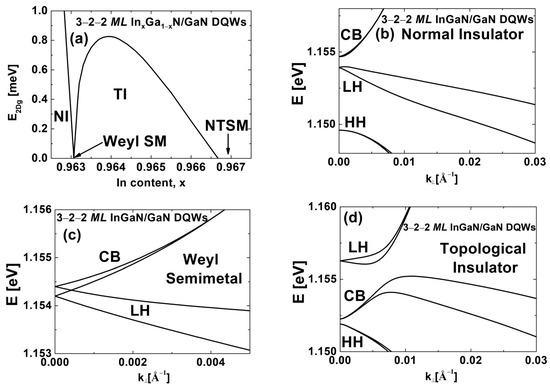
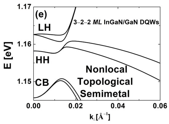
Figure 2.
(a) The for InxGa1−xN/GaN DQWs with , , and as a function of the In content in the QWs. (b–e) The sub-band dispersions for (b) the NI, (c) WSM, (d) TI, and (e) NTSM occurring in these DQWs.
Similar but slightly different results were obtained for InxGa1−xN/GaN DQWs with , , and . Figure 3a depicts the for these structures as a function of x. The TPT and the NTPT occurs for x = 0.95467 and x = 0.95812, respectively. The is 9.63% whereas the . The differences between the results presented in Figure 2a and Figure 3a originate from the fact that wurtzite structures have no center of inversion, and the crystallographic directions [0001] and [000-1] are not equivalent. In Figure 3b, we present the for the InxGa1−xN/GaN DQWs with , , and . Although we dealt with structures having identical widths of QWs, the observed phases remain essentially the same because the built-in electric field breaks the mirror symmetry of the DQW potential (see Figure 1). Therefore, the BG phase, which has been observed for symmetric HgTe/CdTe DQWs [29,30], does not appear in InxGa1−xN/GaN DQWs with the identical QW widths. Comparing the results shown in Figure 3b with those presented in Figure 2a and Figure 3a, we see that for the DQWs with both wells having three MLs, the TI phase is obtained with significantly less In content and, subsequently, less strain. In particular, the TPT and NTPT occur for x = 0.85573 and x = 0.85712, respectively. The is 8.71%, which is the advantage of these structures in terms of their epitaxial growth. Unfortunately, we predicted that the , which is almost twice as small as the DQWs considered in Figure 2a.
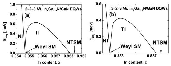
Figure 3.
The as a function of the In content in the QWs, for InxGa1−xN/GaN DQWs with (a) , , and ; and (b) , , and .
3.2. InN/InyGa1−yN DQWs
We extended our investigations to InN/InyGa1−yN DQWs. We assumed that these structures are pseudomorphically grown on metamorphic InyGa1−yN buffer layers or InyGa1−yN virtual substrates, which are used in optoelectronic devices [42,43,44,45]. In Figure 4, we present the for InN/InyGa1−yN DQWs with (a) and , (b) and , and (c) and . The width of the interwell barrier is . In all cases, we see the TPT from the NI to the TI via the WSM and the NTPT from the TI to the NTSM. These phase transitions are driven by an increase in the built-in electric field in QWs, due to a decrease in the In content in the barriers, y. For the structures presented in Figure 4a–c, the TPT occurs at a y equal to 0.09345, 0.10937, and 0.3311, respectively. Therefore, the values of are 9.10%, 8.94%, and 6.72%, and they are significantly smaller compared with the results obtained for the corresponding InxGa1−xN/GaN DQWs. Moreover, for InN/InyGa1−yN DQWs, we obtained higher values of , which are equal to , , and , for the structures considered in Figure 4a–c, respectively. Interestingly, in the case of InN/InyGa1−yN DQWs, we found that the smallest value of and, simultaneously, the largest , are for the structures with and . Therefore, these structures are the most attractive for experimental observation of the QSHE.
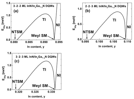
Figure 4.
The as a function of the In content in the barriers for InN/InyGa1−yN DQWs with (a) , , and ; (b) , , and ; and (c) , , and .
Finally, we studied the effect of increasing on the phase transitions in InN/InyGa1−yN DQWs. Figure 5 shows the for the structures with (a) , , and ; (b) , , and ; and (c) , , and . We see that the In content in the barriers for obtaining the TPT slightly decreases with increasing , so the increases with increasing . More importantly, one can see that both the and the window of the In content for the TI phase, , rapidly decrease with increasing . This effect is additionally demonstrated in Figure 6, where the and are presented as a function of . Figure 6a shows that with increasing , the decreases at a similar rate for all three series of DQWs. In Figure 6b, we see that the reduction in with increasing is slower for the structures with both QW widths being three MLs than for the structures with QW widths of two and three MLs. We also found that for sufficiently large , i.e., in Figure 5a,b and in Figure 5c, the TI phase does not appear. The value of at which the TI phase disappears is one ML larger for the series of DQWs with both QW widths being three MLs (Figure 5c), because for these structures, the is significantly larger than for the other two series of DQWs (Figure 5a,b), as is clearly seen in Figure 6a. In the cases where the TI phase disappears, we observed two novel phase transitions. First, we found the NTPT, from the NI to the nonlocal normal semimetal (NNSM), having the normal ordering of the CB and LH sub-bands. Then, the TPT occurs from the NNSM to the NTSM via the buried Weyl semimetal phase (BWSM) containing the Weyl points, which are buried in the LH sub-band. In Figure 7, we show the sub-band dispersions for all four phases ((a) NI, (b) NNSM, (c) BWSM, and (d) NTSM) in InN/InyGa1−yN DQWs with , , and , which occur in order of decreasing In content in the barriers. Similar results were obtained for the structures with , , and , and , , and . We would like to note that the NTPT from the NI to the NNSM was predicted for HgTe/CdTe QWs at high hydrostatic pressure [46]. To the best of our knowledge, the TPT from the NNSM to the NTSM via the BWSM was not discovered in any 2D structure.
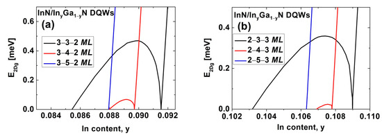
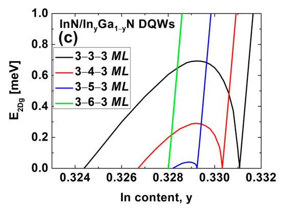
Figure 5.
The as a function of the In content in the barriers for InN/InyGa1−yN DQWs with (a) , , and ; (b) , , and ; and (c) , , and . The results obtained for different values of are marked with different colors.
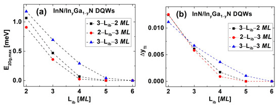
Figure 6.
The values of (a) and (b) for InN/InyGa1−yN DQWs as a function of . Squares represent DQWs with and , circles represent structures with and , and triangles correspond to the results for DQWs with and .
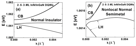
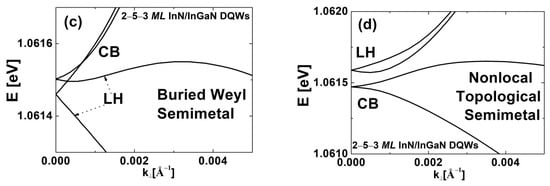
Figure 7.
The sub-band dispersions for (a) the NI, (b) NNSM, (c) BWSM, and (d) NTSM occurring in InN/InyGa1−yN DQWs with , , and . The phases appear in order of decreasing In content in the barriers.
4. Conclusions
We studied the phase transitions and the properties of the TI phase in InxGa1−xN/GaN and InN/InyGa1−yN DQWs, applying a realistic model based on the nonlinear theory of elasticity and piezoelectricity, and the eight-band k·p method with relativistic and nonrelativistic linear-wave-vector terms. Despite a rigorous assumption of a negative SOI in InN, we demonstrated that the TI phase can occur in InxGa1−xN/GaN and InN/InyGa1−yN DQWs when the widths of individual QWs are two and three MLs, and three and three MLs. In these structures, when the interwell barrier is sufficiently thin, we observed the TPT from the NI to the TI via the WSM, and the NTPT from the TI to the NTSM. We found that in InxGa1−xN/GaN DQWs, the is much smaller for the structures with both QW widths being three MLs than when the QW widths are two and three MLs, whereas in InN/InyGa1−yN DQWs, the opposite was true. For InN/InyGa1−yN DQWs with 3 ML QWs and the , the can reach about . Our calculations also revealed that both the and the rapidly decrease with increasing . We showed that for structures with above 5 or 6 MLs, the TI did not occur. In these structures, we found two novel phase transitions, namely the NTPT from the NI to the NNSM and the TPT from the NNSM to the NTSM, via the BWSM. We hope that these results will stimulate intensive theoretical and experimental studies toward achieving the TI phase in InGaN-based DQWs and will contribute to new applications of these prospective topological nanomaterials. Our work lays the groundwork for future investigations of the phase transitions in other QW systems fabricated from nontopological semiconductors, such as Ge/GaAs, InSb/CdTe, and ZnO/CdO, in which an inversion of the CB and VB sub-bands is achieved by the built-in electric field [47,48,49].
Author Contributions
Conceptualization, S.P.Ł.; methodology, S.P.Ł.; software, S.P.Ł.; validation, S.P.Ł.; formal analysis, S.P.Ł. and A.R.A.; investigation, S.P.Ł. and A.R.A.; writing—original draft preparation, S.P.Ł.; writing—review and editing, S.P.Ł. and A.R.A.; visualization, S.P.Ł.; supervision, S.P.Ł. All authors have read and agreed to the published version of the manuscript.
Funding
This research received no external funding.
Data Availability Statement
The data underlying this article are available from the corresponding author upon reasonable request.
Acknowledgments
S.P.Ł. would like to thank W. Bardyszewski from the Faculty of Physics, University of Warsaw for fruitful discussions concerning the topological phase transition in semiconductor quantum wells.
Conflicts of Interest
The authors declare no conflict of interest.
References
- Hasan, M.Z.; Kane, C.L. Colloquium: Topological insulators. Rev. Mod. Phys. 2010, 82, 3045. [Google Scholar] [CrossRef] [Green Version]
- Bansil, A.; Lin, H.; Das, T. Colloquium: Topological band theory. Rev. Mod. Phys. 2016, 88, 021004. [Google Scholar] [CrossRef] [Green Version]
- Sabater, C.; Gosálbez-Martínez, D.; Fernández-Rossier, J.; Rodrigo, J.G.; Untiedt, C.; Palacios, J.J. Topologically protected quantum transport in locally exfoliated bismuth at room temperature. Phys. Rev. Lett. 2013, 110, 176802. [Google Scholar] [CrossRef]
- Drozdov, I.K.; Alexandradinata, A.; Jeon, S.; Nadj-Perge, S.; Ji, H.; Cava, R.J.; Bernevig, B.A.; Yazdani, A. One-dimensional topological edge states of bismuth bilayers. Nat. Phys. 2014, 10, 664–669. [Google Scholar] [CrossRef] [Green Version]
- Wu, S.; Fatemi, V.; Gibson, Q.D.; Watanabe, K.; Taniguchi, T.; Cava, R.J.; Jarillo-Herrero, P. Observation of the quantum spin Hal effect up to 100 kelvin in a monolayer crystal. Science 2018, 359, 76–79. [Google Scholar] [CrossRef] [Green Version]
- Bernevig, B.A.; Hughes, T.L.; Zhang, S.C. Quantum spin Hall effect and topological phase transition in HgTe quantum wells. Science 2006, 314, 1757–1761. [Google Scholar] [CrossRef] [PubMed] [Green Version]
- Konig, M.; Wiedmann, S.; Brune, C.; Roth, A.; Buhmann, H.; Molenkamp, L.W.; Qi, X.L.; Zhang, S.C. Quantum spin Hall effect in HgTe quantum wells. Science 2007, 318, 766–770. [Google Scholar] [CrossRef] [PubMed] [Green Version]
- Liu, C.; Hughes, T.L.; Qi, X.L.; Wang, K.; Zhang, S.C. Quantum spin Hall effect in inverted type-II semiconductors. Phys. Rev. Lett. 2008, 100, 236601. [Google Scholar] [CrossRef]
- Knez, I.; Du, R.R.; Sullivan, G. Evidence for helical edge modes in inverted InAs/GaSb quantum wells. Phys. Rev. Lett. 2011, 107, 136603. [Google Scholar] [CrossRef] [Green Version]
- Kvon, Z.D.; Olshanetsky, E.B.; Novik, E.G.; Kozlov, D.A.; Mikhailov, N.N.; Parm, I.O.; Dvoretsky, S.A. Two-dimensional electron-hole system in HgTe-based quantum wells with surface orientation (112). Phys. Rev. B 2011, 83, 193304. [Google Scholar] [CrossRef]
- Prudkoglyad, V.A.; Olshanetsky, E.B.; Kvon, Z.D.; Pudalov, V.M.; Mikhailov, N.N.; Dvoretsky, S.A. Two-dimensional semimetal in HgTe quantum well under hydrostatic pressure. Phys. Rev. B 2018, 98, 155437. [Google Scholar] [CrossRef] [Green Version]
- Miao, M.; Yan, Q.; Van de Walle, C.G.; Lou, W.K.; Li, L.L.; Chang, K. Polarization-driven topological insulator transition in a GaN/InN/GaN quantum well. Phys. Rev. Lett. 2012, 109, 186803. [Google Scholar] [CrossRef] [PubMed] [Green Version]
- Łepkowski, S.P.; Bardyszewski, W. Topological insulator with negative spin-orbit coupling and transition between Weyl and Dirac semimetals in inGaN-based quantum wells. Sci. Rep. 2018, 8, 15403. [Google Scholar] [CrossRef] [PubMed]
- Leubner, P.; Lunczer, L.; Brune, C.; Buhmann, H.; Molenkamp, L.W. Strain engineering of the band gap of HgTe quantum wells using superlattice virtual substrates. Phys. Rev. Lett. 2016, 117, 086403. [Google Scholar] [CrossRef] [Green Version]
- Du, L.; Li, T.; Lou, W.; Wu, X.; Liu, X.; Han, Z.; Zhang, C.; Sullivan, G.; Ikhlassi, A.; Chang, K.; et al. R tuning edge states in strained-layer inAs/GaInSb quantum spin Hall insulators. Phys. Rev. Lett. 2017, 119, 056803. [Google Scholar] [CrossRef] [Green Version]
- Krishtopenko, S.S.; Ruffenach, S.; Gonzalez-posada, F.; Boissier, G.; Marcinkiewicz, M.; Fadeev, M.A.; Kadykov, A.M.; Rumyantsev, V.V.; Morozov, S.V.; Gavrilenko, V.I.; et al. Temperature-dependent terahertz spectroscopy of inverted-band three-layer InAs/GaSb/InAs quantum wells. Phys. Rev. B 2018, 97, 245419. [Google Scholar] [CrossRef]
- Olshanetsky, E.B.; Kvon, Z.D.; Gusev, G.M.; Levin, A.D.; Raichev, O.E.; Mikhailov, N.N.; Dvoretsky, S.A. Persistence of a two-dimensional topological insulator state in wide HgTe quantum wells. Phys. Rev. Lett. 2015, 114, 126802. [Google Scholar] [CrossRef] [Green Version]
- Bardyszewski, W.; Rodak, D.; Łepkowski, S.P. Magnetoconductance in InN/GaN quantum wells in topological insulator phase. EPL 2017, 118, 27001. [Google Scholar] [CrossRef]
- Łepkowski, S.P.; Bardyszewski, W.; Rodak, D. Polarization-induced band inversion in In-rich InGaN/GaN quantum wells. Acta Phys. Pol. A 2014, 126, 1154–1155. [Google Scholar] [CrossRef]
- Łepkowski, S.P.; Bardyszewski, W. Topological phase transition and evolution of edge states in In-rich InGaN/GaN quantum wells under hydrostatic pressure. J. Phys. Condens. Matter 2017, 29, 055702. [Google Scholar] [CrossRef]
- Kusakabe, K.; Hashimoto, N.; Itoi, T.; Wang, K.; Imai, D.; Yoshikawa, A. Growth kinetics and structural perfection of (InN)1/(GaN)1-20 short-period superlattices on +c-GaN template in dynamic atomic layer epitaxy. Appl. Phys. Lett. 2016, 108, 152107. [Google Scholar] [CrossRef]
- Dimitrakopulos, G.P.; Vasileiadis, I.G.; Smalc-Koziorowska, J.; Kret, S.; Dimakis, E.; Florini, N.; Kehagias, T.; Suski, T.; Karakostas, T.; Moustakas, T.D.; et al. Compositional and strain analysis of In(Ga)N/GaN short period superlattices. J. Appl. Phys. 2018, 123, 024304. [Google Scholar] [CrossRef]
- Vasileiadis, I.G.; Lymperakis, L.; Adikimenakis, A.; Gkotinakos, A.; Devulapalli, V.; Liebscher, C.H.; Androulidaki, M.; Hubner, R.; Karakostas, T.; Georgakilas, A.; et al. Substitutional synthesis of sub-nanometer InGaN/GaN quantum wells with high indium content. Sci. Rep. 2021, 11, 20606. [Google Scholar] [CrossRef] [PubMed]
- Łepkowski, S.P.; Bardyszewski, W. Anomalous Rashba spin-orbit interaction in electrically controlled topological insulator based on InN/GaN quantum wells. J. Phys. Condens. Matter 2017, 29, 195702, Corrigendum in J. Phys. Condens. Matter 2020, 33, 119501. [Google Scholar] [CrossRef]
- Hu, G.; Zhang, Y.; Li, L.; Wang, Z.L. Piezotronic transistor based on topological insulators. ACS Nano 2017, 12, 779–785. [Google Scholar] [CrossRef]
- Dan, M.; Hu, G.; Li, I.; Zhang, Y. High performance piezotronic logic nanodevices based on GaN/InN/GaN topological insulator. Nano Energy 2018, 50, 544–551. [Google Scholar] [CrossRef] [Green Version]
- Litvinov, V.I. Quantum anomalous Hall state with Chern number C = 2 in wurtzite quantum wells. Phys. Rev. B 2021, 104, 245304. [Google Scholar] [CrossRef]
- Michetti, P.; Budich, J.C.; Novik, E.G.; Recher, P. Tunable quantum spin Hall effect in double quantum wells. Phys. Rev. B 2012, 85, 125309. [Google Scholar] [CrossRef] [Green Version]
- Krishtopenko, S.S.; Knap, W.; Teppe, F. Phase transitions in two tunnel-coupled HgTe quantum wells: Bilayer graphene analogy and beyond. Sci. Rep. 2016, 6, 30755. [Google Scholar] [CrossRef] [Green Version]
- Gusev, G.M.; Olshanetsky, E.B.; Hernandez, F.G.G.; Raichev, O.E.; Mikhailov, N.N.; Dvoretsky, S.A. Two-dimensional topological insulator state in double HgTe quantum well. Phys. Rev. B 2020, 101, 241302. [Google Scholar] [CrossRef]
- Punya, A.; Lambrecht, W.R.L. Valence band effective-mass Hamiltonians for the group-III nitrides from quasiparticle self-consistent GW band structures. Phys. Rev. B 2012, 85, 195147. [Google Scholar] [CrossRef] [Green Version]
- Łepkowski, S.P.; Anwar, A.R. Third-order elastic constants and biaxial relaxation coefficient in wurtzite group-III nitrides by hybrid-density functional theory calculations. J. Phys. Condens. Matter 2021, 33, 355402. [Google Scholar] [CrossRef] [PubMed]
- Vurgaftman, I.; Meyer, J.R. Band parameters for nitrogen-containing semiconductors. J. Appl. Phys. 2003, 94, 3675. [Google Scholar] [CrossRef]
- Gorczyca, I.; Łepkowski, S.P.; Suski, T.; Christensen, N.E.; Svane, A. Influence of indium clustering on the band structure of semiconducting ternary and quaternary nitride alloys. Phys. Rev. B 2009, 80, 075202. [Google Scholar] [CrossRef]
- Łepkowski, S.P.; Anwar, A.R. Biaxial relaxation coefficient in group-III nitride quantum wells and thin films. Acta Phys. Pol. A 2022, 141, 130–134. [Google Scholar] [CrossRef]
- Łepkowski, S.P. Inapplicability of Martin transformation to elastic constants of zinc-blende and wurtzite group-III nitride alloys. J. Appl. Phys. 2015, 117, 105703. [Google Scholar] [CrossRef]
- Bernardini, F.; Fiorentini, V. Spontaneous versus piezoelectric polarization in III-V nitrides: Conceptual aspects and practical consequences. Phys. Stat. Sol. 1999, 216, 391–398. [Google Scholar] [CrossRef] [Green Version]
- Prodhomme, P.-Y.; Beya-Wakata, A.; Bester, G. Nonlinear piezoelectricity in wurtzite semiconductors. Phys. Rev. B 2013, 88, 121304. [Google Scholar] [CrossRef]
- Chuang, S.L.; Chang, C.S. k∙p method for strained wurtzite semiconductors. Phys. Rev. B 1996, 54, 2491–2504. [Google Scholar] [CrossRef]
- Łepkowski, S.P.; Gorczyca, I.; Stefańska-Skrobas, K.; Christensen, N.E.; Svane, A. Deformation potentials in AlGaN and InGaN alloys and their impact on optical polarization properties of nitride quantum wells. Phys. Rev. B 2013, 88, 081202. [Google Scholar] [CrossRef]
- Huebner, K.H.; Thornton, E.A. The Finite Element Method for Engineers; Wiley: New York, NY, USA, 1982; pp. 22–123. [Google Scholar]
- Fabien, C.A.M.; Gunning, B.P.; Doolittle, W.A.; Fischer, A.M.; Wei, Y.O.; Xie, H.; Ponce, F.A. Low-temperature growth of InGaN films over the entire composition range by MBE. J. Cryst. Growth 2015, 425, 115–118. [Google Scholar] [CrossRef] [Green Version]
- Daubler, J.; Passow, T.; Aidam, R.; Kohler, K.; Kirste, L.; Kunzer, M.; Wagner, J. Long wavelength emitting GaInN quantum wells on metamorphic GaInN buffer layers with enlarged in-plane lattice parameter. Appl. Phys. Lett. 2014, 105, 111111. [Google Scholar] [CrossRef]
- Even, A.; Laval, G.; Ledoux, O.; Ferret, P.; Sotta, D.; Guiot, E.; Levy, F.; Robin, I.C.; Dussaigne, A. Enhanced In incorporation in full InGaN heterostructure grown on relaxed InGaN pseudo-substrate. Appl. Phys. Lett. 2017, 110, 262103. [Google Scholar] [CrossRef]
- Anwar, A.R.; Sajjad, M.T.; Johar, M.A.; Hernandez-Gutierrez, C.A.; Usman, M.; Łepkowski, S.P. Recent progress in micro-LED based display technologies. Laser Photonics Rev. 2022, 16, 2100427. [Google Scholar] [CrossRef]
- Krishtopenko, S.S.; Yahniuk, I.; But, D.B.; Gavrilenko, V.I.; Knap, W.; Teppe, F. Pressure- and temperature-driven phase transitions in HgTe quantum wells. Phys. Rev. B 2016, 94, 245402. [Google Scholar] [CrossRef] [Green Version]
- Zhang, D.; Lou, W.; Miao, M.; Zhang, S.C.; Chang, K. Interface-induced topological insulator transition in GaAs/Ge/GaAs quantum wells. Phys. Rev. Lett. 2013, 111, 156402. [Google Scholar] [CrossRef] [PubMed] [Green Version]
- Liu, Q.; Zhang, X.; Abdalla, L.B.; Zunger, A. Transforming common III-V and II-VI semiconductor compounds into topological heterostructures: The case of CdTe/InSb superlattices. Adv. Funct. Mater. 2016, 26, 3259. [Google Scholar] [CrossRef] [Green Version]
- Hu, G.; Zhang, Y. Quantum piezotronic devices based on ZnO/CdO quantum well topological insulator. Nano Energy 2020, 77, 105154. [Google Scholar] [CrossRef]
Publisher’s Note: MDPI stays neutral with regard to jurisdictional claims in published maps and institutional affiliations. |
© 2022 by the authors. Licensee MDPI, Basel, Switzerland. This article is an open access article distributed under the terms and conditions of the Creative Commons Attribution (CC BY) license (https://creativecommons.org/licenses/by/4.0/).