Abstract
As extraordinary topological insulators, 2D bismuth telluride (Bi2Te3) nanosheets have been synthesized and controlled with a few-layer structure by a facile and fast solvothermal process. The detail-oriented growth evolution of 2D Bi2Te3 in an ethylene glycol reducing solution is discovered and recorded for direct observation of the liquid–solid interactions through the use of environmental SEM. At the initial synthesis stage, Te nanowires are rapidly synthesized and observed in solution. In the next stage, Bi nanoclusters slowly adhere to the Te nanowires and react to form hierarchical Te-Bi2Te3 nanostructured materials. Additionally, the Te nanowires shorten in-plane in an orderly manner, while the Bi2Te3 nanosheets exhibit directional out-of-plane epitaxial growth. In the last procedure, Bi2Te3 nanosheets with a clear hexagonal appearance can be largely obtained. Experiments performed under these rigorous conditions require careful consideration of the temperature, time, and alkaline environment for each reaction process. In addition, the yield of a wider and thinner Bi2Te3 nanosheet is synthesized by manipulating the crystal growth with an optimal alkaline concentration, which is found through statistical analysis of the AFM results. In the UV–Vis–NIR spectroscopy results, the main peak in the spectrum tends to redshift, while the other peak in the ultraviolet range decreases during Bi2Te3 nanosheet synthesis, facilitating a rapid understanding of the trends in the morphological evolution of the Bi2Te3 materials in solution. By rationalizing the above observations, we are the first to report the success of environmental SEM, HAADF-STEM, and UV–Vis–NIR spectroscopy for confirming the Bi2Te3 nanosheet formation mechanism and the physical properties in the solvent media. This research promotes the future optimization of promising Bi2Te3 nanomaterials that can be used in the fabrication of thermoelectric and topological components.
1. Introduction
Two-dimensional layer-structured metal chalcogenides, such as bismuth telluride (Bi2Te3) thermoelectrics, have attracted considerable attention for their unique applications during the past decades because they are functional materials that can be broadly applied as topological insulators [1,2], 2D photodetectors [3,4,5] and electrodes [6], and energy harvesters [7,8,9,10], including the latest innovations from our recent research on nanogenerator achievements [10]. The crystal structure of Bi2Te3 thermoelectrics belongs to the rhombohedral (Rm) space group, which is described by a hexagonal unit cell with lattice constants of a = 1.041 nm and c = 3.029 nm and a stacking sequence of Te(1)-Bi-Te(2)-Bi-Te(1) to form a quintuple layer. It should be noted that the bonding between two quintuple layers, Te(1)-Te(1), is bonded by weak van der Waals interactions, similar to two-dimensional materials, thus leading to the observation of numerous exciting physical phenomena and exotic properties [11,12].
Furthermore, ultrathin Bi2Te3 structured materials are classified as topological insulators, as they generally have unique topological properties because the band structure of the Bi2Te3 surface exhibits a single nondegenerate Dirac cone, resulting in high conductivity, high electron mobility, and a switchable electronic surface current with low energy loss, which is an attractive property in many industrial fields [6,13]. On the other hand, Bi2Te3 materials also exhibit outstanding thermoelectric properties, so a variety of synthesis processes have been developed, including a common chemical vapor deposition (CVD) process applied to the synthesis of Bi2Te3 nanosheets [14,15,16], and the other much more precise controlling method, namely, molecular beam epitaxial (MBE) growth, which has also been utilized for synthesizing high-quality Bi2Te3 ultrathin films [17,18]. Although the quality and thickness of Bi2Te3 thin films can be effectively controlled by using these processes, to overcome the extremely costly production of MBE and CVD synthesis processes, such as expensive vacuum facilities and sample size limitations in the systems, a fast and simple solution process has been explored to form inexpensive, large, and uniform Bi2Te3 ultrathin films [12,19,20].
However, the undesirable intermediate product and the different shapes of the Bi2Te3-Te hierarchical-structured nanomaterial composed of Bi2Te3 nanosheets and Te nanorods have also been obtained by controlling the rates of the competing reactions for the formation of Bi2Te3 and Te during the experimental process through two-step solvothermal methods [21]. This three-dimensional hierarchical Bi2Te3-Te heterostructure in which the chemical composition changes with the position will affect the qualities of the Bi2Te3 ultrathin film grown by chemical synthesis; thus, it is necessary to prevent the formation of the intermediate hierarchical Bi2Te3-Te heterojunction to effectively control the growth of the Bi2Te3 ultrathin film during synthesis. Bi2Te3-Te hierarchical-structured nanomaterials have also been fabricated by adding sucrose as a template and ethylene glycol (EG) as a reducing agent so that different sizes of heterostructured nanomaterials can be obtained [21].
The detail-oriented description of the formation of Bi2Te3 hexagonal nanosheets has seldom been reported thus far, but it is believed that determining the detailed growth mechanism of Bi2Te3 nanosheets is meaningful for further application. In this study, the detailed mechanism of forming Bi2Te3 nanosheets using a simple one-pot solvothermal method is discovered, and the role of different times, temperatures, and alkaline concentrations are also investigated thoroughly. We also examine and rationalize the shape/aspect ratio of the Bi2Te3 nanosheets under different growth conditions by using a statistical method with atomic force microscopy (AFM) and ultraviolet–visible–near–infrared (UV–Vis–NIR) spectroscopy. The experimental direct and indirect observation results via environmental scanning electron microscopy (SEM), high resolution transmission electron microscope (HRTEM), and high-angle annular dark-field scanning transmission electron microscopy (HAADF-STEM) mapping images show that Bi2Te3-Te hierarchical nanomaterials will be generated briefly in solution during the formation of Bi2Te3 nanosheets. These useful research results indicate that prospective materials for nanogenerators and thermoelectric applications can be further developed in the future.
2. Materials and Methods
2.1. Preparation and Synthesis of the Bi2Te3 Hexagonal Nanosheets
Bismuth nitrate pentahydrate (Bi(NO3)3·5H2O, 0.2 mmol, 99.99%, Acros, NJ, USA), sodium tellurite (Na2TeO3, 0.3 mmol, 99.5%, Alfa, Turin, Italy), polyvinyl pyrrolidone (2 mmol, Mw 40,000, Alfa) and a specific quantity of sodium hydroxide (NaOH, 97%, Showa, Tokyo, Japan) were dissolved in 10 mL of ethylene glycol (C2H4(OH)2, 99.8%, Sigma-Aldrich, St. Louis, MO, USA). To examine the role of chemical reactions in alkaline solutions, a variety of precise concentrations of NaOH with 0.2 M, 0.3 M, 0.4 M, and 0.5 M were prepared. The mixture required a heat reflux setup in a three-necked flask, which was heated and maintained at several controllable temperatures of 170 °C, 180 °C, and 190 °C. The synthesized sample was centrifuged at 8000 rpm for 8 min with a blended solvent of 5 mL of acetone (99.5%, Acros) and 10 mL of isopropanol (99%, Acros). The precipitates were dispersed and cleaned by an ultrasonicator three times. The final synthesized product was cleared by centrifugation and then dropped on a silicon substrate by using a spin-coating method to conduct further characterization. The experimental procedures are illustrated in Figure 1.
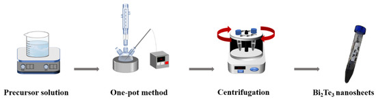
Figure 1.
Schematic showing the growth process of the Bi2Te3 hexagonal nanosheets.
2.2. Material Characterization
For material characterization, X-ray diffraction (XRD, D8 Bruker) with a Cu-Kα radiation source (λ = 1.54 Å) and scanning electron microscopy (SEM, JEOL JSM-6330) equipped with an energy dispersive spectroscopy (silicon drift detector (SDD) EDS, AMETEK EDAX Genesis PV9840) detector at different takeoff angles (40°) were utilized to understand the crystal structure, morphology, and composition of the Bi2Te3 nanosheets. The scanning range was from 10° to 70°, and the scanning rate was 0.0125° per second in the XRD measurement. The software (MDI Jade 6.5) was used for XRD pattern analysis. The accelerating voltages were used in SEM between 10 and 15 kV. Next, the detailed high-resolution lattice structure and nanoscale elemental distribution of the Bi2Te3 nanosheets were further characterized by ultrahigh vacuum high-resolution scanning transmission electron microscopy (STEM, FEI Tecnai F20 G2) at an accelerating voltage of 200 keV with a point-to-point resolution of 0.14 nm and equipped with a high-angle annular dark field (HAADF) and EDS (SDD, OXFORD INCA x-stream) detector at different takeoff angles (15°). The EDS maps were formed using the X-ray lines: Bi-M and Te-L. For real-time liquid material analysis, environmental SEM testing techniques for observing material formation were investigated through a single-use sealable carrier with a microchannel inside (Aquarius Kit, FlowVIEW Tek). The experiment used nanofilm fabricated by microelectromechanical systems (MEMS) to create an atmospheric environment during SEM, thereby keeping the liquid samples in their original state. This sealable carrier is precise, facilitating the simultaneous direct observation of analytical results, such as the particle dispersity/aggregate, shape evolution, and composition distributions.
The synthesized sample was used to identify the thickness and size of the material with atomic force microscopy (AFM, Hitachi 5000). In this statistical investigation, ultrathin Bi2Te3 sheets were extracted in a dilute solvent by a spin-coating method, and thirty pieces of Bi2Te3 nanosheets were regularly recorded to determine the average correlation between the thickness and diameter by AFM. For the non-destructive chemical analysis technique, absorption spectrum analysis was performed with ultraviolet–visible–near-infrared (UV–Vis–NIR) spectroscopy (JASCO, V-770 EX) to measure the physical properties and morphological evolution of materials.
3. Results
3.1. Synthesis of the Bi2Te3 Nanosheets and Bi2Te3-Te Hierarchical Nanostructure under Different Temperature and Alkaline Conditions
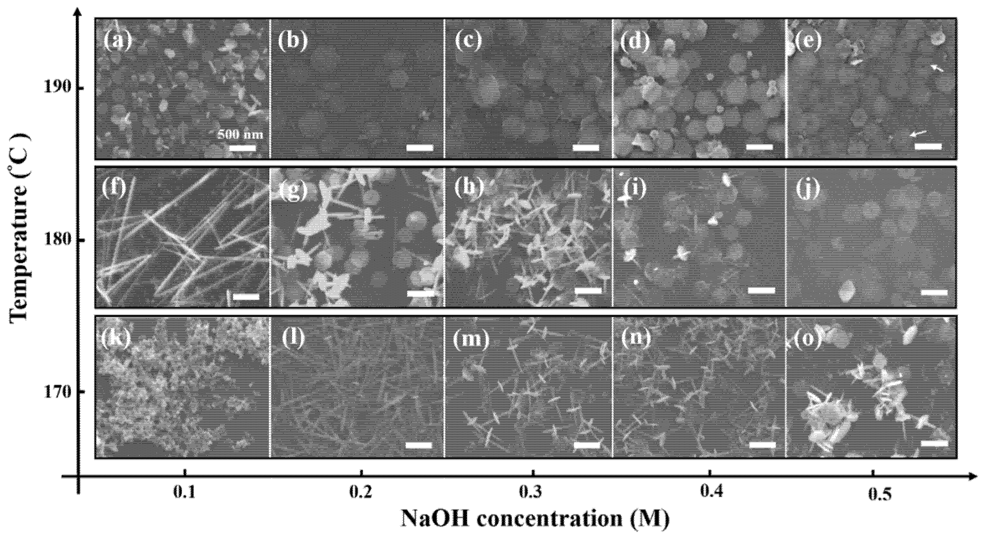
To present the influence of temperature, the synthesis products with different alkaline concentrations at 170–190 °C for 1 h are displayed in Figure 2. The growth mechanism of the Bi2Te3 nanosheets at different temperatures (170–190 °C), indicates a higher reaction rate at both higher alkaline concentration and reaction temperature. Interestingly, the morphology of the Bi2Te3 nanosheets is completely different when reacted with different concentrations in the reaction temperature range of 170 °C to 190 °C, as shown in Figure 2.
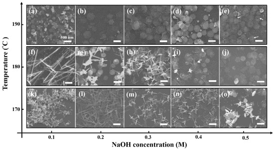
Figure 2.
Investigating the correlation of concentration on the reaction temperature. The morphologies of the Bi2Te3 hexagonal nanosheets with different concentrations of NaOH reacting at (a–e) 190 °C, (f–j) 180 °C, and (k–o) 170 °C for 1 h. The concentrations of NaOH are arranged systematically (a,f,k) 0.1 M, (b,g,l) 0.2 M, (c,h,m) 0.3 M, (d,i,n) 0.4 M, and (e,j,o) 0.5 M. The scale bar is 500 nm. The ET detector is a secondary electron detector used in SEM.
With careful examination of the SEM images (Figure 2a–e), it can be found clearly that well synthesized hexagonal nanosheets are obtained in 0.1M, 0.2 M, 0.3 M, 0.4 M, and 0.5 M NaOH solution. Note that an increasing number of nuclei are formed in the higher alkaline concentration solution so that large quantities of Bi2Te3 nanosheets are consequently produced. Interestingly, some slight nanopores (10 nm in diameter) are observed in the middle of the Bi2Te3 nanosheets that reacted with 0.5 M NaOH at 190 °C for 1 h. The results are indicated by the white arrows shown in Figure 2e. Previous literature reported that nanopores were found in the middle of Bi2Te3 nanosheets below a reaction temperature of 190 °C using the solvothermal method; however, no nanopores appeared in the Bi2Te3 nanosheets above a relatively high reaction temperature of 200 °C [12]. The pores provide important evidence for growth from nanowires to nanosheets. In 0.5 M NaOH solution, Te atoms diffused from the nanowires to form Bi2Te3 nanosheets, which were intercepted because the reaction time of 1h was not sufficient. Once the reaction time is extended to 3h, the Bi and Te atoms will diffuse uniformly to the entire hexagonal sheet until the final hole is repaired, as shown in Figure S1 in the Supplementary File.
In Figure 2f, there are many fairly tiny and smooth nanowires with diameters of 80–100 nm and no complete hexagonal Bi2Te3 nanosheets. However, many Bi2Te3-Te hierarchical nanostructures, which exhibit a lot of Bi2Te3 nanosheets perpendicular to the Te nanowires, are observed and recorded in Figure 2g–i and Figure 2l–o, representing the batch experiments of 0.2 M, 0.3 M, and 0.4 M NaOH reacted at 170 °C and 180 °C for 1 h. Notably, no Bi2Te3 nanosheets and Te nanowires could be observed in Figure 2k.
AFM images show the average distribution of the thickness and size of thirty pieces of Bi2Te3 nanosheets synthesized at 190 °C for different reaction times, namely, 1 h (Figure 3a) and 3 h (Figure 3b). The completed data of the statistical mean size and thickness distribution of Bi2Te3 nanosheets are summarized in Figures S2 and S3 in the Supplementary File. When the reaction time is increased, the material tends to grow laterally. In Figure 3c,d, the statistical results show that when the average diameter of Bi2Te3 nanosheets is significantly increased, the average thickness will be thinner. These measurement results are very important for future practical applications. A previous report stated that some metal chalcogenide nanosheets can be studied with AFM in terms of their internal size and thickness. It indicates a larger size-to-thickness ratio during synthesis; thus, the formation of morphology is dominated by nanosheets [22].
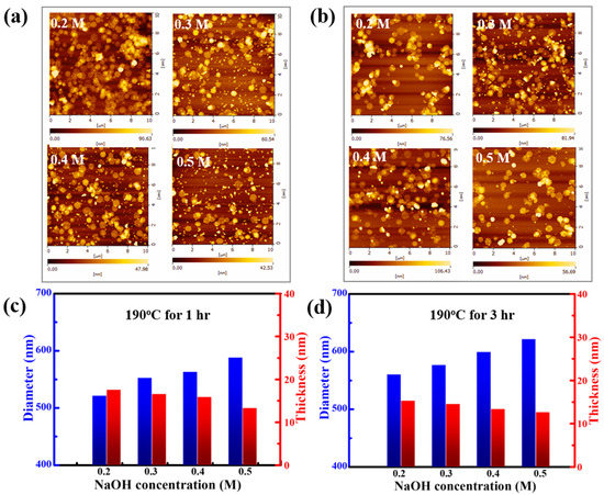
Figure 3.
AFM images of the Bi2Te3 hexagonal nanosheets synthesized at 190 °C at various concentrations of 0.2 M, 0.3 M, 0.4 M, and 0.5 M NaOH for (a) 1 h and (b) 3 h, respectively. Statistical histogram of the mean size and thickness distribution of Bi2Te3 nanosheets at different NaOH concentrations for (c) 1 h and (d) 3 h at 190 °C, respectively.
According to the statistical results of the AFM measurements, even though the reaction time is increased from 1 h to 3 h, the average thickness of an individual Bi2Te3 nanosheet is approximately 15 nm. However, the average thickness of the Bi2Te3 nanosheets tends to become thinner with increasing concentrations of NaOH. The overall thickness of the Bi2Te3 nanosheet tends to become thicker while the reaction time is increased from 1 h to 3 h, and the average of the Bi2Te3 nanosheets decreases from 13 nm to 16 nm. In terms of size, the diameter distribution of the Bi2Te3 nanosheets is approximately 520–620 nm. It can be observed that the average diameter of the Bi2Te3 nanosheets becomes larger with a higher NaOH concentration, and the average size of the Bi2Te3 nanosheets that are produced after reacting at 190 °C for 1 h and 3 h increases from 520 nm to 580 nm and from 560 nm to 620 nm, respectively. The AFM results show that the overall size of the Bi2Te3 nanosheets tends to increase as the reaction time is extended from 1 h to 3 h.
3.2. Suggested Mechanism and UV–Vis–NIR Spectroscopy Results of Bi2Te3-Te Hierarchical Nanostructure and Bi2Te3 Nanosheets
According to the results of SEM in Figure 2, a perspective self-assembly mechanism of the Bi2Te3 hierarchical nanostructure is illustrated in Figure 4. In this study, Te nanowires are observed to first synthesize in the solution before the bismuth nitrate pentahydrate solution is injected to form the hierarchical Bi2Te3-Te heterogeneous structure. Furthermore, a simultaneous synthesis process presents the transformation from pure chalcogen and metal particles to form metal chalcogenides. This finding is similar to the previously investigated nonstoichiometric nucleation and growth mechanism of two-dimensional nanosheets of layer-structured metal chalcogenides [23,24].
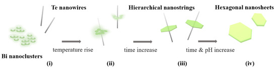
Figure 4.
Suggested self-assembly mechanism of the Bi2Te3 hierarchical nanostructure. (i) Te nanowire/Bi nanoclusters, (ii) Te nanowire/Bi2Te3 platelet composites, (iii) Bi2Te3 hierarchical structure, and (iv) Bi2Te3 nanosheets.
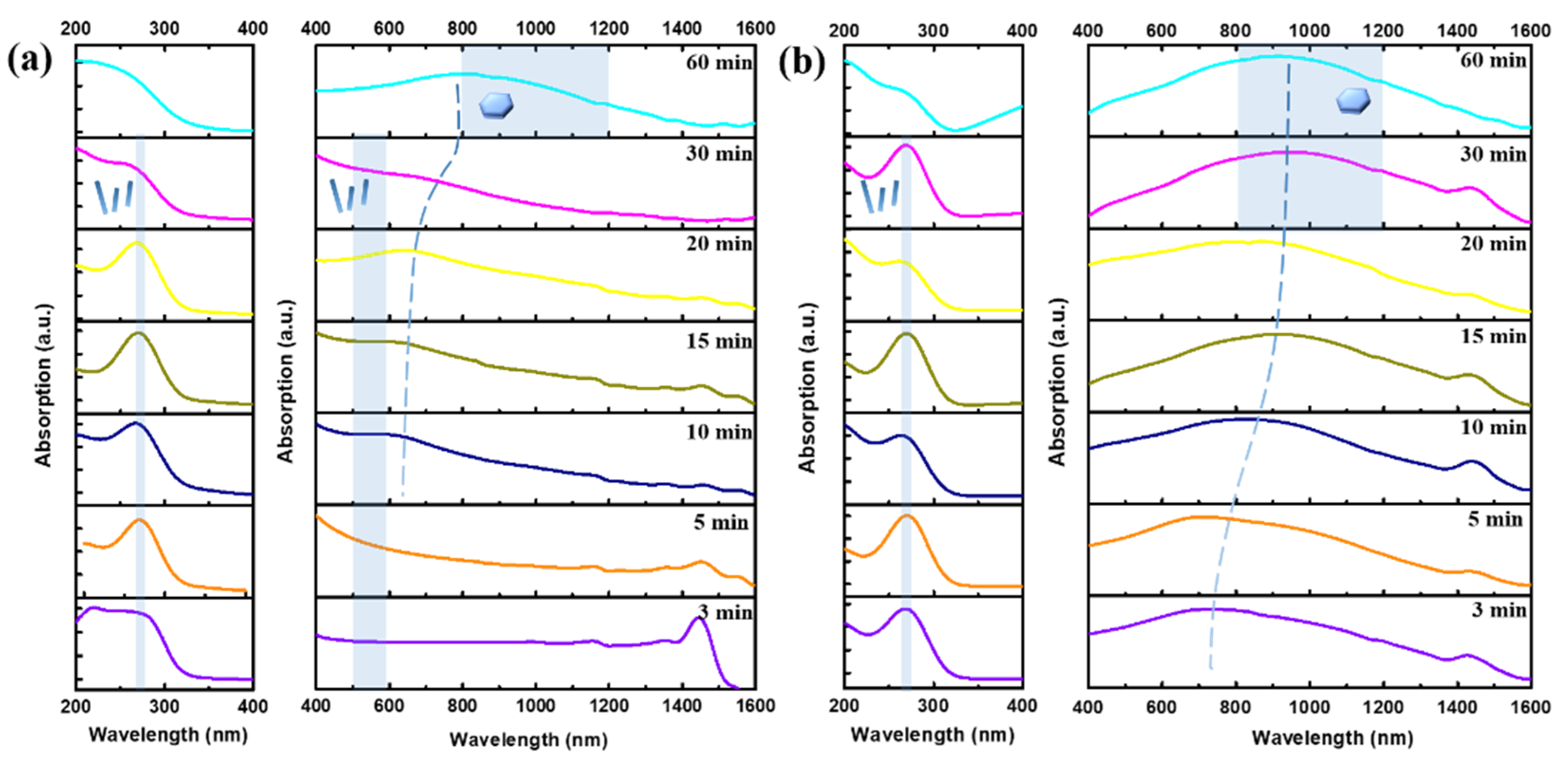
To study the growth evolution of Bi2Te3 nanosheets and the correlation of their optical properties, UV–Vis–NIR absorption spectroscopy was subsequently adopted with samples synthesized in 0.4 M NaOH reacting at 170 °C and 190 °C for seven different reaction periods of 3, 5, 10, 15, 20, 30, and 60 min, as shown in Figure 5a,b, respectively.
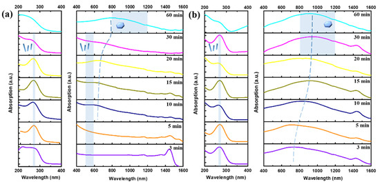
Figure 5.
UV–Vis–NIR absorption measurements were obtained over a reaction time of 3, 5, 10, 15, 20, 30, and 60 min at (a) 170 °C and (b) 190 °C in 0.4 M NaOH.
In the SEM results for different reaction time (Figure S4 in the Supplementary File), it can be seen that Te nanowires appear at 170 °C after 10 min, as shown in Figure S4d–f; additionally, few Bi2Te3 nanosheets are formed and attached to the Te nanowires. When the reaction time is extended to 30 min, a high density and yield of Bi2Te3 hierarchical heterostructure are obtained. From the related literature on the absorption spectrum of Te nanowires, a significant absorption peak exists at 280 nm and 630 nm [25]. The reason is the electron transitions from the valence band (p-lone pair VB3) to the conduction band (p-antibonding CB1) [25]. Thus, it is possible to determine that the absorption peaks at 280 nm and 630 nm in Figure 5a are caused by the Te nanowires. The reason for the occurrence of a red shifting absorption peak recorded from 20 min to 60 min during the growth process is that the Te atoms and Bi atoms gradually undergo a chemical reaction to form Bi2Te3 nanosheets as shown in Figure 5a.
In Figure S5a–d, it can be seen that the morphology evolution from Bi2Te3-Te hierarchical nanostructure to predominantly Bi2Te3 nanosheets appeared after 3 min to 15 min at 190 °C, which leads to the occurrence of a red shifting absorption peak during the initial growth process. Furthermore, it can be observed that only the Bi2Te3 nanosheets are present after the reaction lasts for 20 min, and no other types of nanostructured materials are presented in Figure S5e,f, which shows a stable broad absorption in the range of 800~1000 nm as shown in Figure 5b. It is known from the literature that the characteristic absorption spectrum of Bi2Te3 nanosheets is a broad absorption peak from visible light to infrared light [20,25,26].
As seen from the measurement results in Figure 5b, the absorption peak at a wavelength of 650 nm in the three-minute experiment appears to be redshifted to the infrared light range (800~1000 nm). Some studies reported that the incident-free electrons were absorbed on the surface of Bi2Te3 nanosheets and interacted to generate plasmon resonance, thus causing a large amount of light absorption in the infrared light range [20,26]. In addition, the absorption peak broadens for two reasons. First, the surface of Bi2Te3 nanosheets has three hexagonal surface plasmon modes. According to the electron energy loss spectroscopy (EELS) experimental results in the literature, the energy is located at 1.6, 2.1, and 3.1 eV, which relates to the size distribution of Bi2Te3 nanosheets [20,26]. Herein, it can be confirmed that the growth mechanisms at both 170 °C and 190 °C are similar, but the only difference is the reaction rate.
3.3. TEM Characterization of the Predicted Growth Mechanism and Chemical Reaction Formula of the Bi2Te3 Nanosheets and Bi2Te3-Te Hierarchical Nanostructure
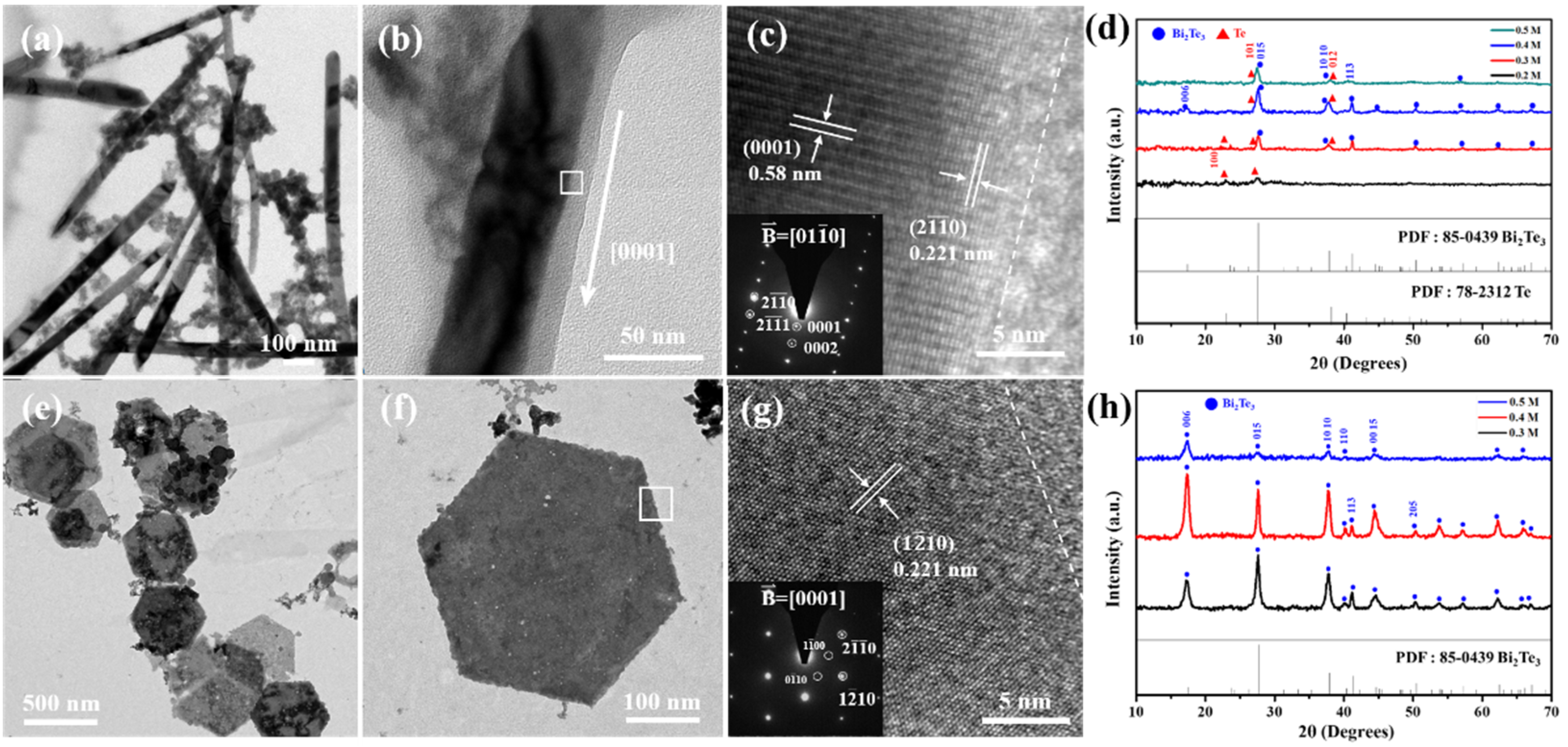
The detailed TEM characterization is investigated in Figure 6, in which Figure 6a shows the bright-field image of the Te nanowires synthesized at 170 °C with 0.2 M NaOH for 1 h, and the representative XRD patterns of the Te nanowires belong to a hexagonal structure with space group P3121, as shown in Figure 6d. It is also observed that many Bi nanoclusters are entangled with the nanowires in Figure 6a. In Figure 6b,c, the higher magnification of the bright-field image and its corresponding high-resolution TEM image present the nanowire that grew in the [0001] direction. Figure 6c also shows a length of 0.221 nm of the corresponding (20) d-spacing, and the SAED patterns of the Te nanowire are recorded along with the [010] zone axis.
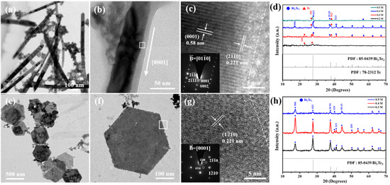
Figure 6.
TEM was used to investigate the role of Te nanowires and Bi2Te3 hexagonal nanosheets. Bright-field images of all Te nanowires and Bi2Te3 nanosheets. The Te nanowires were synthesized in 0.2 M NaOH solvent at 170 °C for 1 h. (a) Lower magnification TEM bright-field image of pure Te nanowires with diameters of 80–100 nm and (b) high magnification indicating the growth direction of the nanowire along with the [0001] zone. (c) HRTEM image and the corresponding SAED patterns of the white square in (b). (d) XRD patterns of the Te-Bi2Te3 nanocomposites reacted with various NaOH concentrations at 170 °C. The Bi2Te3 nanosheets were synthesized in 0.3 M NaOH solvent at 190 °C for 1 h. (e) Lower magnification TEM bright-field image of Bi2Te3 nanosheets with diameters of 500 nm and (f) high magnification image of an individual Bi2Te3 nanosheet existing on the {100} plane. (g) HRTEM and corresponding SAED pattern images are shown in the white square in (f). (h) XRD patterns of the hexagonal Bi2Te3 nanosheets reacted with various NaOH concentrations at 190 °C for 1 h.
On the other hand, the many pieces of Bi2Te3 nanosheets from reaction with 0.3 M NaOH at 190 °C for 1 h are presented in Figure 6e, and the morphology of an individual Bi2Te3 nanosheet presents a good hexagonal shape, as shown in Figure 6f. It should be noted that the edges of the hexagonal nanosheets are determined to be the {100} planes. According to the literature [27], the surface energy of {100} is lower than that of {110}, indicating that the formation of the {100} edge is more energetically favorable. The corresponding high-resolution TEM image of the white square in Figure 6f is presented in Figure 6g, and the insert shows the SAED patterns characterizing the Bi2Te3 rhombohedral structure with a [0001] zone axis. The representative XRD analysis of the Bi2Te3 nanosheets also shows a rhombohedral structure with space group Rm, as shown in Figure 6h.
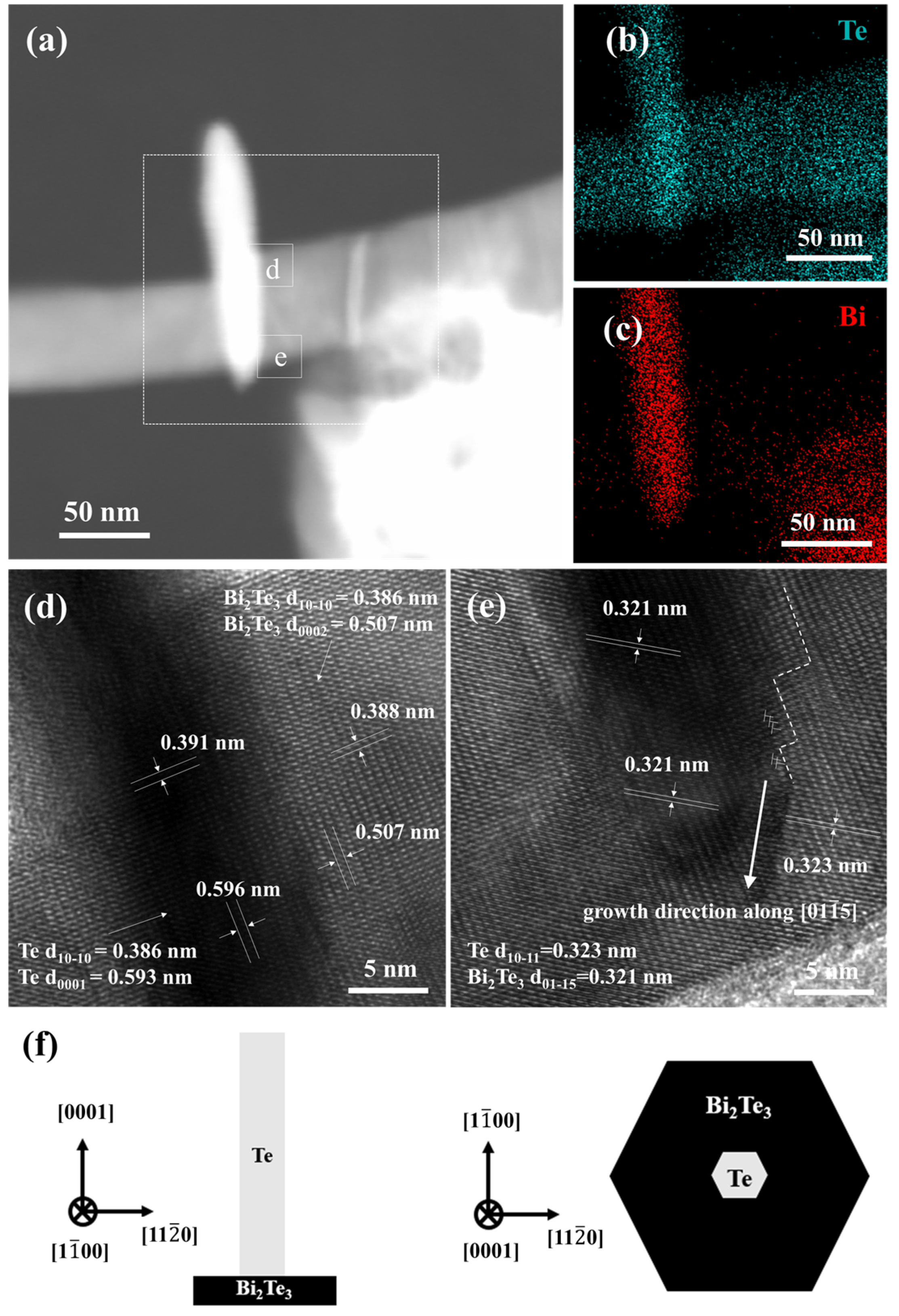
To further understand the predicted growth mechanism of the Bi2Te3 nanosheets, a Bi2Te3-Te hierarchical nanostructure was observed directly under TEM, as shown in Figure 7. In Figure 7a, the appearance of the Bi2Te3-Te heterostructure is observed under the above parameters. The EDS analysis for elemental mapping in HAADF-STEM images (Figure 7b,c) can further confirm that the composition of the nanowire is ultra-pure Te, and the Bi/Te ratio of the nanosheets (white square) is close to the chemical dose ratio of Bi2Te3. The early stage of the Bi2Te3 nanosheets undergoes oriented attachment, while the Te atoms continue to diffuse to the surface, reacting with the Bi precursor and shortening the length of the Te nanowires.

Figure 7.
(a) HAADF-STEM image of the Bi2Te3-Te hierarchical heterostructure synthesized at 170 °C for 1 h in 0.3 M NaOH. EDS elemental mapping results of (b) Te and (c) Bi. (d,e) HRTEM images of the squares representing Regions d and e in (a), respectively. (f) Schematic diagram showing the crystal orientation of the Bi2Te3-Te hierarchical heterostructure.
Furthermore, the HRTEM images of the white square representing Region d in Figure 7d show that the interplanar distances are calculated to be approximately 0.391 nm and 0.596 nm, which are nearly consistent with the literature values of the Te (10) and (0001) planes, respectively [28]. The interplanar distances are calculated to be approximately 0.388 nm and 0.507 nm, which are also consistent with the reported values of the Bi2Te3 (10) and (0002) planes, respectively [28]. Additionally, the lattice relationship in the HRTEM images of the white square representing Region e, as shown in Figure 7e, is investigated, and the interplanar distances are calculated to be approximately 0.323 nm and 0.321 nm, which are nearly consistent with those of the Te (10) and Bi2Te3 (01) planes, respectively. It is also worth noting that a very high density of dislocations accumulates at the Bi2Te3-Te interface; therefore, the growth direction of Bi2Te3 nanosheets advances in a zigzag shape along with the [01] direction. The bent edge of the Bi2Te3 nanosheets becomes straight to reduce the surface energy, resulting in the formation of the {100} edge. In addition, the crystal orientation relationship between the hierarchical Bi2Te3-Te heterojunction atoms is illustrated in Figure 7f. It can be understood that the (0001) Te || (0002) Bi2Te3 and [11] Te || [11] Bi2Te3 [28]. Finally, a clearly outlined Bi2Te3 nanosheet form is successfully obtained at a late stage of the process.
4. Conclusions
In summary, the detailed growth mechanism of Bi2Te3 by using a simple one-pot solvothermal method is thoroughly understood. Several steps were sequentially observed in the solution. Te ion was first reduced by the hydroxide group to form Te nanowires by self-assembly. Second, Bi precursors adhered to the Te nanowires and reacted into hierarchical Te-Bi2Te3 nanostructured materials. Third, the Te atoms continuously diffused from the Te nanowire to the Bi-Te interface, providing the Te required for nanosheet growth and shortening the Te nanowire. Finally, the perfect morphological features of the Bi2Te3 nanosheets were successfully formed.
In addition, a higher alkaline concentration and lower reaction temperature resulted in wider and thinner Bi2Te3 nanosheets, as shown in the AFM statistical analysis. With increasing base concentration, more hydroxide ions act as reducing agents, leading to an increase in the yield of Bi2Te3 nanosheets with perfect morphology. As for increasing reaction temperature or time, it increases the motion of ions in solution in in-plane and out-of-plane directions and the diffusion of Te atoms into the Te nanowires, resulting in a little thicker Bi2Te3 nanosheets. The higher NaOH concentration simultaneously leads to faster growth along the out-of-plane direction, resulting in a larger size and thinner Bi2Te3 nanosheets.
On the other hand, the use of UV–Vis–NIR spectroscopy is helpful to rapidly understand the morphological evolution of Bi2Te3 nanosheets in solution. The main broad peak on the spectrum tended to be red-shifted, while the other sharp peak in the ultraviolet range weakened during the synthesis of Bi2Te3 nanosheets. By rationalizing the above series of observations, we report for the first time that environmental SEM, TEM, and UV–Vis–NIR spectroscopy successfully confirm the growth mechanism of Bi2Te3 nanosheet through the liquid–solid formation. This research constructively provides an optimized process for Bi2Te3 nanosheets, which shows promising applications as thermoelectrics, topological insulators, and nanogenerators in future micro and nanoelectronic devices.
Supplementary Materials
The following supporting information can be downloaded at: https://www.mdpi.com/article/10.3390/nano12132236/s1, Figure S1. SEM images of the hexagonal Bi2Te3 nanosheets synthesized in (a) 0.2 M, (b) 0.3 M, (c) 0.4 M, and (d) 0.5 M NaOH at 190 °C for 1 h. The hexagonal Bi2Te3 nanosheets synthesized in (e) 0.2 M, (f) 0.3 M, (g) 0.4 M, and (h) 0.5 M NaOH at 190 °C for 3 h. Figure S2: The histograms of size distributions of Bi2Te3 nanosheets from Figure 3a,b. Figure S3: The histograms of thickness distributions of Bi2Te3 nanosheets from Figure 3a,b. Figure S4. SEM images of the changes in the morphology of the hexagonal Bi2Te3 nanosheets synthesized in 0.4 M NaOH at 170 °C for different reaction times: (a) 3 min, (b) 5 min, (c) 10 min, (d) 15 min, (e) 20 min, and (f) 30 min. The scale bar in the figure is 1 micrometer, and the scale bar in the inset figure is 400 nanometers. Figure S5. SEM images of the changes in the morphology of the hexagonal Bi2Te3 nanosheets synthesized in 0.4 M NaOH at 190 °C for different reaction times: (a) 3 min, (b) 5 min, (c) 10 min, (d) 15 min, (e) 20 min, and (f) 30 min. The scale bar in the figure is 1 micrometer, and the scale bar in the inset figure is 400 nanometers.
Author Contributions
Conceptualization, C.-Y.C.; methodology, C.-Y.C., R.-P.L., S.-Y.L. and Y.-J.L.; software, R.-P.L. and S.-Y.L.; validation, R.-P.L., S.-Y.L. and Y.-J.L.; Visualization, S.-Y.L., Y.-J.L. and C.-Y.C.; formal analysis, R.-P.L. and S.-Y.L.; investigation, R.-P.L. and S.-Y.L. and C.-Y.C.; resources, C.-Y.C.; data curation, R.-P.L., S.-Y.L. and C.-Y.C.; writing—original draft preparation, R.-P.L. and C.-Y.C.; writing—review and editing, C.-Y.C.; project administration, C.-Y.C.; funding acquisition, C.-Y.C. All authors have read and agreed to the published version of the manuscript.
Funding
This work was funded by the Ministry of Science and Technology (MOST), Taiwan, and the foundation grant MOST 107-2112-M-110-013-MY3 and MOST 110-2112-M-110-017-MY2.
Institutional Review Board Statement
Not applicable.
Informed Consent Statement
Not applicable.
Data Availability Statement
Data presented in this article are available at request from the corresponding author.
Acknowledgments
We appreciate the support for analysis from the Precision Instrument Center of National Sun Yat-sen University (NSYSU) in Taiwan. We thank Wen-Shuo Chuang for his assistance and helpful discussions. This research was also supported in part by FlowVIEW Tek.
Conflicts of Interest
The authors declare no conflict of interest.
References
- Chen, Y.L.; Analytis, J.G.; Chu, J.-H.; Liu, Z.K.; Mo, S.-K.; Qi, X.L.; Zhang, H.J.; Lu, D.H.; Dai, X.; Fang, Z.; et al. Experimental Realization of a Three-Dimensional Topological Insulator, Bi2Te3. Science 2009, 325, 178–181. [Google Scholar] [CrossRef] [PubMed] [Green Version]
- Hsieh, D.; Xia, Y.; Qian, D.; Wray, L.; Meier, F.; Dil, J.H.; Osterwalder, J.; Patthey, L.; Fedorov, A.V.; Lin, H.; et al. Observation of time-reversal-protected single-dirac-cone topological-insulator states in Bi2Te3 and Sb2Te3. Phys. Rev. Lett. 2009, 103, 146401. [Google Scholar] [CrossRef] [PubMed] [Green Version]
- Peng, H.; Dang, W.; Cao, J.; Chen, Y.; Wu, D.; Zheng, W.; Li, H.; Shen, Z.-X.; Liu, Z. Topological insulator nanostructures for near-infrared transparent flexible electrodes. Nat. Chem. 2012, 4, 281–286. [Google Scholar] [CrossRef] [PubMed]
- Qiao, H.; Yuan, J.; Xu, Z.; Chen, C.; Lin, S.; Wang, Y.; Song, J.; Liu, Y.; Khan, Q.; Hoh, H.Y.; et al. Broadband Photodetectors Based on Graphene–Bi2Te3 Heterostructure. ACS Nano 2015, 9, 1886–1894. [Google Scholar] [CrossRef] [PubMed]
- Yao, J.; Zheng, Z.; Yang, G. All-Layered 2D Optoelectronics: A High-Performance UV–vis–NIR Broadband SnSe Photodetector with Bi2Te3 Topological Insulator Electrodes. Adv. Funct. Mater. 2017, 27, 1701823. [Google Scholar] [CrossRef]
- Zhang, H.; Zhang, X.; Liu, C.; Lee, S.-T.; Jie, J. High-Responsivity, High-Detectivity, Ultrafast Topological Insulator Bi2Se3 /Silicon Heterostructure Broadband Photodetectors. ACS Nano 2016, 10, 5113–5122. [Google Scholar] [CrossRef]
- Xu, N.; Xu, Y.; Zhu, J. Topological insulators for thermoelectrics. Npj Quantum. Mater. 2017, 2, 51. [Google Scholar] [CrossRef]
- Kong, D.; Zhu, W.; Guo, Z.; Deng, Y. High-performance flexible Bi2Te3 films based wearable thermoelectric generator for energy harvesting. Energy 2019, 175, 292–299. [Google Scholar] [CrossRef]
- Witting, I.T.; Chasapis, T.C.; Ricci, F.; Peters, M.; Heinz, N.A.; Hautier, G.; Snyder, G.J. The Thermoelectric Properties of Bismuth Telluride. Adv. Electron. Mater. 2019, 5, 1800904. [Google Scholar] [CrossRef]
- Li, M.; Lu, H.-W.; Wang, S.-W.; Li, R.-P.; Chen, J.-Y.; Chuang, W.-S.; Yang, F.-S.; Lin, Y.-F.; Chen, C.-Y.; Lai, Y.-C. Filling the gap between topological insulator nanomaterials and triboelectric nanogenerators. Nat. Commun. 2022, 13, 938. [Google Scholar] [CrossRef]
- Huang, B.-L.; Kaviany, M. Ab initio and molecular dynamics predictions for electron and phonon transport in bismuth telluride. Phys. Rev. B 2008, 77, 125209. [Google Scholar] [CrossRef] [Green Version]
- Hosokawa, Y.; Tomita, K.; Takashiri, M. Growth of single-crystalline Bi2Te3 hexagonal nanoplates with and without single nanopores during temperature-controlled solvothermal synthesis. Sci. Rep. 2019, 9, 10790. [Google Scholar] [CrossRef] [PubMed] [Green Version]
- Yang, M.; Wang, J.; Zhao, Y.; He, L.; Ji, C.; Liu, X.; Zhou, H.; Wu, Z.; Wang, X.; Jiang, Y. Three-Dimensional Topological Insulator Bi2Te3/Organic Thin Film Heterojunction Photodetector with Fast and Wideband Response from 450 to 3500 Nanometers. ACS Nano 2019, 13, 755–763. [Google Scholar] [CrossRef]
- Bulman, G.; Barletta, P.; Lewis, J.; Baldasaro, N.; Manno, M.; Bar-Cohen, A.; Yang, B. Superlattice-based thin-film thermoelectric modules with high cooling fluxes. Nat. Commun. 2016, 7, 10302. [Google Scholar] [CrossRef]
- Liu, J.; Wang, H.; Li, X.; Chen, H.; Zhang, Z.; Pan, W.; Luo, G.; Yuan, C.; Ren, Y.; Lei, W. High performance visible photodetectors based on thin two-dimensional Bi2Te3 nanoplates. J. Alloys Compd. 2019, 798, 656–664. [Google Scholar] [CrossRef]
- Wei, Q.; Niu, K.; Han, X.; Zhang, H.; Zhang, C.; Yang, C.; Man, B. Large energy pulses generation in a mode-locked Er-doped fiber laser based on CVD-grown Bi2Te3 saturable absorber. Opt. Mater. Express 2019, 9, 3535–3545. [Google Scholar] [CrossRef]
- Krumrain, J.; Mussler, G.; Borisova, S.; Stoica, T.; Plucinski, L.; Schneider, C.; Grützmacher, D. MBE growth optimization of topological insulator Bi2Te3 films. J. Cryst. Growth 2011, 324, 115–118. [Google Scholar] [CrossRef]
- Zeng, Z.; Morgan, T.; Fan, D.; Li, C.; Hirono, Y.; Hu, X.; Zhao, Y.; Lee, J.S.; Wang, J.; Wang, Z.M.; et al. Molecular beam epitaxial growth of Bi2Te3 and Sb2Te3 topological insulators on GaAs (111) substrates: A potential route to fabricate topological insulator p-n junction. AIP Adv. 2013, 3, 072112. [Google Scholar] [CrossRef]
- Lin, Z.; Chen, Y.; Yin, A.; He, Q.; Huang, X.; Xu, Y.; Liu, Y.; Zhong, X.; Huang, Y.; Duan, X. Solution Processable Colloidal Nanoplates as Building Blocks for High-Performance Electronic Thin Films on Flexible Substrates. Nano Lett. 2014, 14, 6547–6553. [Google Scholar] [CrossRef]
- Zhao, M.; Bosman, M.; Danesh, M.; Zeng, M.; Song, P.; Darma, Y.; Rusydi, A.; Lin, H.; Qiu, C.-W.; Loh, K.P. Visible Surface Plasmon Modes in Single Bi2Te3 Nanoplate. Nano Lett. 2015, 15, 8331–8335. [Google Scholar] [CrossRef]
- Liu, Y.; Wang, Q.; Pan, J.; Sun, Y.; Zhang, L.; Song, S. Hierarchical Bi2Te3 Nanostrings: Green Synthesis and Their Thermoelectric Properties. Chem.–A Eur. J. 2018, 24, 9765–9768. [Google Scholar] [CrossRef] [PubMed]
- Park, G.; Lee, J.; Moon, S.; Yang, H.; Giri, A.; Kwak, J.; Jung, Y.-K.; Soon, A.; Jeong, U. Eventual Chemical Transformation of Metals and Chalcogens into Metal Chalcogenide Nanoplates through a Surface Nucleation-Detachment-Reorganization Mechanism. Chem. Mater. 2017, 29, 3219–3227. [Google Scholar] [CrossRef]
- Mi, J.-L.; Lock, N.; Sun, T.; Christensen, M.; Søndergaard, M.; Hald, P.; Hng, H.H.; Ma, J.; Iversen, B.B. Biomolecule-Assisted Hydrothermal Synthesis and Self-Assembly of Bi2Te3 Nanostring-Cluster Hierarchical Structure. ACS Nano 2010, 4, 2523–2530. [Google Scholar] [CrossRef] [PubMed]
- Sharifi, T.; Yazdi, S.; Costin, G.; Apte, A.; Coulter, G.; Tiwary, C.; Ajayan, P.M. Impurity-Controlled Crystal Growth in Low-Dimensional Bismuth Telluride. Chem. Mater. 2018, 30, 6108–6115. [Google Scholar] [CrossRef]
- Lin, Z.-H.; Yang, Z.; Chang, H.-T. Preparation of Fluorescent Tellurium Nanowires at Room Temperature. Cryst. Growth Des. 2007, 8, 351–357. [Google Scholar] [CrossRef]
- Zhao, M.; Zhang, J.; Gao, N.; Song, P.; Bosman, M.; Peng, B.; Sun, B.; Qiu, C.-W.; Xu, Q.-H.; Bao, Q.; et al. Actively Tunable Visible Surface Plasmons in Bi2Te3 and their Energy-Harvesting Applications. Adv. Mater. 2016, 28, 3138–3144. [Google Scholar] [CrossRef]
- Dun, C.; Hewitt, C.A.; Jiang, Q.; Guo, Y.; Xu, J.; Li, Y.; Li, Q.; Wang, H.; Carroll, D.L. Bi2Te3 Plates with Single Nanopore: The Formation of Surface Defects and Self-Repair Growth. Chem. Mater. 2018, 30, 1965–1970. [Google Scholar] [CrossRef]
- Liu, S.; Li, H.; Han, W.; Sun, J.; Chen, G.; Chen, J.; Yang, X.; Chen, G.; Ma, F. Realizing the Interface Tuned Thermoelectric Transport Performance in Bi2Te3-Based Hierarchical Nanostructures. J. Phys. Chem. C 2019, 123, 23817–23825. [Google Scholar] [CrossRef]


Publisher’s Note: MDPI stays neutral with regard to jurisdictional claims in published maps and institutional affiliations. |
© 2022 by the authors. Licensee MDPI, Basel, Switzerland. This article is an open access article distributed under the terms and conditions of the Creative Commons Attribution (CC BY) license (https://creativecommons.org/licenses/by/4.0/).