Optical Sensitivity of Waveguides Inscribed in Nanoporous Silicate Framework


 ,
, 
Abstract
1. Introduction
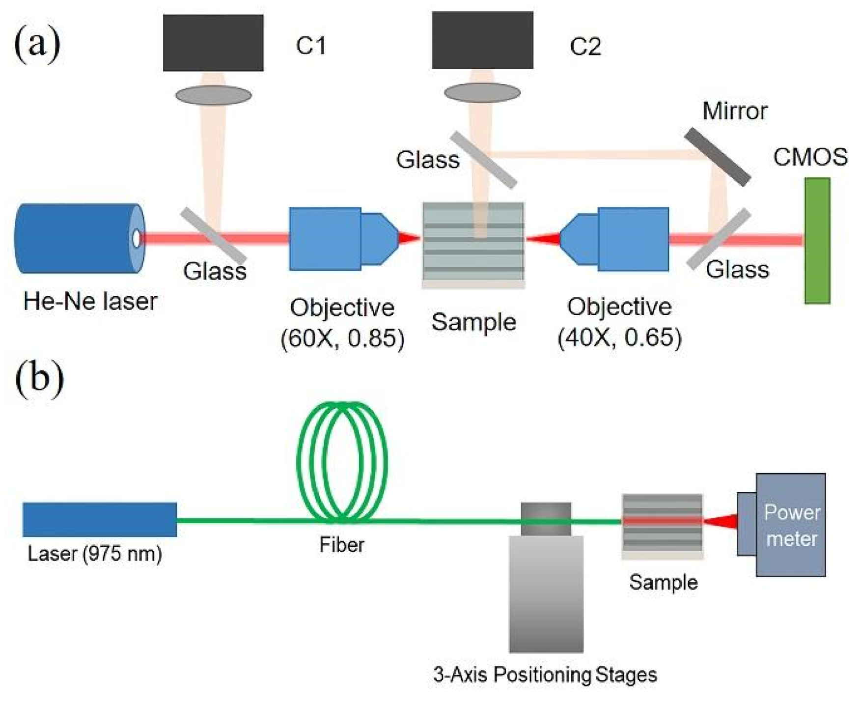
2. Experiments
2.1. LDW of Waveguides in PG
2.2. Waveguides Testing
3. Results and Discussion
3.1. Waveguide Fabrication
3.2. Thermal Resistance of Waveguides
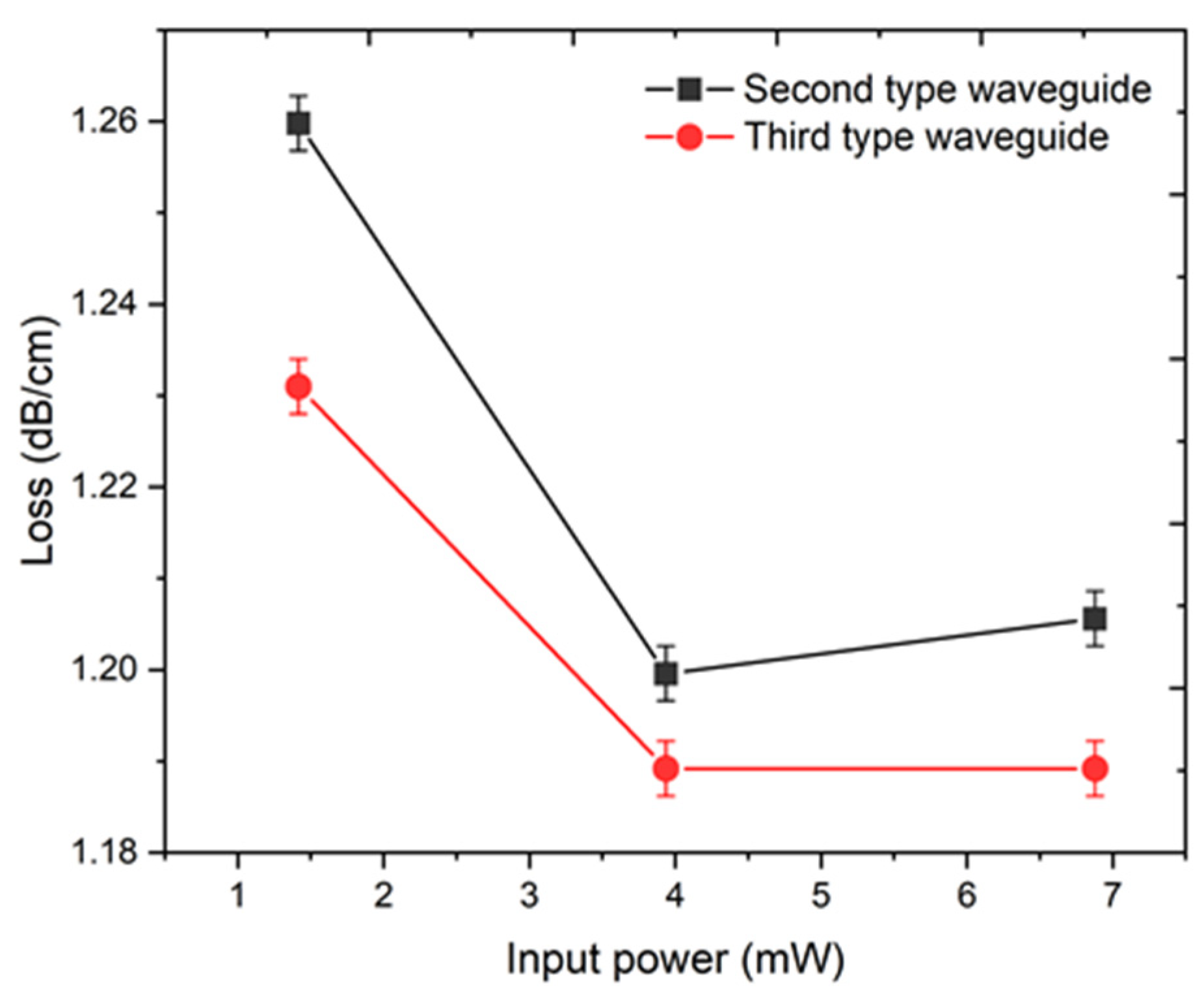
3.3. Waveguide Properties: Types, Refractive Index Profile, and Losses
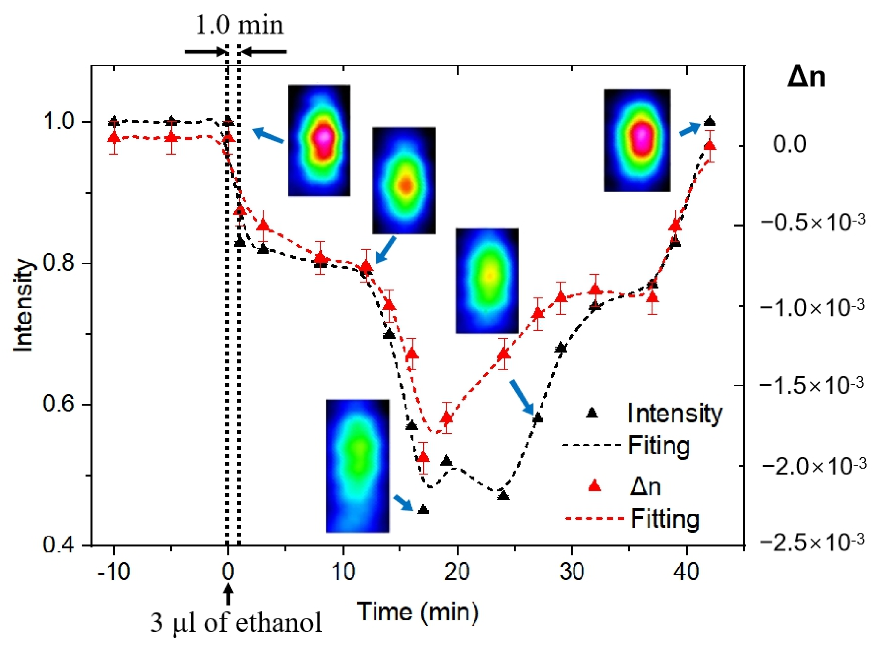
3.4. Opto-Fluidic Waveguide for Ethanol Molecule Sensing
4. Conclusions
Author Contributions
Funding
Institutional Review Board Statement
Informed Consent Statement
Data Availability Statement
Acknowledgments
Conflicts of Interest
References
- Nordberg, M.E. Properties of some Vycor-brand glasses. J. Am. Ceram. Soc. 1944, 27, 299–305. [Google Scholar] [CrossRef]
- Enke, D.; Janowski, F.; Schwieger, W. Porous glasses in the 21st century––A short review. Microporous Mesoporous Mater. 2003, 60, 19–30. [Google Scholar] [CrossRef]
- Maruo, Y.Y.; Nakamura, J. Portable formaldehyde monitoring device using porous glass sensor and its applications in indoor air quality studies. Anal. Chim. Acta 2011, 702, 247–253. [Google Scholar] [CrossRef] [PubMed]
- Izumi, K.; Utiyama, M.; Maruo, Y.Y. Colorimetric NOx sensor based on a porous glass-based NO2 sensing chip and a permanganate oxidizer. Sens. Actuators B Chem. 2015, 216, 128–133. [Google Scholar] [CrossRef]
- Izumi, K.; Utiyama, M.; Maruo, Y.Y. A porous glass-based ozone sensing chip impregnated with potassium iodide and α-cyclodextrin. Sens. Actuators B Chem. 2017, 241, 116–122. [Google Scholar] [CrossRef]
- Maruo, Y.Y.; Tachibana, K.; Suzuki, Y.; Shinomi, K. Development of an analytical chip for detecting acetone using a reaction between acetone and 2, 4-dinitrophenylhidrazine in a porous glass. Microchem. J. 2018, 141, 377–381. [Google Scholar] [CrossRef]
- Shakhgil’dyan, G.Y.; Piyanzina, K.I.; Stepko, A.A.; Natyrov, A.N.; Mikhailov, A.M.; Savinkov, V.I.; Sigaev, V.N. Nanoporous Glass with Controlled Pore Size for High-Efficiency Synthesis of Oligonucleotides. Glass Ceram. 2019, 75, 377–382. [Google Scholar] [CrossRef]
- Veiko, V.P.; Zakoldaev, R.A.; Sergeev, M.M.; Danilov, P.A.; Kudryashov, S.I.; Kostiuk, G.K.; Sivers, A.N.; Ionin, A.A.; Antropova, T.V.; Medvedev, O.S. Direct laser writing of barriers with controllable permeability in porous glass. Opt. Express 2018, 26, 28150–28160. [Google Scholar] [CrossRef]
- Rong, G.; Najmaie, A.; Sipe, J.E.; Weiss, S.M. Nanoscale porous silicon waveguide for label-free DNA sensing. Biosens. Bioelectron. 2008, 23, 1572–1576. [Google Scholar] [CrossRef]
- Gooding, J.J.; Gaus, K. Single-Molecule Sensors: Challenges and Opportunities for Quantitative Analysis. Angew. Chem. Int. Ed. 2016, 55, 11354–11366. [Google Scholar] [CrossRef]
- Cao, C.; Long, Y.-T. Biological Nanopores: Confined Spaces for Electrochemical Single-Molecule Analysis. Acc. Chem. Res. 2018, 51, 331–341. [Google Scholar] [CrossRef] [PubMed]
- Meng, F.-N.; Ying, Y.-L.; Yang, J.; Long, Y.-T. A Wild-Type Nanopore Sensor for Protein Kinase Activity. Anal. Chem. 2019, 91, 9910–9915. [Google Scholar] [CrossRef] [PubMed]
- Fukumori, Y.; Takada, K.; Takeuchi, H. Nanoporous and nanosize materials for drug delivery systems. In Nanomaterials for Medical Diagnosis and Therapy; Wiley-VCH Verlag GmbH&Co. KGaA: Weinheim, Germany, 2007; pp. 255–309. [Google Scholar] [CrossRef]
- Wang, Y.; Zhao, Q.; Hu, Y.; Sun, L.; Bai, L.; Jiang, T.; Wang, S. Ordered nanoporous silica as carriers for improved delivery of water insoluble drugs: A comparative study between three dimensional and two dimensional macroporous silica. Int. J. Nanomed. 2013, 8, 4015. [Google Scholar] [CrossRef] [PubMed]
- Wang, X.; Yu, H.; Li, P.; Zhang, Y.; Wen, Y.; Qiu, Y.; Liu, Z.; Li, Y.; Liu, L. Femtosecond laser-based processing methods and their applications in optical device manufacturing: A review. Opt. Laser Technol. 2021, 135, 106687. [Google Scholar] [CrossRef]
- Gattass, R.R.; Mazur, E. Femtosecond laser micromachining in transparent materials. Nat. Photonics 2008, 2, 219–225. [Google Scholar] [CrossRef]
- Choudhury, D.; Macdonald, J.R.; Kar, A.K. Ultrafast laser inscription: Perspectives on future integrated applications. Laser Photonics Rev. 2014, 8, 827–846. [Google Scholar] [CrossRef]
- Pitsios, I.; Samara, F.; Corrielli, G.; Crespi, A.; Osellame, R. Geometrically-controlled polarisation processing in femtosecond-laser-written photonic circuits. Sci. Rep. 2017, 7, 1–10. [Google Scholar] [CrossRef]
- Hoyo, J.; Berdejo, V.; Toney Fernandez, T.; Ferrer, A.; Ruiz, A.; Valles, J.A.; Rebolledo, M.A.; Ortega-Feliu, I.; Solis, J. Femtosecond laser written 16.5 mm long glass-waveguide amplifier and laser with 5.2 dB cm−1 internal gain at 1534 nm. Laser Phys. Lett. 2013, 10, 105802. [Google Scholar] [CrossRef]
- Crespi, A.; Gu, Y.; Ngamsom, B.; Hoekstra, H.J.; Dongre, C.; Pollnau, M.; Ramponi, R.; van den Vlekkert, H.H.; Watts, P.; Cerullo, G. Three-dimensional Mach-Zehnder interferometer in a microfluidic chip for spatially-resolved label-free detection. Lab. A Chip. 2010, 10, 1167–1173. [Google Scholar] [CrossRef]
- Lapointe, J.; Parent, F.; de Lima Filho, E.S.; Loranger, S.; Kashyap, R. Toward the integration of optical sensors in smartphone screens using femtosecond laser writing. Opt. Lett. 2015, 40, 5654–5657. [Google Scholar] [CrossRef]
- Nolte, S.; Will, M.; Burghoff, J.; Tuennermann, A. Femtosecond waveguide writing: A new avenue to three-dimensional integrated optics. Appl. Phys. A 2003, 77, 109–111. [Google Scholar] [CrossRef]
- Arriola, A.; Gross, S.; Jovanovic, N.; Charles, N.; Tuthill, P.G.; Olaizola, S.M.; Fuerbach, A.; Withford, M.J. Low bend loss waveguides enable compact, efficient 3D photonic chips. Opt. Express 2013, 21, 2978–2986. [Google Scholar] [CrossRef] [PubMed]
- Petit, Y.; Danto, S.; Guérineau, T.; Abou Khalil, A.; Le Camus, A.; Fargin, E.; Duchateau, G.; Bérubé, J.-P.; Vallée, R.; Messaddeq, Y.; et al. On the femtosecond laser-induced photochemistry in silver-containing oxide glasses: Mechanisms, related optical and physico-chemical properties, and technological applications. Adv. Opt. Technol. 2018, 7, 291–309. [Google Scholar] [CrossRef]
- Abou Khalil, A.; Bérubé, J.-P.; Danto, S.; Desmoulin, J.-C.; Cardinal, T.; Petit, Y.; Vallée, R.; Canioni, L. Direct laser writing of a new type of waveguides in silver containing glasses. Sci. Rep. 2017, 7, 11124. [Google Scholar] [CrossRef]
- Lapointe, J.; Gagné, M.; Li, M.-J.; Kashyap, R. Making smart phones smarter with photonics. Opt. Express 2014, 22, 15473–15483. [Google Scholar] [CrossRef]
- Meany, T.; Gräfe, M.; Heilmann, R.; Perez-Leija, A.; Gross, S.; Steel, M.J.; Withford, M.J.; Szameit, A. Laser written circuits for quantum photonics. Laser Photonics Rev. 2015, 9, 363–384. [Google Scholar] [CrossRef]
- Crespi, A.; Osellame, R.; Ramponi, R.; Brod, D.J.; Galvão, E.F.; Spagnolo, N.; Vitelli, C.; Maiorino, E.; Mataloni, P.; Sciarrino, F. Integrated multimode interferometers with arbitrary designs for photonic boson sampling. Nat. Photonics 2013, 7, 545–549. [Google Scholar] [CrossRef]
- Knill, E.; Laflamme, R.; Milburn, G.J. A scheme for efficient quantum computation with linear optics. Nature 2001, 409, 46–52. [Google Scholar] [CrossRef]
- Crespi, A.; Lobino, M.; Matthews, J.C.; Politi, A.; Neal, C.R.; Ramponi, R.; Osellame, R.; O’Brien, J.L. Measuring protein concentration with entangled photons. Appl. Phys. Lett. 2012, 100, 233704. [Google Scholar] [CrossRef]
- Lijing, Z.; Zakoldaev, R.A.; Sergeev, M.M.; Veiko, V.P. Fluorescent Bulk Waveguide Sensor in Porous Glass: Concept, Fabrication, and Testing. Nanomaterials 2020, 10, 2169. [Google Scholar] [CrossRef]
- Veiko, V.P.; Kudryashov, S.I.; Sergeev, M.M.; Zakoldaev, R.A.; Danilov, P.A.; Ionin, A.A.; Antropova, T.V.; Anfimova, I.N. Femtosecond laser-induced stress-free ultra-densification inside porous glass. Laser Phys. Lett. 2016, 13, 055901. [Google Scholar] [CrossRef]
- Itina, T.E.; Zakoldaev, R.A.; Sergeev, M.M.; Ma, H.; Kudryashov, S.I.; Medvedev, O.S.; Veiko, V.P. Ultra-short laser-induced high aspect ratio densification in porous glass. Opt. Mater. Express 2019, 9, 4379–4389. [Google Scholar] [CrossRef]
- Kreisberg, V.; Antropova, T.; Kalinina, S. Formation of micro-and mesoporous substructures in the course of the leaching process of two-phase alkali borosilicate glass. Glass Phys. Chem. 2014, 40, 384–387. [Google Scholar] [CrossRef]
- Zhong, L.; Zakoldaev, R.A.; Sergeev, M.M.; Veiko, V.P.; Li, Z. Porous glass density tailoring by femtosecond laser pulses. Opt. Quantum Electron. 2020, 52, 49. [Google Scholar] [CrossRef]
- Szameit, A.; Burghoff, J.; Pertsch, T.; Nolte, S.; Tünnermann, A.; Lederer, F. Two-dimensional soliton in cubic fs laser written waveguide arrays in fused silica. Opt. Express 2006, 14, 6055–6062. [Google Scholar] [CrossRef]
- Mansour, I.; Caccavale, F. An improved procedure to calculate the refractive index profile from the measured near-field intensity. J. Lightwave Technol. 1996, 14, 423–428. [Google Scholar] [CrossRef]
- Liao, Y.; Cheng, Y. Femtosecond Laser 3D Fabrication in Porous Glass for Micro-and Nanofluidic Applications. Micromachines 2014, 5, 1106–1134. [Google Scholar] [CrossRef]
- Nolte, S.; Will, M.; Burghoff, J.; Tünnermann, A. Ultrafast laser processing: New options for three-dimensional photonic structures. J. Mod. Opt. 2004, 51, 2533–2542. [Google Scholar] [CrossRef]
- Boisvert, J.-S.; Loranger, S.; Lorre, P.; Iezzi, V.L.; Kashyap, R. Effect of fs laser exposure on the strength of toughened multimedia glass. J. Non-Cryst. Solids 2019, 521, 119467. [Google Scholar] [CrossRef]
- Eaton, S.M.; Zhang, H.; Herman, P.R.; Yoshino, F.; Shah, L.; Bovatsek, J.; Arai, A.Y. Heat accumulation effects in femtosecond laser-written waveguides with variable repetition rate. Opt. Express 2005, 13, 4708–4716. [Google Scholar] [CrossRef]
- Couairon, A.; Mysyrowicz, A. Femtosecond filamentation in transparent media. Phys. Rep. 2007, 441, 47–189. [Google Scholar] [CrossRef]
- Shah, L.; Arai, A.Y.; Eaton, S.M.; Herman, P.R. Waveguide writing in fused silica with a femtosecond fiber laser at 522 nm and 1 MHz repetition rate. Opt. Express 2005, 13, 1999–2006. [Google Scholar] [CrossRef]
- Girault, P.; Azuelos, P.; Lorrain, N.; Poffo, L.; Lemaitre, J.; Pirasteh, P.; Hardy, I.; Thual, M.; Guendouz, M.; Charrier, J. Porous silicon micro-resonator implemented by standard photolithography process for sensing application. Opt. Mater. 2017, 72, 596–601. [Google Scholar] [CrossRef]
- Mathias, D. Ethanol—Small molecule, strong toxin. In Staying Healthy From 1 to 100: Diet and Exercise Current Medical Knowledge on How to Keep Healthy; Springer: Berlin/Heidelberg, Germany, 2016; p. 39. [Google Scholar] [CrossRef]
- Ishikawa, A.; Chiang, T.H.; Toda, F. Separation of water–alcohol mixtures by permeation through a zeolite membrane on porous glass. J. Chem. Soc. Chem. Commun. 1989, 764–765. [Google Scholar] [CrossRef]
- Tan, D.; Sun, X.; Wang, Q.; Zhou, P.; Liao, Y.; Qiu, J. Fabricating low loss waveguides over a large depth in glass by temperature gradient assisted femtosecond laser writing. Opt. Let. 2020, 45, 3941–3944. [Google Scholar] [CrossRef] [PubMed]
- Chen, G.Y.; Piantedosi, F.; Otten, D.; Kang, Y.Q.; Zhang, W.Q.; Zhou, X.; Monro, T.M.; Lancaster, D.G. Femtosecond-laser-written Microstructured Waveguides in BK7 Glass. Sci. Rep. 2018, 8, 10377. [Google Scholar] [CrossRef]
- Degen, C.L.; Reinhard, F.; Cappellaro, P. Quantum sensing. Rev. Mod. Phys. 2017, 89, 035002. [Google Scholar] [CrossRef]


Publisher’s Note: MDPI stays neutral with regard to jurisdictional claims in published maps and institutional affiliations. |
© 2021 by the authors. Licensee MDPI, Basel, Switzerland. This article is an open access article distributed under the terms and conditions of the Creative Commons Attribution (CC BY) license (http://creativecommons.org/licenses/by/4.0/).
Share and Cite
Lijing, Z.; Zakoldaev, R.A.; Sergeev, M.M.; Petrov, A.B.; Veiko, V.P.; Alodjants, A.P. Optical Sensitivity of Waveguides Inscribed in Nanoporous Silicate Framework. Nanomaterials 2021, 11, 123. https://doi.org/10.3390/nano11010123
Lijing Z, Zakoldaev RA, Sergeev MM, Petrov AB, Veiko VP, Alodjants AP. Optical Sensitivity of Waveguides Inscribed in Nanoporous Silicate Framework. Nanomaterials. 2021; 11(1):123. https://doi.org/10.3390/nano11010123
Chicago/Turabian StyleLijing, Zhong, Roman A. Zakoldaev, Maksim M. Sergeev, Andrey B. Petrov, Vadim P. Veiko, and Alexander P. Alodjants. 2021. "Optical Sensitivity of Waveguides Inscribed in Nanoporous Silicate Framework" Nanomaterials 11, no. 1: 123. https://doi.org/10.3390/nano11010123
APA StyleLijing, Z., Zakoldaev, R. A., Sergeev, M. M., Petrov, A. B., Veiko, V. P., & Alodjants, A. P. (2021). Optical Sensitivity of Waveguides Inscribed in Nanoporous Silicate Framework. Nanomaterials, 11(1), 123. https://doi.org/10.3390/nano11010123