Article

Impact of Photo-Excitation on Leakage Current and Negative Bias Instability in InSnZnO Thickness-Varied Thin-Film Transistors

1
Key Laboratory of Applied Surface and Colloid Chemistry, Ministry of Education, Shaanxi Normal University, Xian 710119, China
2
Shaanxi Key Laboratory for Advanced Energy Devices; Shaanxi Engineering Lab for Advanced Energy Technology, Shaanxi Normal University, Xian 710119, China
3
School of Materials Science and Engineering, Shaanxi Normal University, Xian 710119, China
4
School of Environmental Science and Engineering, Kochi University of Technology, Kami, Kochi 782-8502, Japan
5
Center for Nanotechnology in Research Institute, Kochi University of Technology, Kami, Kochi 782-8502, Japan
6
Advanced Technology Research Laboratories, Idemitsu Kosan Co. Ltd., Sodegaura, Chiba 299-0293, Japan
*
Authors to whom correspondence should be addressed.
Nanomaterials 2020, 10(9), 1782; https://doi.org/10.3390/nano10091782
Submission received: 13 August 2020 / Revised: 4 September 2020 / Accepted: 6 September 2020 / Published: 9 September 2020

Abstract

:
InSnZnO thin-film transistors (ITZO TFTs), having high carrier mobility, guarantee the benefits of potential applications in the next generation of super-high-definition flat-panel displays. However, the impact of photo-excitation on the leakage current and negative bias stress (NBIS) of ITZO TFTs must be further explored. In this study, the ITZO thickness (TITZO) is designed to tailor the initial performance of devices, especially for the 100 nm TITZO TFT, producing excellent electrical properties of 44.26 cm2V−1s−1 mobility, 92 mV/dec. subthreshold swing (SS), 0.04 V hysteresis, and 3.93 × 10¹⁰ ON/OFF ratio, which are superior to those of the reported ITZO TFTs. In addition, incident light coupled with tunable photon energy is introduced to monitor the leakage current of various TITZO devices. The OFF-current results demonstrate that under the identical photon energy, many more electrons are photo-excited for the thicker TITZO TFTs. NBIS-induced Vth shift and SS deterioration in all TFTs are traced and analyzed in real time. As the TITZO thickens to near Debye length, the degree of degradation is exacerbated. When the thickness further increases, the notorious instability caused by NBIS is effectively suppressed. This study provides an important research basis for the application of ITZO-based TFTs in future displays.

Graphical Abstract

1. Introduction

In the last two decades, thin-film transistors (TFTs) based on metal oxide semiconductors are one of encouraging low-input voltage electronic devices in transparent and flexible flat panel display (FPD) applications where traditional silicon-related TFTs are hard to match [1,2,3]. Among various metal oxide active layers, amorphous InGaZnO (a-IGZO)-dependent transistors have rapidly developed because they easily achieve high mobility (μ) of ~10 cm2V−1s−1 and long-term stability through creative approaches [4,5,6], including interface modification, doping engineering, and device structure adjustment. Nevertheless, their mobility is insufficient to satisfy the requirement of driving integrated circuits in ultra- and super-high-definition FPDs.
Due to the efforts of researchers, ternary and quaternary metal oxide semiconductors with different elements that regulate concentration have been designed in the pattern of permutation and combination. InSnZnO (ITZO), as an alternative candidate to active layers, can effectively contribute to a high μ of ~30 cm2V−1s−1 [7]. Simultaneously, other electrical parameters, including threshold voltage (Vth) and subthreshold swing (SS), have also been substantially improved in comparison with those of a-IGZO TFTs. The possible reasons for enhancing the μ of ITZO-based TFTs are commonly attributed to two scenarios. One scenario is where the atomic radius of Sn is 1.40 Å, which is larger than that of Ga (1.26 Å). As a consequence, the average distance between the Sn atom and its adjacent In atoms in the ITZO lattice is shorter than that between Ga and In atoms in the IGZO lattice with the identical element content [8]. In addition, increasing the overlap probability of Sn 5s and In 5s atomic orbitals is beneficial because it raises the μ along the conduction band (EC). The other is because the electron effective mass in the ITZO system is slightly lighter than that in a-IGZO [8], contributing to the increase in field-effect mobility.
Although much research has been devoted to the development of metal oxide TFTs, device stability is still an issue, particularly under the photo-excitation conditions, which restrict the process of industrialization. In terms of a-IGZO materials, despite incident light energy being lower than the band gap of a-IGZO [9], leakage of current is still observed and defects can be found. Moreover, new defect states are created in the IGZO bulk, even along the contacted interfaces. However, the photo-assisted negative bias stress (NBIS)-caused performance deterioration can be effectively avoided via test intervention [10], anion introduction [11], and treatment temperature regulation [12,13]. On the other hand, the NBIS-resulting Vth shift and SS degradation can be quantitatively analyzed by designing the oxide semiconductor thickness. In previous studies [14], we explored the dark state stabilities under test temperatures and drain current stress in a-ITZO TFTs. We therefore investigated how the ITZO thickness influences photo-excitation on leakage current and negative bias instability in the corresponding TFTs.
In this regard, we first examined how ITZO TFTs with different thickness (TITZO) are prepared. The electrical parameters of transfer curves for all devices were extracted and compared with the published ITZO-based TFT performance. We found that the electrical characteristics obtained in this study are generally superior to others. More importantly, the impacts of photo-excited OFF-current increase and NBIS-provoked instability in TITZO-varied TFTs were systematically investigated.

2. Experimental Methods

To construct the ITZO TFTs with various TITZO, the glass substrate was ultrasonically treated with acetone, isopropyl alcohol, and deionized water for 5 min, separately. The chromium film was fabricated on the treated glass and was dry etched to form the bottom electrode. The 150 nm thick SiO2 gate insulator was then using utilizing plasma-enhanced chemical vapor deposition (PECVD). In the case of the active layers, DC magnetron sputtering technology was adopted. The sputtering parameters, which included a deposition power of 60 W, operation pressure of 1 Pa, working gases of Ar and O2 with ratio of 15/15 sccm, and sputtering temperature of 30 °C, were fixed. In addition, the deposition duration was adjusted. Consequently, the ITZO films with the TITZO of 25, 45, 75, and 100 nm were tailored. After the pattern process, the geometric factor of length–width ratio was 20:50 μm as a result of the identical design specification. The SiO2 film (200 nm) was deposited again using PECVD to form an etch-stopper layer. The ITO source and drain electrodes were sequentially fabricated with the help of the sputtering method and etching technology. The SiO2 passivation layer was finally deposited to obtain bottom-gate top-contact ITZO TFTs. Subsequently, the devices were thermally heated in N2 at 350 °C for 1 h. In addition, the photo-excitation OFF-current results were investigated under illumination at wavelengths in the region of 400–530 nm. With regard to the operation conditions of NBIS evaluation, the wavelength, gate voltage, and stress duration were 460 nm, −20 V, and 104 s, respectively. The current–voltage (I–V) response was measured using an Agilent 4156C semiconductor parameter analyzer.

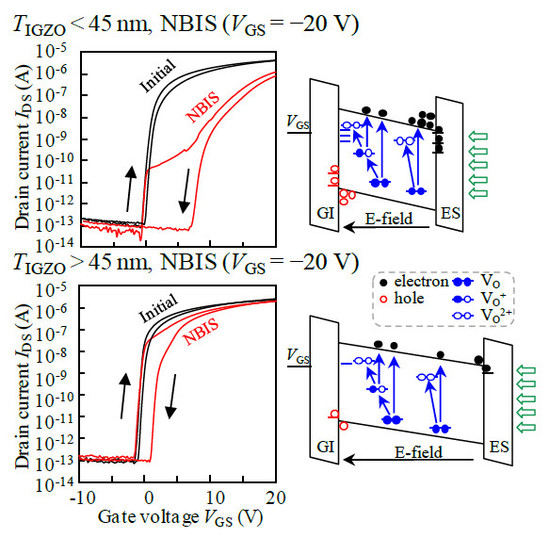
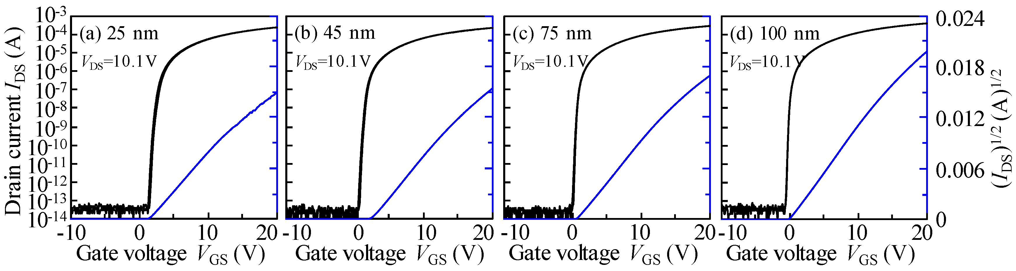
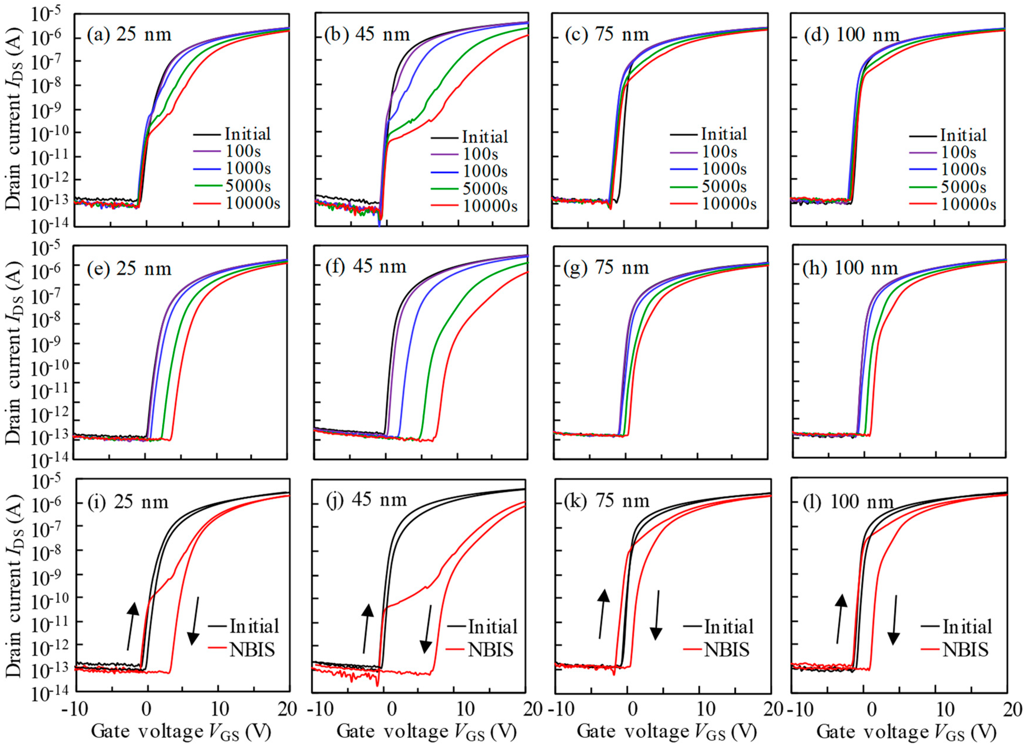
3. Results and Discussion

Figure 1 displays the transfer properties of ITZO thickness-varied TFTs measured at VDS = 10.1 V. The corresponding electrical parameters calculated from the forward scan are listed in Table 1. With respect to the TFT with 25 nm TITZO, outstanding electrical properties were observed: μsat of 34.73 cm2V−1s−1, Vth of 1.95 V, ON/OFF ratio of 2.38 × 10¹⁰, hysteresis ΔVH of 0.17 V, and SS of 206 mV/dec. When the TITZO increased to 45 nm and continued to thicken to 100 nm, the μsat slightly increased to 37.61 cm2V−1s−1, and gradually changed to 44.26 cm2V−1s−1. Additionally, as the TITZO increased, the ID rose. Considering the relationship between ID and μsat [15], the improvement in the μsat contributed to the increase in the ON current. The Vth negatively changed to 1.13 and −0.25 V, which correspond to 45 and 100 nm TITZO devices, respectively, as a result of the increase free carrier concentration in the thicker TITZO. The ON/OFF ratio reached more than 10 orders of magnitude and the hysteresis is almost negligible irrespective of the TITZO. The SS of 92 mV/dec. was obtained when the TITZO thickened to 100 nm. The SS value is a standard criterion of the total defect densities in the active layer and its adjacent interfaces [16]. This value suggests that high quality ITZO layer and front- and back-interfaces were designed in this work. Furthermore, compared with the performance of reviewed ITZO TFTs [17,18,19,20,21,22,23], as tabulated in Table 2, the 100 nm TITZO device in this study is superior.
The typical transfer curves of ITZO-varied devices were recorded from ON- to OFF-current direction under the external light exposure and VDS bias of 20.1 V, as described in Figure 2a–d. In general, the OFF-current is dependent on the incident photon energy and the TITZO, as summarized in Figure 2e. For the 25 nm TITZO TFT, when the incident light energy was greater than 2.70 eV, the photo-excited OFF-current slightly increased. This increase depends on the photon energy of incident light. As the TITZO s increased to 45 nm, high OFF-current was obtained, even under the identical photon energy of 2.70 eV. When the TITZO was further thickened to 75 and 100 nm, the photon energy of excited OFF-current gradually reduced to 2.48 and 2.34 eV, respectively. These phenomena can be interpreted as follows: for the channel layer with TITZO of 25 and 45 nm, the high-density defect states occupy the valence band maximum (EV), which is ~2.70 eV away from the conduction band (EC), similar to the results of a-IGZO devices [24]. In terms of the TITZO at 75 and 100 nm, given the long deposition duration in the sputtering chamber, the ITZO films suffer from strong plasma bombardment. A possible correction is the generation of more defect states located in the positions of 2.48 or 2.34 eV away from the EC. With regard to a-IGZO, the high density of oxygen vacancy (VO) defects with a width of ~1.5 eV is located near the EV [25]. We therefore think that the long-term bombardment effect results in much higher densities of VO defect states with the increased energy width, and gradually broadens with the increase in TITZO.
To further explore the collaborative effect of photo-excitation and negative bias on the stability of TITZO-varied TFTs, we conducted a routine NBIS investigation. Regarding the forward scan (Figure 3a–d), the transfer curves of 25 nm TITZO device presented a positive Vth shift associated with SS decay. The NBIS-caused situation showed a progressive deterioration with increasing stress duration. A similar observation was made in the 45 nm TITZO case. Moreover, these phenomena were further amplified. With the increase in TITZO, conditions relating to the positive movement of Vth and the degradation of SS value remarkably recovered. In For100 nm TITZO TFT, the instability that originated from NBIS was considerably suppressed. In the subsequent reverse scan (Figure 3e–h), the SS decay phenomenon was then generally restored. For the thin 25 nm TITZO particularly, the Vth positively changed 3.72 V with a stable SS. When the TITZO slightly thickened to 45 nm, the range of the Vth positive shift extended to 8.00 V, and the signs of SS decline were still found after a 5000 s stress duration. In addition, as the channel continued to thicken to 75 and 100 nm, similar phenomena were still observed. The changes in Vth drift reduced to 1.47 and 1.98 V, as plotted in Figure 4a, and we observed a tiny SS fluctuation.
Based on the results of photo-excited OFF-current and our previous research [13], we confirmed that the photo-generated holes and electrons drifted and were captured at the front- and back-interfaces under the action of the negative VGS-induced electric field, and the new donor-like defect states, such as VO+/VO2+, were created at the Fermi level around the turn-on voltage. In order to visually compare the role of NBIS on the hysteresis of TITZO-varied TFTs, the transfer curves that were scanned from two different directions were combined (Figure 3i–l), and the corresponding hysteresis was quantitatively calculated (Figure 4b). For the 25 nm TITZO TFT, the combined actions of the created defect states and the captured photo-generated holes resulted in SS decay and the negative shift in Vth for the curves when VGS was scanned from −10 to 20 V. After the forward scan, the VO+/VO2+ defect states stabilized due to a high VGS. However, the trapped holes at the front-interface were hard to desorb. Simultaneously, the electrons excited from deep level states were driven by electric field and trapped at the back-interface. The number of captured electrons increased with the extension of NBIS duration, leading to the positive shift in curves without SS deterioration. In combination with all the factors, a 4.69 V hysteresis was obtained after a duration of 104 s NBIS. The above analysis is also applicable to the 45 nm TITZO device, where all the factors amplified and intensified, including electron/hole trapping and VO+/VO2+ creation, which facilitated a severe hysteresis of 7.78 V, as described in Figure 5a. We found that the TITZO of 45 nm is a point of inflection because it is close to the Debye length (~40 nm), which has the longest transmission path [16]. When the TITZO thickened to 75 and 100 nm, far from the Debye length, it was difficult for the excited electrons to be trapped at the back-channel interface, thereby resulting in the slight movement of the reverse-swept transfer curves. At the same time, these free electrons stabilized the created VO+/VO2+ defects and recombined some of the photo-generated holes, which is sketched in Figure 5b, consequently contributing to the relatively small hysteresis values of 1.99 and 2.36 eV, respectively.
On the basis of all the results, the high-performance ITZO TFTs were produced by tailoring the TITZO. For traditional a-IGZO TFTs, their overall performance is commonly improved by introducing other elements, optimizing the post-treatment process, and adjusting the test conditions. However, these devices, especially for a TITZO of 100 nm, are successfully implemented with perfect initial electrical performance and relative long-range NBIS stability without further modification and treatment.

4. Conclusions

The sputtering processed ITZO films with different TITZO for TFT application were reported. By using the traditional bottom-gate top-contact device architecture, the ITZO-based TFTs exhibit outstanding electrical properties, specifically with regard to the 100 nm TITZO case, which are generally superior to the performance of reviewed ITZO TFTs. Furthermore, the roles of photo-excited OFF-current and NBIS-provoked instability in TITZO-varied TFTs were determined. The leakage current analysis revealed that many more electrons are generated for the thicker TITZO device. When the TITZO is close to Debye length, we used NBIS-caused hysteresis to analyze the instability. NBIS-induced stability deteriorations are remarkably improved in the thicker TITZO TFTs. This study demonstrates the value of TITZO for tailoring photo-induced degradation mechanisms in the devices and facilitates the commercialization of high-performance ITZO TFT-based FPDs.

Author Contributions

Conceptualization, M.F. and D.W.; Methodology, D.W., S.T., and K.Y.; Validation, M.F. and D.W.; Formal Analysis, D.W.; Writing—Original Draft Preparation, D.W.; Writing—Review & Editing, M.F. and D.W. All authors have read and agreed to the published version of the manuscript.

Funding

This research was funded by the National Key Research and Development Program of China (2016YFA0202403), the National Nature Science Foundation of China (61674098, 91733301), the Natural Science Foundation of Shaanxi Provincial Department of Education (2020NY-159), the Fundamental Research Funds for the Central Universities (GK201903052), the Changjiang Scholar and the Innovative Research Team (IRT_14R33), the 111 Project (B14041), and the Chinese National 1000-talent-plan program (Grant No. 111001034). This work was partly supported by JSPS KAKENHI Grant Number 16K06309.

Acknowledgments

The authors would like to thank Idemitsu Kosan Co. Ltd. for their support throughout this work.

Conflicts of Interest

The authors declare no conflict of interest.

References

  1. Hirao, T.; Furuta, M.; Hiramatsu, T.; Matsuda, T.; Li, C.; Furuta, H.; Hokari, H.; Yoshida, M.; Ishii, H.; Kakegawa, M. Bottom-gate zinc oxide thin-film transistors (ZnO TFTs) for AM-LCDs. IEEE Trans. Electron Dev. 2008, 55, 3136–3142. [Google Scholar] [CrossRef]
  2. Shin, K.Y.; Tak, Y.J.; Kim, W.G.; Hong, S.; Kim, H.J. Improvement of Electrical Characteristics and Stability of Amorphous Indium Gallium Zinc Oxide Thin Film Transistors Using Nitrocellulose Passivation Layer. ACS Appl. Mater. Interfaces 2019, 9, 13278–13285. [Google Scholar] [CrossRef] [PubMed]
  3. Zan, H.W.; Yeh, C.C.; Meng, H.F.; Tsai, C.C.; Chen, L.H. Achieving High Field-Effect Mobility in Amorphous Indium-Gallium-Zinc Oxide by Capping a Strong Reduction Layer. Adv. Mater. 2012, 24, 3509–3514. [Google Scholar] [CrossRef] [PubMed]
  4. An, H.J.; Kim, H.M.; Lee, W.; Myoung, J.M. Solution-based flexible indium oxide thin-film transistors with high mobility and stability by selective surface modification. Mater. Sci. Semicond. Process. 2019, 102, 104590. [Google Scholar] [CrossRef]
  5. Lee, I.S.; Tak, Y.J.; Kang, B.H.; Yoo, H.; Jung, S.; Kim, H.J. Mechanochemical and Thermal Treatment for Surface Functionalization to Reduce the Activation Temperature of In-Ga-Zn-O Thin-film Transistors. ACS Appl. Mater. Interfaces 2020, 12, 19123–19129. [Google Scholar] [CrossRef] [PubMed]
  6. Wang, G.; Chang, B.; Yang, H.; Zhou, X.; Zhang, L.; Zhang, X.; Zhang, S. Implementation of Self-Aligned Top-Gate Amorphous Zinc Tin Oxide Thin-Film Transistors. IEEE Electr. Device Lett. 2019, 40, 901–904. [Google Scholar] [CrossRef]
  7. Wang, D.; Li, C.; Furuta, M. Influence of active layer thickness on performance and reliability of InSnZnO thin-film transistors. In Proceedings of the 19th International Workshop on AM-FPD, Kyoto, Japan, 4–6 July 2012; pp. 159–162. [Google Scholar]
  8. Nakata, M.; Zhao, C.; Kanicki, J. DC sputtered amorphous In–Sn–Zn–O thin-film transistors: Electrical properties and stability. Solid State Electron. 2016, 116, 22–29. [Google Scholar] [CrossRef]
  9. Shimakawa, S.; Wang, D.; Furuta, M. Photo Induced Negative Bias Instability of Zinc Oxide Thin-Film Transistors. Jpn. J. Appl. Phys. 2012, 51, 108003. [Google Scholar] [CrossRef]
  10. Yarali, E.; Koutsiaki, C.; Faber, H.; Tetzner, K.; Yengel, E.; Patsalas, P.; Kalfagiannis, N.; Koutsogeorgis, D.C.; Anthopoulos, T.D. Recent Progress in Photonic Processing of Metal-Oxide Transistors. Adv. Funct. Mater. 2020, 30, 1906022. [Google Scholar] [CrossRef] [Green Version]
  11. Kim, H.J.; Park, K.; Kim, H.J. High-performance vacuum-processed metal oxide thin-film transistors: A review of recent developments. J. Soc. Inf. Display 2020, 28, 591–622. [Google Scholar] [CrossRef]
  12. Jeong, H.-Y.; Nam, S.-H.; Park, K.-S.; Yoon, S.-Y.; Park, C.; Jang, J. Significant Performance and Stability Improvements of Low-Temperature IGZO TFTs by the Formation of In-F Nanoparticles on an SiO2 Buffer Layer. Nanomaterials 2020, 10, 1165. [Google Scholar] [CrossRef] [PubMed]
  13. Kesorn, P.; Bermundo, J.P.; Nonaka, T.; Fujii, M.N.; Ishikawa, Y.; Uraoka, Y. High Performance Amorphous In–Ga–Zn–O Thin-Film Transistors with Low Temperature High-k Solution Processed Hybrid Gate Insulator. ECS J. Solid State Sci. Technol. 2020, 9, 049001. [Google Scholar] [CrossRef]
  14. Wang, D.; Furuta, M.; Tomai, S.; Yano, K. Understanding the Role of Temperature and Drain Current Stress in InSnZnO TFTs with Various Active Layer Thicknesses. Nanomaterials 2020, 10, 617. [Google Scholar] [CrossRef] [PubMed] [Green Version]
  15. Chen, A.H.; Cao, H.T.; Zhang, H.Z.; Liang, L.Y.; Liu, Z.M.; Yu, Z.; Wan, Q. Influence of the channel layer thickness on electrical properties of indium zinc oxide thin-film transistor. Microelectron. Eng. 2010, 87, 2019–2023. [Google Scholar] [CrossRef]
  16. Li, Y.; Pei, Y.L.; Hu, R.Q.; Chen, Z.M.; Zhao, Y.; Shen, Z.; Fan, B.F.; Liang, J.; Wang, G. Effect of channel thickness on electrical performance of amorphous IGZO thin-film transistor with atomic layer deposited alumina oxide dielectric. Curr. Appl. Phys. 2014, 14, 941–945. [Google Scholar] [CrossRef]
  17. Cheng, M.H.; Zhao, C.; Huang, C.L.; Kim, H.; Nakata, M.; Kanicki, J. Amorphous InSnZnO Thin-Film Transistor Voltage-Mode Active Pixel Sensor Circuits for Indirect X-Ray Imagers. IEEE Trans. Electron Dev. 2016, 63, 4802–4810. [Google Scholar] [CrossRef]
  18. Choi, P.; Lee, J.; Park, H.; Baek, D.; Lee, J.; Yi, J.; Kim, S.; Choi, B. Fabrication and Characteristics of High Mobility InSnZnO Thin Film Transistors. J. Nanosci. Nanotechnol. 2016, 16, 4788–4791. [Google Scholar] [CrossRef]
  19. Fukumoto, E.; Arai, T.; Morosawa, N.; Tokunaga, K.; Terai, Y.; Fujimori, T.; Sasaoka, T. High-mobility oxide TFT for circuit integration of AMOLEDs. J. SID 2011, 19, 867–872. [Google Scholar] [CrossRef]
  20. Hwang, S.M.; Lee, S.M.; Choi, J.H.; Lim, J.H.; Joo, J. Fabrication of Solution-Processed InSnZnO/ZrO2 Thin Film Transistors. J. Nanosci. Nanotechnol. 2013, 13, 7774–7778. [Google Scholar] [CrossRef]
  21. Jang, K.; Raja, J.; Lee, Y.J.; Kim, D.; Yi, J. Effects of Carrier Concentration, Indium Content, and Crystallinity on the Electrical Properties of Indium-Tin-Zinc-Oxide Thin-Film Transistors. IEEE Electr. Device Lett. 2013, 34, 1151–1153. [Google Scholar] [CrossRef]
  22. Ryu, M.K.; Yang, S.; Park, S.H.K.; Hwang, C.S.; Jeong, J.K. High performance thin film transistor with cosputtered amorphous Zn–In–Sn–O channel: Combinatorial approach. Appl. Phys. Lett. 2009, 95, 072104. [Google Scholar] [CrossRef]
  23. Zhong, W.; Li, G.; Lan, L.; Li, B.; Chen, R. InSnZnO Thin-Film Transistors with Vapor-Phase Self-Assembled Monolayer as Passivation Layer. IEEE Electr. Device Lett. 2018, 39, 1680–1683. [Google Scholar] [CrossRef]
  24. Shimakawa, S.; Kamada, Y.; Kawaharamura, T.; Wang, D.; Li, C.; Fujita, S.; Hirao, T.; Furuta, M. Photo-Leakage Current of Thin-Film Transistors with ZnO Channels Formed at Various Oxygen Partial Pressures under Visible Light Irradiation. Jpn. J. Appl. Phys. 2012, 51, 03CB04. [Google Scholar] [CrossRef]
  25. Nomura, K.; Kamiya, T.; Yanagi, H.; Ikenaga, E.; Yang, K.; Kobayashi, K.; Hirano, M.; Hosono, H. Subgap states in transparent amorphous oxide semiconductor, In–Ga–Zn–O, observed by bulk sensitive x-ray photoelectron spectroscopy. Appl. Phys. Lett. 2008, 92, 202117. [Google Scholar] [CrossRef]
Figure 1. Transfer properties of (a) 25, (b) 45, (c) 75, and (d) 100 nm TITZO-varied TFTs measured at VDS = 10.1.
Nanomaterials 10 01782 g001
Figure 2. Variation in the OFF-current of the transfer curves in the reverse scan for TFTs with the TITZO of (a) 25, (b) 50, (c) 75, and (d) 100 nm under photo-excitation with various wavelengths, and (e) the corresponding OFF-current variation as a function of incident photo-energy.
Nanomaterials 10 01782 g002
Figure 3. Evolution of transfer curves of TFTs with the TITZO of (a) 25, (b) 50, (c) 75, and (d) 100 nm in the forward scan, and the devices with thickness of (e) 25, (f) 50, (g) 75, and (h) 100 nm in the reverse scan as a function of NBIS duration. The whole transfer curves in the beginning and after NBIS stress of TFT devices with the TITZO of (i) 25, (j) 50, (k) 75, and (l) 100 nm, respectively.
Nanomaterials 10 01782 g003
Figure 4. (a) The Vth variation in the reverse scan and (b) hysteresis change as a function of stress duration.
Nanomaterials 10 01782 g004
Figure 5. Diagrammatic sketch of NBIS-provoked instabilities in the devices with (a) TITZO < 45 nm and (b) TITZO > 45 nm.
Nanomaterials 10 01782 g005
Table 1. The extracted parameters of TITZO–varied TFTs in the forward scan.
Thickness (nm)254575100
μsat (cm2∙V−1∙s−1)34.7337.6141.6344.26
Vth at IDS = 1 nA (V)1.951.130.42−0.25
ON/OFF ratio (1010)2.382.222.873.93
Hysteresis ΔVH (V)0.170.160.080.04
Subthreshold swing (mV/dec.)20616713192
Table 2. Comparison of the electrical characteristics of various TITZO devices and other ITZO-based TFTs in the literature.
Preparation of ITZOTITZO (nm)μsat (cm2∙V−1∙s−1)VON (V)IOFF (A)ON/OFF RatioSS (mV/dec.)Reference
DC sputtering3031.19−0.9310−14153[17]
RF sputtering5028.9710−132.64 × 10⁷~200[18]
DC sputtering30.900.9710−14~210[19]
Spin-coating419.80−1.5010−71.30 × 10³~2300[20]
5037.2010−12~1 × 10⁷~930[21]
Co-sputtering2524.60−0.4010−14109~120[22]
Co-sputtering6010.402.1010−122.30 × 10793[23]
RF sputtering10044.26−0.2510−14>101092This work

