Abstract
In this work, we report the nonlinear carriers’ transport in n-doped monocrystalline silicone with millimeter-scale length. Ohm, effective trap filling, and Mott–Gurney regimes are distinguished from the current–voltage (I–V) curve. Two critical voltages are identified for the lower and upper limitations of an effective trap-filling regime. Meanwhile, the electrode spacing, temperature, and magnetic field dependence of the two critical voltages are demonstrated experimentally. In particular, we propose that the effective trap-filling process is irreversible under electric field. It is observed that the hysteresis of I–V curve initiates from the effective trap-filling regime and extends to the Mott–Gurney regime, forming the resistance-switching loop. In addition, the temperature dependence and the magnetic field dependence of the resistance-switching loop are reported. The above observations may shed light on dopants engineering on carrier dynamics in a space charge regime and further advance resistance-switching devices technology.
1. Introduction
In semiconductors, dopants profoundly influence the space charge effect (SCE). It is assumed that dopants provide carriers and weaken SCE, while ionized dopants capture carriers and strengthen SCE. Thus, the shape of a current–voltage (I–V) curve is modulated by the fast dynamics of ionization or filling process [1,2,3,4,5,6]. The dynamics of carriers may have a characteristic of historical memory due to the localized charge accumulation or dissipation. In this work, we reported that the hysteresis of I–V curve initiates from an effective trap-filling (ETF) regime and extend to the Mott–Gurney (MG) regime, forming the resistance-switching (RS) loop. As the observed RS loop in monocrystalline silicon is induced by SCE, it is hereby called the SCE–RS loop.
2. Methods
2.1. Sample Treatment
Two-terminal devices In/n-Si/In were fabricated by making indium ohmic contacts on n-Si. The phosphorus-doped, n-Si wafers were provided by Luoyang Dingjing Electronic Materials Co., Ltd, Henan Province, China. The resistivities of two types of silicon wafer were >1000 Ω∙cm and 10–20 Ω∙cm. The thickness was 400 μm. The silicon wafers were cleaned by ultrasound in acetone and ethanol for 30 min each, and then they were etched by HF for one hour to remove silicon dioxide on the surface. Finally, indium electrodes were pressed on the silicon wafer mechanically, followed by an annealing process under 350 °C for five minutes to obtain good ohmic contacts.
2.2. Electrical and Magnetic Measurement
I–V and magnetoresistance (MR) curves were measured by the two-terminal method with Keithley 4200. The maximum output voltage and output current of the equipment were 210 V and 0.1 A respectively. I–V curves were measured from zero to the maximum voltage. The Ohmic connection of each electrode was checked before a full I–V curve measurement. The two-terminal magnetotransport was measured under an EMP-7 electromagnet (East Changing Technology, Beijing, China, 2010) at room temperature with a maximum magnetic field of 22 kG. The magnetic field was applied perpendicularly to the sample surface and the direction of the current. The low temperature measurements were carried out in a cryogenic chamber offered by Montana Instruments. The temperature range was 4–350 K with a fluctuation below 10 mK.
3. Results
In our experiments, two-terminal devices were fabricated by making indium (In) ohmic contacts on the phosphorus-doped n-type-silicon (n-Si). Figure 1a illustrates the schematic measurement configuration. L is the spacing between two electrodes. Figure 1b shows the I–V curve of device 0129-1# measured by the two-terminal method at room temperature. The I–V curve can be divided into three distinct regimes: Ohmic regime (0–3 V), ETF regime in-between (3–18 V), and MG regime (18–50 V). The upper-limit voltage is the value of voltage that can be accurately measured by the instrument, rather than the upper-limit voltage in the MG state. In other words, traps are filled with carriers under an external electric field, which leads to a deviation in the I–V curve from Ohm’s law. While the I–V curve enters into an ETF regime, a critical voltage VL can be evaluated. In an ETF regime, the trap-filling effect is strengthened through the increase in voltage. When all available states in the band gap are filled with carriers, the I–V curve rises up and conforms to the square law (I∝V2). Hence, another critical voltage VU for the ETF regime is defined [1,2,3,4,5,6], and the MG regime can be identified. Two critical voltages, VL and VU, are the lower and upper limitations of the ETF regime. Both the EFT and MG regimes are induced by SCE. In the experiment, VL is defined as the intersection of the tangent extension cords of the I–V curve in the Ohmic and ETF regimes; likewise, VU is the intersection of those in ETF and MG. In Figure 1b, VL and VU are labeled by the intersection of red and purple dash lines, respectively.
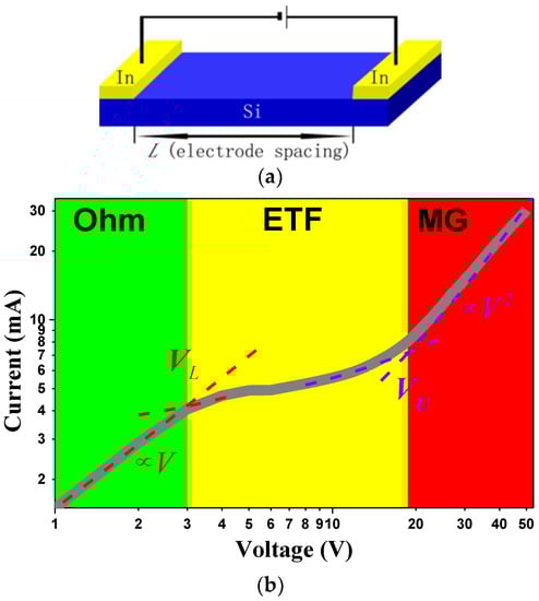
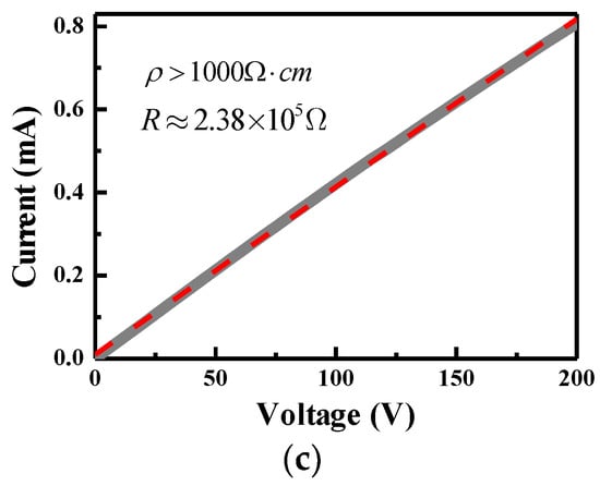
Figure 1.
I–V curves of In/n-Si/In devices. (a) The schematic measurement configuration. Two-terminal devices In/n-Si/In are fabricated by making indium ohmic contacts on n-doped monocrystalline silicon with <111> crystallographic orientation. L is the spacing between two electrodes. (b) I–V curve of In/n-Si/In device 0129-1# at room temperature with resistance 690 Ω and carrier density ~2.1 × 1014 cm−3. L = 2 mm and the applied voltage is in the range from zero to 50 V. VL is defined as the intersection of the tangent extension cords of the I–V curve in the Ohmic and effective trap-filling (ETF) regimes; likewise, VU is the intersection of those in ETF and Mott–Gurney (MG). Thus the Ohm, ETF, and MG regimes are distinguished by two critical voltages. Green, yellow, and red rectangular sections represent Ohm, ETF, and MG regimes respectively. (c) I–V curve of In/n-Si/In device 0114-1# with L = 5 mm measured at room temperature. The resistance is 2.38 × 10⁵ Ω, and the resistivity is larger than 1000 Ω∙cm. The applied voltage is in the range from zero to 200 V. Red dash line is the linear fitting to illustrate the linearity of the Ohmic regime.
The samples were heavily doped n-Si with resistivity 10–20 Ω∙cm and carrier density ~2.1 × 1014 cm−3 at room temperature. We considered that the observed SCE manifested the role of dopants on the motions of injected carriers under an external electric field [1,2,3,4,5,6]. The ionized dopants, which were in fact the effective traps for carriers in a band gap, exert a push-back effect on the motions of carriers. Therefore, under a high electric field, the effect of a space charge limitation on the conduction band is much more significant [1,2]. However, while dopants dominate the dynamics of carrier transport, SCE may hardly be observed at low voltages in light-doped semiconductors due to the absence of effective traps. Figure 1c demonstrates an I–V curve observed in In/n-Si/In device 0114-1#, with the resistivity of n-Si being higher than 1000 Ω∙cm. The linear Ohmic regime holds up to 200 V, reaching the maximum output voltage of Keithley 4200. These observations are different from the report by M. P. Delmo et al. for light-doped silicon [7]. The discrepancy may be attributed to the distribution of dopants along the surface and the energy level of dopants in the band gap. Our previous work showed that a large magnetoresistance and the successive Ohmic and MG regimes could be observed in a current perpendicular to plane (CPP) configuration [6], which can be well simulated by a model proposed by Zhang and Pantelides [2]. In fact, it has been predicted in theory that an ETF regime could be “stretched” to different voltage ranges by the concentration of dopants [1]. More detailed work may be able to probe a single, deep, trap level with various concentrations of dopants from multiple ETF regimes as suggested by Zhang and Pantelides [2].
SCE leads to a non-uniform distribution of internal voltages between electrodes [1,2,3,4,5,6,7,8]. Figure 2a shows I–V curves of device 0129-7# with a different L value. A longer L corresponds to higher resistance; hence, the I–V curve shifts down with an increase in L. With the same definition for the two critical voltages as marked in Figure 1, VL and VU versus L are obtained, as shown in Figure 2b. The voltage difference between VU and VL is ΔV. It is noted that both VU and ΔV are proportional to L2. The L dependence of the critical voltages exhibits a non-uniform electric field distribution along a sample in a nonlinear regime due to the screening effect of free carriers [1,2,3,7]. Next, the concentrations of ionized donors and of deep traps can be estimated from VL and VU according to [1]:
and
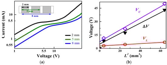
Figure 2.
Electrode spacing dependence of two critical voltages. (a) Black, green, and blue curves are I–V curves with electrode spacing L of 2, 5, and 8 mm measured at room temperature for device 0129-7#. The inserted figure at the left top is the schematic setup, in which the white squares represent indium electrodes. (b) The lower and upper critical voltages, VL and VU, as well as their difference and ΔV = VU − VL, versus the square of electrode spacing L2. Red, purple, and black data illustrate VL, VU, and ΔV respectively. All of them exhibit a linear relationship with L2.
Here, ε is the dielectric constant of silicon (ε = 12 for simplicity), L is the electrode spacing, and e is the electric charge constant. Both ionized donors and deep traps originated from dopants. Although the electric field was non-uniform in the ETF and MG regimes, and were constantly obtained from the above equations, which is in agreement with the theoretical prediction for homogeneous materials [1]. In fact, it was also the physical origin for the spatial distribution of the internal voltage difference in the MG regime as reported by M. P. Delmo et al. [7].
As mentioned above, the ionization and filling of dopants are voltage-dependent. It is noted that the dynamics of ionization and filling may undergo a relaxation under an external electric field due to the accumulation or dissipation of localized charges. Consequently, SCE could have voltage history dependence. Figure 3a demonstrates a voltage-dependent RS effect induced by SCE in a heavily doped n-Si with L = 8 mm (1126-1#). The applied voltage starts from zero up to the positive maximum, reverses down to the negative maximum, and finally comes back to zero. The measured current experiences four distinct processes, labeled as S1, S2, S3, and S4 in sequence (S for step). S1 represents the increasing branch of the I–V curve with the voltage increase, while S2 represents the decreasing one in Figure 3a. It was observed that S2 does not coincide with that of S1 when the voltage is higher than 6 V. Ionization becomes increasingly dominant in S2, so S2 has a lower resistance than S1. As the applied voltage is lower than 6 V, filling and ionization are dynamically balanced. Then, S2 overlaps with S1 exactly, as enlarged in the left top of Figure 3a. S1 and S2 form an RS loop in the first quadrant. While the polarity of the applied voltage is reversed in the third quadrant, the above process repeats. Finally, a complete RS loop comes into being. These observations indicate that RS in monocrystalline silicon is solely related to SCE, so the current Joule heating effect could be ruled out. Therefore, it is termed as SCE–RS.
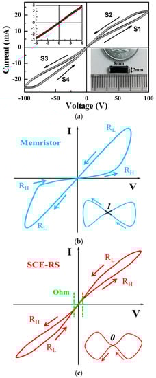
Figure 3.
Space charge effect-resistance switching SCE–RS loops. (a) SCE–RS loop of device 1126-1# with L = 8 mm and sample width of 2 mm. The top left insert illustrates its enlarged plot between ± 6 V. The bottom right insert is the photo of In/n-Si/In device 1126-1#. (b,c) The schematic plots for SCE–RS and memristor respectively. RH and RL represent the high and low resistance states. The black arrows help to differentiate the direction of the applied voltage. Ohmic regime is emphasized in the SCE–RS loop between two green dash lines, while it does not exist in the memristor. The bottom right inserts in (b,c) illustrate the topology of the loops of SCE–RS and memristor respectively.
It is well known that there is another RS effect in solid devices referring to the memristor [9,10,11,12,13,14,15,16,17,18,19,20]. Both the memristor and SCE–RS are nonlinear devices with an RS effect at a high electric field, as shown by schematic plots in Figure 3b,c. However, they differ from each other in the following aspects, including the type of loop, the underlying physics, and materials. First, the memristor loop has a cross around the zero voltage [9,10,11,12,13,14,15,16,17,18,19,20], while the SCE–RS loop has rotational symmetry because of the existence of a linear Ohmic regime. In mathematics, the topological invariants are 1 and 0 for the loops of memristor and SCE–RS respectively, as illustrated in the inserts of Figure 3b,c. The proposed classification might be useful to explore a new type of RS device from the shape of the loop in the view of technology. Secondly, the microscopic nature of a memristor is the voltage-dependent ionic re-arrangement [7,8,9,10,11,12,13,14], which is achieved mainly by the so-called filament effect. Since the hysteresis of ionic migration always exists, the memory effect holds in the whole range of the applied voltage. On the other hand, SCE–RS depends on the dynamics of carriers at a high electric field. Filling and ionization are dynamically balanced in Ohmic regime; thus, the memory effect disappears at zero voltage. Thirdly, the filament effect and its related devices have been realized in polycrystalline oxides, amorphous semiconductors, or nanowires with nanoscale devices [10,11,12,13,14,15,16,17]. However, in the present work, SCE–RS is achieved in the millimeter scale monocrystalline device. In such a case, the filament effect can be ruled out absolutely.
Since SCE–RS is induced by the dynamics of carriers instead of an ion filament effect, with a decrease in thermal disturbance, SCE and SCE–RS are supposed to appear at a lower electric field [18]. Figure 4 shows the temperature dependence of the normalized critical voltages measured in a doped n-Si sample 1016-1# with L = 2 mm. In general, the critical voltages decline with a decrease in temperature. Therefore, the SCE–RS loop shows up at lower voltage. Two SCE–RS loops, measured at 30 and 50 K, are shown in the inserted figure, and the data measured at 300 K in the same voltage range are presented together for comparison. Both the lower and upper critical voltages decrease abruptly from 300 K and slightly between 150 K and 20 K. Assuming the density of states of dopants is exponentially distributed [2,3,4,5,6], the ionization suppression of dopants with shallow levels needs a lower thermal energy, and its density of states is high, resulting in the abrupt decline of the critical voltages initially. The ionization suppression of dopants with deep band sites needs higher energy, but its density of states is relatively small. Hence a slight decline in the critical voltages from 150 K to 20 K is acceptable. In the case of the ion filament effect, a memristor needs an ionic rearrangement, and the ability of ionic migration decreases at low temperatures. Thus, a higher working electric field is needed for a memristor at low temperatures, as reported by Y.J. Dong et al. in Si nanowires [16].
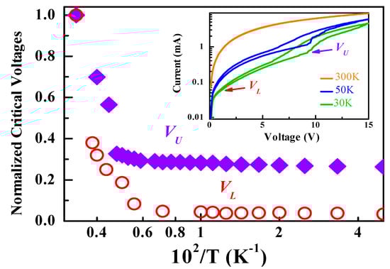
Figure 4.
Temperature dependence of two critical voltages. The temperature dependence of the normalized critical voltages measured in device 1016-1# with L = 2 mm in the range of 20 K to 300 K. Insert, two SCE–RS loops at 30 and 50 K. The data measured at 300 K is presented in the insert for comparison.
Finally, Figure 5a shows the influence of a magnetic field on the I–V curve of device 0129-1# at room temperature. The inserted figure is the schematic measurement configuration. A magnetic field was applied perpendicularly to the sample surface and the direction of the current. The magnetic field suppresses the current all through the I–V curve, and its influence is more significant in the MG regime. The magnetoresistance in the MG regime reaches 20% under 2T field, which is almost 300% enhanced compared with that in Ohmic regime. It was noted that the value of magnetoresistance observed in our heavily doped samples was smaller than that of lightly doped ones in the previous reports [7,21,22,23]. But their common point lies in the enhanced magnetoresistance appearing in nonlinear regimes. The suppression by the magnetic field on the I–V curve in Ohm, ETF and MG regimes is different; hence, both VL and VU may shift. However, as shown in Figure 5b, the variation of VL is negligible compared with the monotonic increase of VU under a magnetic field. Although the influence of a magnetic field on and has not been discussed theoretically [1,2,3,4,5], from an experimental point, by Equations (1) and (2), and can be estimated from the two critical voltages. Figure 5c shows that both and monotonically increase under magnetic field; meanwhile, is always larger than in any given magnetic field. We propose that the enhancement of is caused by the Zeeman effect on the shallow dopants with half-filled p states (3s23p3) due to the level splitting under a magnetic field. On the other hand, a magnetic field prolongs the relaxation time of carriers combining into neighboring localized states, resulting in the enhancement of under a magnetic field. In accordance, the SCE–RS loop can be modulated by a magnetic field. In Figure 6, red, green, and blue data are SCE–RS loops measured in an 8 mm n-doped Si sample 1126-1# under 0, 5, and 10 kG magnetic field at room temperature. With the increase in magnetic field, the SCE–RS loop is suppressed and the resistance enhances. The magnetic field suppression is negligible in the Ohmic regime, which is consistent with the observation in Figure 5. Evidently, magnetic-dependent SCE–RS loops are the hybrid effect of the modulation by both an electric and magnetic field on SCE. This is clearly different from magnetic field modulation on the RS effect reported in magnetic/semiconductor hybrid devices [20,24]. In comparison to the memristors, SEC–RS originates from the nonlinear carrier transport and is therefore more susceptible to magnetic fields.
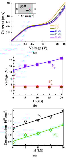
Figure 5.
Magnetic field dependence of two critical voltages. (a) I–V curves of device 0129-1# with L = 2 mm under different magnetic fields measured at room temperature. Red and purple dash lines represent laws of Ohmic and MG, respectively. Insert, magnetic field applied perpendicularly to the sample surface and the current. (b) Magnetic field dependence of VL and VU. (c) Magnetic field dependence of and . In (b,c), solid lines are the linear fitting guided by eyes to illustrate the magnetic field dependence of those parameters experimentally.
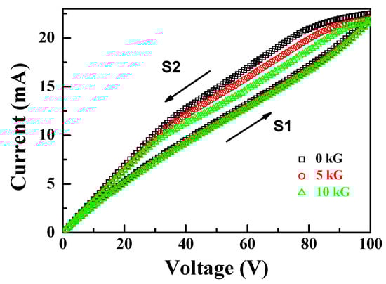
Figure 6.
Magnetic SCE–RS loops. Red, green, and blue data are SCE–RS loops measured in an 8 mm, n-doped, Si device (1126-1#) under the magnetic fields of 0, 5, and 10 kG at room temperature. Black arrows illustrate the sequence of voltage applied.
In recent years, a significant volume of research has focused on non-volatile memory components in polycrystalline or amorphous materials which underlie the voltage-dependent ionic re-arrangement in nanometer-scale oxide devices. In a single crystal, ionic migration is absent. SCE and the resultant SCE–RS merely originate from the fast dynamics of carriers in a space charge regime modulated by dopants under an external electric field. There is no doubt that a non-volatile memory cell in polycrystalline or amorphous materials is crucial for recording/extracting information. However, the high-field nonlinearity, as well as the volatile RS loops, may provide a way to understand the fast dynamics of carriers in crystals. The present work reports some preliminary experimental observations. It is also expected that the irreversible carrier’s dynamics and its related experimental characteristics could receive more attention. In addition, if a memristor is assumed as an analogy for memorization in artificial intelligence, an SCE–RS device could represent a stimuli-response-forgetting process. Both the persistence (remembering) and transience (forgetting) of memory are important to a neural analog circuit. [25] Will people expect to switch these two types of processes in the same cell via feedback signals in the near future? In this sense, SCE–RS may have a potential to extend the functionality of RS devices in neural circuits, especially for all silicon-based devices.
Author Contributions
X.J. fabricated and measured the samples and analyzed the data. H.W. supervised the project. H.W. and X.J. wrote the manuscript. C.F. helped to check the details of manuscript independently.
Funding
This work was financially supported by the National Natural Science Foundation of China (NSFC) with Grant No. 11274233, National Key Scientific Instrument and Equipment Development Project of China with Grant No. 2012YQ140005 and Beijing education committee under grant No. KM201810028006.
Conflicts of Interest
The authors declare no conflict of interest.
References
- Zhang, X.-G.; Pantelides, S.T. Theory of Space Charge Limited Currents. Phys. Rev. Lett. 2012, 108, 266602–266606. [Google Scholar] [CrossRef] [PubMed]
- Rose, A. Space-charge-limited currents in solids. Phys. Rev. 1955, 97, 1538–1544. [Google Scholar] [CrossRef]
- Lampert, M.A. Simplified theory of space-charge-limited currents in an insulator with traps. Phys. Rev. 1956, 103, 1648–1656. [Google Scholar] [CrossRef]
- Zhang, Y.; Blom, P.W.M. Field-assisted ionization of molecular doping in conjugated polymers. Org. Electron. 2010, 11, 1261–1267. [Google Scholar] [CrossRef]
- Zhang, Y.; de Boer, B.; Blom, P.W.M. Trap-free electron transport in poly(p-phenylene vinylene) by deactivation of traps with n-type doping. Phys. Rev. B 2010, 81, 085201–085205. [Google Scholar] [CrossRef]
- Liu, Y.; Wang, H.; Jin, X.; Zhang, M. The space charge limited current and huge linear magnetoresistance in silicon. Sci. Rep. 2018, 8, 775. [Google Scholar] [CrossRef] [PubMed]
- Delmo, M.P.; Yamamoto, S.; Kasai1, S.; Ono, T.; Kobayashi, K. Large positive magnetoresistive effect in silicon induced by the space-charge effect. Nature 2009, 457, 1112–1115. [Google Scholar] [CrossRef]
- Mott, N.F.; Gurney, R.W. Electronic Processes in Ionic Crystals; Oxford University Press: London, UK, 1940. [Google Scholar]
- Prodromakis, T.; Toumazou, C.; Chua, L. Two centuries of memristors. Nat. Mater. 2012, 11, 478–481. [Google Scholar] [CrossRef]
- Strukov, D.B.; Snider, G.S.; Stewar, D.R.; Williams, R.S. The missing memristor found. Nature 2008, 459, 7250. [Google Scholar] [CrossRef]
- Lee, M.-J.; Lee, C.B.; Lee, D.; Chang, M.; Hur, J.H.; Kim, Y.-B.; Kim, C.-J.; Seo, D.H.; Seo, S.; Chung, U.-I.; et al. A fast, high-endurance and scalable non-volatile memory device made from asymmetric Ta2O5−x/TaO2−x bilayer structures. Nat. Mater. 2011, 10, 625–630. [Google Scholar] [CrossRef]
- Kwon, D.-H.; Kim, K.M.; Jang, J.H.; Jeon, J.M.; Lee, M.H.; Kim, G.H.; Li, X.-S.; Park, G.-S.; Lee, B.; Han, S.; et al. Atomic structure of conducting nanofilaments in TiO2 resistive switching memory. Nat. Nanotechnol. 2010, 5, 148–153. [Google Scholar] [CrossRef] [PubMed]
- Jafar, M.; Haneman, D. Possible quantum effects in amorphous silicon double Schottky diodes. Phys. Rev. B 1993, 47, 10911–10914. [Google Scholar] [CrossRef]
- Jafar, M.; Haneman, D. Switching in amorphous-silicon devices. Phys. Rev. B 1994, 49, 13611–13615. [Google Scholar] [CrossRef]
- Hu, J.; Branz, H.M.; Crandall, R.S.; Ward, S.; Wang, Q. Switching and filament formation in hot-wire CVD p-type a-Si:H devices. Thin Solid Films 2003, 430, 249–252. [Google Scholar] [CrossRef]
- Dong, Y.; Yu, G.; McAlpine, M.C.; Lu, W.; Lieber, C.M. Si a-Si CoreShell Nanowires as Nonvolatile Crossbar Switches. Nano Lett. 2008, 8, 386–391. [Google Scholar] [CrossRef] [PubMed]
- Seo, J.W.; Baik, S.J.; Kang, S.J.; Hong, Y.H.; Yang, J.; Fang, L.; Lim, K.S. Evidence of Al induced conducting filament formation in Al/amorphous silicon/Al resistive switching memory device. Appl. Phys. Lett. 2010, 96, 053504. [Google Scholar]
- Chua, L.O. Memristor—The missing circuit element. IEEE Trans. Circuit Theory 1971, 18, 507–519. [Google Scholar] [CrossRef]
- Chua, L. Resistance switching memories are memristors. Appl. Phys. A 2011, 102, 765–783. [Google Scholar] [CrossRef]
- Chen, G.; Song, C.; Chen, C.; Gao, S.; Zeng, F.; Pan, F. Resistive Switching and Magnetic Modulation in Cobalt-Doped ZnO. Adv. Mater. 2012, 24, 3515–3520. [Google Scholar] [CrossRef]
- Delmo, M.P.; Kasai, S.; Kobayashi, K.; Ono, T. Current-controlled magnetoresistance in silicon in non-Ohmic transport regimes. Appl. Phys. Lett. 2009, 95, 132106–132108. [Google Scholar] [CrossRef]
- Wu, L.H.; Zhang, X.; Vanacken, J.; Schildermans, N.; Wan, C.H.; Moshchalkov, V.V. Room-temperature non-saturating magnetoresistance of intrinsic bulk silicon in high pulsed magnetic fields. Appl. Phys. Lett. 2011, 98, 112113. [Google Scholar] [CrossRef]
- Porter, N.A.; Marrows, C.H. Dependence of magnetoresistance on dopant density in phosphorous doped silicon. J. Appl. Phys. 2011, 109, 07C703. [Google Scholar] [CrossRef]
- Thakare, V.; Xing, G.Z.; Peng, H.Y.; Rana, A.; Game, O.; Kumar, P.A.; Banpurkar, A.; Kolekar, Y.; Ghosh, K.; Wu, T.; et al. High sensitivity low field magnetically gated resistive switching in CoFe2O4/La0.66Sr0.34MnO3 heterostructure. Appl. Phys. Lett. 2012, 100, 172412. [Google Scholar] [CrossRef]
- Richards, B.A.; Frankland, P.W. The Persistence and Transience of Memory. Neuron 2017, 94, 1071–1084. [Google Scholar] [CrossRef] [PubMed]
© 2019 by the authors. Licensee MDPI, Basel, Switzerland. This article is an open access article distributed under the terms and conditions of the Creative Commons Attribution (CC BY) license (http://creativecommons.org/licenses/by/4.0/).