Abstract
A polarization-insensitive phase modulator concept is presented, based on an embedded silicon-graphene-silicon waveguide. Simulation results show that the effective mode index of both transverse electric (TE) and transverse magnetic (TM) modes in the silicon-graphene-silicon waveguide undergoes almost the same variations under different biases across a broad wavelength range, in which the real-part difference is less than 1.2 × 10⁻³. Based on that, a polarization-insensitive phase modulator is demonstrated, with a 3-dB modulation bandwidth of 135.6 GHz and a wavelength range of over 500 nm. Moreover, it has a compact size of 60 μm, and a low insertion loss of 2.12 dB. The proposed polarization-insensitive waveguide structure could be also applied to Mach-Zehnder modulators and electro-absorption modulators.
1. Introduction
Electro-optic phase modulators (PMs) have been widely and intensively investigated for their applications in advanced optical communication systems, thanks to their intrinsically bias-free and linear modulation properties [1,2,3]. Most PMs are based on substrates of low crystal symmetry and require special polarization control for the incoming optical signal, due to their polarization sensitivity. However, the present trend of optical communication networking dictates the need for polarization-independent optical devices, especially at nodal junctions [4].
Several methods have been proposed for realizing polarization-insensitive modulators by using, for example, electrode sets [4,5,6], bidirectional modulation [7,8,9,10], or tensile strained quantum wells [11,12,13]. The most effective method is to introduce two independent electrode sets for the desired transverse electric (TE) and transverse magnetic (TM) polarizations. However, this method leads to have long waveguides and large operating voltages, limited by the small change in the refractive index change of common electrooptic crystals [5], which is not efficient for high-speed modulation [7]. The bidirectional modulation method is based on bidirectional phase modulation for the TE and TM modes through a Sagnac loop, which overcomes the intrinsic polarization dependence of silicon photonic modulators [8]. In the case of bidirectional operation, the device’s bandwidth is limited to several GHz, due to the counter-propagation of the electrical and optical waves [9]. Strained quantum wells have been successfully demonstrated for realizing polarization insensitivity operations with very compact structures. The major limitation lies in large insertion loss and high temperature sensitivity [13]. Therefore, polarization-insensitive PMs with large bandwidth, low insertion loss, and compact size, are of great interest.
Recently, graphene has attracted much interest in optoelectronic devices, due to its excellent electronic and optical properties [14]. Moreover, its electrical conductivity can be tuned by electrostatic gating, as well as dielectric-metal transition, in a near-infrared regime [15]. Graphene embedded silicon modulators have been proven to be superior against traditional modulators [16,17,18,19,20]. In this paper, we propose, for the first time to the best of our knowledge, a polarization-insensitive PM based on an embedded silicon-graphene-silicon waveguide. We design a novel sandwiched waveguide structure, in which an inner waveguide is embedded into an outer one. The polarization dependence of the proposed waveguide has been studied for achieving the polarization-insensitive modulation with the finite element method. Based on the proposed polarization-insensitive waveguide, the polarization-insensitive PM is demonstrated with a wavelength range of over 500 nm, and a modulation bandwidth of 135.6 GHz through numerical simulations. The proposed PM also has a compact size and low insertion loss.
2. Polarization-Insensitive Waveguide Structure
As is known, graphene is an attractive material for electro-optic modulators due to its strong interaction with light and electrically-controllable optical conductivity [14]. It has been reported that the structure of a sandwiched graphene-silicon waveguide will enhance the interaction between graphene and light [21]. However, sandwiched graphene-silicon waveguides are generally polarization-sensitive, since the TE and TM modes experience an unbalanced refractive index and loss on the horizontal and vertical axes. To achieve polarization insensitivity, the structure and size of the graphene waveguide should be specifically designed, since they have much influence on the effective refractive index (neff) for TE and TM modes. Here, we design a novel embedded structure in which an inner waveguide is embedded into an outer one. As is shown in Figure 1, an inner silicon waveguide with 400 nm width and 460 nm height is surrounded by two 0.7 nm graphene layers. The two graphene layers, which are separated by a 10 nm thick Si3N4 spacer, are also surrounded by an outer waveguide with the width and height of 800 nm and 800 nm. For fabrication, it is better to replacing the rectangular silicon-graphene waveguide with a slanted silicon-graphene waveguide for the inner waveguide [22]. Metal electrodes are in contact with the graphene layers, so that the two graphene layers can form capacitor structures.
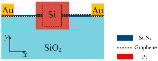
Figure 1.
The cross-sectional view of the polarization-insensitive waveguide.
For a polarization-insensitive waveguide, the real-part difference of an effective refractive index between TE and TM modes (ΔRe = Re(neff_TE) − Re(neff_TM)) should be less than 5 × 10⁻⁴ [23], and the insertion loss difference between TE and TM modes (Δα = α(TE) − α(TM)), which results from the imaginary-part difference of the refractive effective refractive index between TE and TM modes, should be less than 4 × 10⁻³ dB/μm [11,24,25,26], such as the polarization sensitive < 1 dB with the waveguide length of 250 μm (i.e., 4 × 10⁻³ dB/μm) [26]. The insertion loss can be calculated with α = −40πlge·Im(neff)/λ. The outer waveguide around the small one enhances light-graphene interaction which is the key design element for achieving effective electro-optic modulation. In the horizontal and vertical directions, the light in the waveguide is influenced by the graphene, to make sure that the waveguide is polarization-insensitive to the TM and TE modes. With the finite element method, ΔRe and Δα of the proposed waveguide are calculated in the case of different widths and heights of the inner waveguide, as shown in Figure 2. In the simulation, there is no voltage on the graphene and the incident light is set as λ = 1550 nm. From Figure 2a, it can be observed that ΔRe and Δα are kept to be less than 1.5 × 10⁻³ and 1.4 × 10⁻² dB/μm, respectively, with the inner waveguide width ranging from 300 nm to 500 nm. From Figure 2b, it can be observed that ΔRe and Δα are kept to be less than 1.5 × 10⁻³ and 4 × 10⁻² dB/μm, respectively, with the inner waveguide height ranging from 410 nm to 530 nm. The waveguide width and height can be optimized to make sure there is a small value of ΔRe and Δα for a polarization-insensitive waveguide.
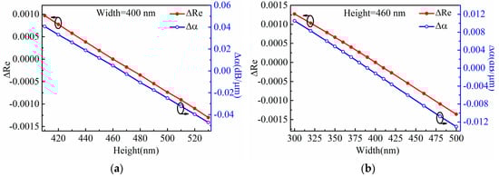
Figure 2.
Difference of the real- and imaginary-part of effective refractive index between TE and TM modes in the case of different waveguide widths (a) and heights (b).
3. Graphene-Based Polarization-Insensitive Phase Modulator
The graphene’s complex optical conductance σ = σintra + σinter can be deduced from Kubo formalisms [27]:
where σintra and σinter are the intraband conductivity and interband conductivity of the graphene, σ0 is the universal optical conductance, ћ is reduced Planck constant, and ω = 2πc/λ is the angular frequency of incident light. Γ1 = 1/τ1 and Γ2 = 1/τ2, where τ1 and τ2 are intraband relaxation time and interband relaxation time of the graphene, respectively. The chemical potential μc of the graphene is related to the applied voltage Vg by μc = ћv = F (π|η(Vg + V0)|)1/2 [28], with the Fermi velocity vF ≈ 9.5 × 10⁵ m/s and the voltage offset V0 caused by the natural doping. H = (ε0ε)/(ed) is a constant, ε and d represent the permittivity and distance of the dielectric between the two graphene layers, and e is the charge of an electron.
The permittivity of graphene εg is related to the optical conductance σ by εg = 1 + i·σ/(ωε0Δ). Figure 3 shows the permittivity of graphene as a function of the chemical potential μc, in which Δ = 0.7 nm stands for the single layer graphene’s effective thickness. As shown in Figure 3, graphene’s permittivity gets close to zero when the chemical potential (μc) is around 0.5 eV, and the point is called the epsilon near zero (ENZ) point. In our simulation, the typical parameters are λ = 1550 nm, T = 300 K, τ1 = 1.5 × 10⁻¹⁴ s and τ2 = 1.2 × 10⁻¹² s [29].
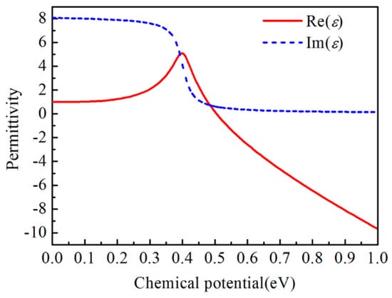
Figure 3.
Permittivity of graphene under different chemical potentials.
As is known, the electrically-controllable optical conductivity of graphene can effectively affect a waveguide mode’s effective refractive index. We have designed a polarization-insensitive phase modulator, based on the proposed waveguide shown in Figure 1. The inner silicon waveguide with the width and height of 400 nm and 460 nm, respectively, is surrounded by two 0.7 nm graphene layers. The two graphene layers, which are separated by a 10 nm thick Si3N4 spacer, are also surrounded by the outer waveguide, with a width and height of 800 nm and 800 nm, respectively. Figure 4a,b show the electric fields of the TE and TM mode in the case of μc = 0.5 eV. Figure 4c,d show the effective refractive index of the TE and TM mode in the case of different chemical potentials of graphene. Graphene’s chemical potential can be changed by applying different voltages on the electrodes of the proposed waveguide. The insets in Figure 4c,d show ΔRe and Δα in the case of different chemical potentials of graphene, respectively, the maximum ΔRe of 1.2 × 10⁻⁴, and Δα of 2.9 × 10⁻³ dB/μm verifies the polarization-insensitive modulation of the proposed waveguide structure.
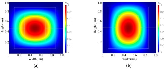
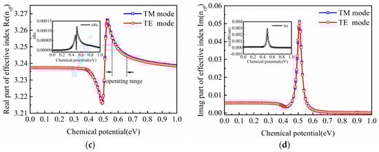
Figure 4.
(a,b) are the electric fields of the TE and TM modes, respectively; (c,d) are the real- and imaginary-part of effective refractive index of TE and TM modes in the cases of different chemical potentials of graphene, respectively.
As is shown in Figure 4c, the real-part of the effective refractive index Re(neff) for the waveguide changes sharply when 0.4 eV < μc < 0.7 eV. The phase change can be simply achieved in this range of μc. Figure 4d shows that the image-part of the effective refractive index, Im(neff), experiences a large change in the range of 0.45 eV < μc < 0.55 eV, and the Im(neff) is also large for the loss in this range. To compromise a relative large phase shift and low absorption α within the range of μc, we set the operating range of 0.56 eV < μc < 0.66 eV, corresponding to the operating voltage of 4.36 V < Vg < 6.1 V. The maximum variation of the real-part of the effective refractive index, Δneff = 0.013, which seems to be much larger than conventional electro-optic modulator, is realized by LiNbO3 (maximum value Δneff = 0.0016) [30]. The phase shift is related to Δneff by Δφ = (2π/λ) × Δneff × L and the length of π phase shift Lπ = 59.6 μm. The approximate linear relationship between phase and chemical potential in the range of 0.56 eV < μc < 0.66 eV for a 60 μm long waveguides is shown in Figure 5a with a red line. To evaluate the loss in the selected range, propagation length Lp is studied and related to Im(neff) by Lp = 1/(2Im(neff)2π/λ) [31], which is the length when output power decays to 1/e of its input power, as shown in Figure 5a with a blue line. When μc = 0.56 eV, the loss index is 0.063 dB/μm and the propagation length Lp = 69.1 μm, while for μc = 0.66 eV, the propagation length is 343 μm. The insertion loss is less than 2.12 dB at μc = 0.6 eV for a 60 μm long waveguide. In Figure 5b, the proposed PM operates with polarization insensitivity when the incident light wavelength is from 1300 nm to 1800 nm.
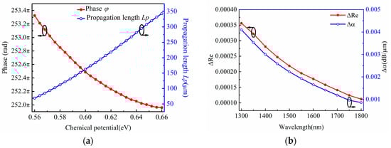
Figure 5.
(a) Phase change and propagation length Lp in the range of 0.56 eV < μc < 0.66 eV, with the incident optical wavelength of 1550 nm; (b) Difference of the real- and imaginary-part of the effective refractive index between TE and TM modes in the case of different wavelengths.
The equivalent electrical circuit model of the proposed polarization-insensitive PM is shown in Figure 6a. The Rtotal is the equivalent resistance of each side of graphene and composed of the metal-graphene contact resistance Rc and the resistance of graphene Rg [32], and the Rtotal is almost offered by the metal-graphene contact resistance, so here we set Rtotal ≈ Rc = 400 Ω-μm [33]. In Figure 6b, the total capacitance consists of three parts, C = C1 + C2 + C3. Each part can be calculated by Ci = ε0εrSi/di (i = 1,2,3) and εr is the relative permittivity between the two graphene layers. Si is stands for the area of the plate capacitor, and di is the distance of the plate capacitor. With the function of f3dB = 1/(2π·2RtotalC), the 3-dB modulation bandwidth of the proposed PM is estimated to be f3dB = 135.6 GHz.
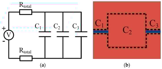
Figure 6.
(a) Equivalent electrical circuit model of the proposed phase modulator (PM); (b) Components of the total capacitance.
In a practical fabrication process [34,35], some important processes of the designed polarization-insensitive phase modulator based on embedded silicon-graphene-silicon waveguide are as follows: firstly, the ways of acquitting, transferring, and processing monolayer graphene are very important. Through chemical vapor deposition, a chip-sized graphene layer can be obtained on Cu film and is then protected by 200-nm thick poly (methyl methacrylate) film. The graphene sheet is rinsed and transferred on the fabricated Si waveguide using the FeCl3 solution. E-beam lithography is then used to define the active region, and oxygen plasma is applied to remove the undesired graphene on one side of the waveguide, leaving the other side for metallization. Secondly, the Si waveguide fabrication with a groove can be realized by E-beam lithography, combined with the inductively coupled plasma etching process. Thermal evaporation is used to deposit metal for electrodes.
4. Conclusions
To summarize, we propose a novel polarization-insensitive PM, based on an embedded silicon-graphene-silicon waveguide, and demonstrate a graphene-based polarization-insensitive phase modulator with the embedded waveguide. The phase modulator shows a 3-dB modulation bandwidth of 135.6 GHz and an optical bandwidth of over 500 nm. Moreover, it has a compact size of 60 µm long and low insertion loss of 2.12 dB.
Author Contributions
X.Z. and S.Z. conceived the paper, and discussed the novel polarization-insensitive PM based on an embedded silicon-graphene-silicon waveguide. X.Z. and Y.Z. (Yujia Zhang) designed the graphene-based phase modulator model, and performed the simulation. Y.Y. and Z.L. analyzed the data and conducted the figure drawing. Z.Z., Y.Z. (Yali Zhang) and Y.L. provided some valuable suggestions and revised the paper.
Funding
This research was funded by National Nature Science Foundation of China (No. 61875240, 61421002, 61435010) and Science Foundation for Youths of Sichuan Province (No. 2016JQ0014).
Conflicts of Interest
The authors declare no conflict of interest.
References
- Seeds, A.J.; Williams, K.J. Microwave photonics. J. Lightwave Technol. 2007, 24, 4628–4641. [Google Scholar] [CrossRef]
- Capmany, J.; Mora, J.; Gasulla, I.; Sancho, J.; Lloret, J.; Sales, S. Microwave photonic signal processing. J. Lightwave Technol. 2013, 31, 571–586. [Google Scholar] [CrossRef]
- Lloret, J.; Kumar, R.; Sales, S.; Ramos, F.; Morthier, G.; Mechet, P.; Spuesens, T.; Van Thourhout, D.; Olivier, N.; Fédéli, J.M.; et al. Ultracompact electro-optic phase modulator based on III–V-on-silicon microdisk resonator. Opt. Lett. 2012, 37, 2379–2381. [Google Scholar] [CrossRef] [PubMed]
- Oh, H.H.; Ahn, S.W.; Shin, S.Y. Polarisation-independent phase modulator using electro-optic polymer. Electron. Lett. 2000, 36, 969–970. [Google Scholar] [CrossRef]
- Kaplan, A.; Ruschin, S. Layout for polarization insensitive modulation in LiNbO3 waveguides. IEEE J. Sel. Top. Quant. 2000, 6, 83–87. [Google Scholar] [CrossRef]
- Donval, A.; Toussaere, E.; Hierle, R.; Zyss, J. Polymer based polarization insensitive amplitude modulator: Conception, technology and demonstration. Synth. Met. 2000, 115, 21–27. [Google Scholar] [CrossRef]
- Li, G.L.; Yu, P.K.L. Optical intensity modulators for digital and analog applications. J. Lightwave Technol. 2003, 21, 2010–2030. [Google Scholar] [CrossRef]
- Schindler, P.C.; Lauermann, M.; Wolf, S.; Korn, D.; Palmer, P.; Koeber, S.; Heni, W.; Ludwig, A.; Schmogrow, R.; Elder, D.L.; et al. Ultra-short silicon-organic hybrid (SOH) modulator for bidirectional polarization-independent operation. In Proceedings of the 2014 European Conference on Optical Communication (ECOC), Cannes, France, 21–25 September 2014; pp. 1–3. [Google Scholar]
- Ng, T.T.; Gosal, D.; Lamas-Linares, A.; Kurtsiefer, C. Sagnac-loop phase shifter with polarization-independent operation. Rev. Sci. Instrum. 2011, 82, 1165. [Google Scholar] [CrossRef]
- Qi, B.; Huang, L.L.; Lo, H.K.; Qian, L. Quantum key distribution based on a Sagnac loop interferometer and polarization-insensitive phase modulators. In Proceedings of the 2006 IEEE International Symposium on Information Theory, Seattle, WA, USA, 9–14 July 2006; pp. 1–4. [Google Scholar]
- Chang, G.E.; Chang, C.O. Tensile-strained Ge/SiGeSn quantum wells for polarization-insensitive electro-absorption waveguide modulators. IEEE J. Quantum Electron. 2012, 48, 533–541. [Google Scholar] [CrossRef]
- Choy, W.C.; Li, E.H. Polarization-insensitive electroabsorption by use of quantum well interdiffusion. Appl. Opt. 1998, 37, 1674–1681. [Google Scholar] [CrossRef]
- Spickermann, R.; Peters, M.G.; Dagli, N. A polarization independent GaAs-AlGaAs electrooptic modulator. IEEE J. Quantum Electron. 1996, 32, 764–769. [Google Scholar] [CrossRef]
- Kim, K.; Choi, J.Y.; Kim, T.; Cho, S.H.; Chung, H.J. A role for graphene in silicon-based semiconductor devices. Nature 2011, 479, 338–344. [Google Scholar] [CrossRef]
- Sensale-Rodriguez, B. Graphene-based optoelectronics. J. Lightwave Technol. 2015, 33, 1100–1108. [Google Scholar] [CrossRef]
- Xu, C.; Jin, Y.C.; Yang, L.C.; Yang, J.Y.; Jiang, X.Q. Characteristics of electro-refractive modulating based on Graphene-Oxide-Silicon waveguide. Opt. Express 2012, 20, 22398–22405. [Google Scholar] [CrossRef]
- Sorianello, V.; Midrio, M.; Romagnoli, M. Design optimization of single and double layer graphene phase modulators in SOI. Opt. Express 2015, 23, 6478–6490. [Google Scholar] [CrossRef]
- Li, W.; Chen, B.G.; Meng, C.; Fang, W.; Xiao, Y.; Li, X.Y.; Hu, Z.F.; Xu, Y.X.; Tong, L.M.; Wang, H.Q.; et al. Ultrafast all-optical graphene modulator. Nano Lett. 2014, 14, 955–959. [Google Scholar] [CrossRef]
- Youngblood, N.; Anugrah, Y.; Ma, R.; Koester, S.J.; Li, M. Multifunctional graphene optical modulator and photodetector integrated on silicon waveguides. Nano Lett. 2014, 14, 2741–2746. [Google Scholar] [CrossRef]
- Das, S.; Salandrino, A.; Wu, J.Z.; Hui, R.Q. Near-infrared electro-optic modulator based on plasmonic grapheme. Opt. Lett. 2015, 40, 1516–1519. [Google Scholar] [CrossRef]
- Lu, Z.L.; Zhao, W.S. Nanoscale electro-optic modulators based on graphene-slot waveguides. JOSA B 2012, 29, 1490–1496. [Google Scholar] [CrossRef]
- Ye, S.W.; Liang, D.; Lu, R.G.; Shah, M.K.; Zou, X.H.; Yang, F.; Yuan, F.; Liu, Y. Polarization independent modulator by partly tilted graphene induced electro-absorption effect. IEEE Photonics Technol. Lett. 2016, 29, 23–26. [Google Scholar] [CrossRef]
- Tang, P.S.; Towner, D.J.; Meier, A.L.; Wessels, B.W. Low-voltage, polarization-insensitive, electro-optic modulator based on a polydomain barium titanate thin film. Appl. Phys. Lett. 2004, 85, 4615–4617. [Google Scholar] [CrossRef]
- Duchet, C.; Boucherez, E.; Fortin, C.; Legouezigou, O. Polarisation-insensitive modulator and influence of propagation direction on bulk electroabsorption. Electron. Lett. 1997, 33, 233–235. [Google Scholar] [CrossRef]
- Qiu, X.M.; Ruan, X.K.; Li, Y.P.; Zhang, F. Multi-layer MOS capacitor based polarization insensitive electro-optic intensity modulator. Opt. Express 2018, 26, 13902–13914. [Google Scholar] [CrossRef]
- Koren, U.; Miller, B.I.; Young, M.G.; Chien, M.; Raybon, G.; Brenner, T.; Ben-Michael, R.; Dreyer, K.; Capik, R.J. Polarisation insensitive semiconductor optical amplifier with integrated electroabsorption modulators. Electron. Lett. 1996, 32, 111–112. [Google Scholar] [CrossRef]
- Gusynin, V.P.; Sharapov, S.G.; Carbotte, J.P. Magneto-optical conductivity in graphene. J. Phys. Condens. 2007, 19, 026222. [Google Scholar] [CrossRef]
- Yang, L.Z.; Hu, T.; Hao, R.; Qiu, C.; Xu, C.; Yu, H.; Xu, Y.; Jiang, X.Q.; Li, Y.B.; Yang, J.Y. Low-chirp high-extinction-ratio modulator based on graphene-silicon waveguide. Opt. Lett. 2013, 14, 2512–2515. [Google Scholar] [CrossRef]
- Gosciniak, J.; Tan, D.T.H. Theoretical investigation of graphene-based photonic modulators. Sci. Rep. 2013, 3, 1897. [Google Scholar] [CrossRef]
- Haruna, M.; Koyama, J. Thermo-optic effect in LiNbO3 for light deflection and switching. Electron. Lett. 1981, 17, 842–844. [Google Scholar] [CrossRef]
- Zhou, F.; Hao, R.; Jin, X.F.; Zhang, X.M.; Li, E.P. A graphene-enhanced fiber-optic phase modulator with large linear dynamic range. IEEE Photonics Technol. Lett. 2014, 26, 1867–1870. [Google Scholar] [CrossRef]
- Nirmalraj, P.N.; Lutz, T.; Kumar, S.; Duesberg, G.S.; Boland, J.J. Nanoscale mapping of electrical resistivity and connectivity in graphene strips and networks. Nano Lett. 2010, 11, 16–22. [Google Scholar] [CrossRef]
- Xia, F.; Perebeinos, V.; Lin, Y.M.; Wu, Y.; Avouris, P. The origins and limits of metal-graphene junction resistance. Nat. Nanotechnol. 2011, 6, 179–184. [Google Scholar] [CrossRef]
- Liu, M.; Yin, X.B.; Ulin-Avila, E.; Geng, B.; Zentgraf, T.; Ju, L.; Wang, F.; Zhang, X. A graghene-based broadband optical modulator. Nature 2011, 474, 64–67. [Google Scholar] [CrossRef]
- Liu, M.; Yin, X.B.; Zhang, X. Double-layer graghene optical modulator. Nano Lett. 2012, 12, 1482–1485. [Google Scholar] [CrossRef]
© 2019 by the authors. Licensee MDPI, Basel, Switzerland. This article is an open access article distributed under the terms and conditions of the Creative Commons Attribution (CC BY) license (http://creativecommons.org/licenses/by/4.0/).