Comparison of Various Factors Affected TID Tolerance in FinFET and Nanowire FET


Abstract
1. Introduction
2. Simulation Methodology
2.1. Design Structure for TID Simulation
2.2. TID Simulation of Various Factors
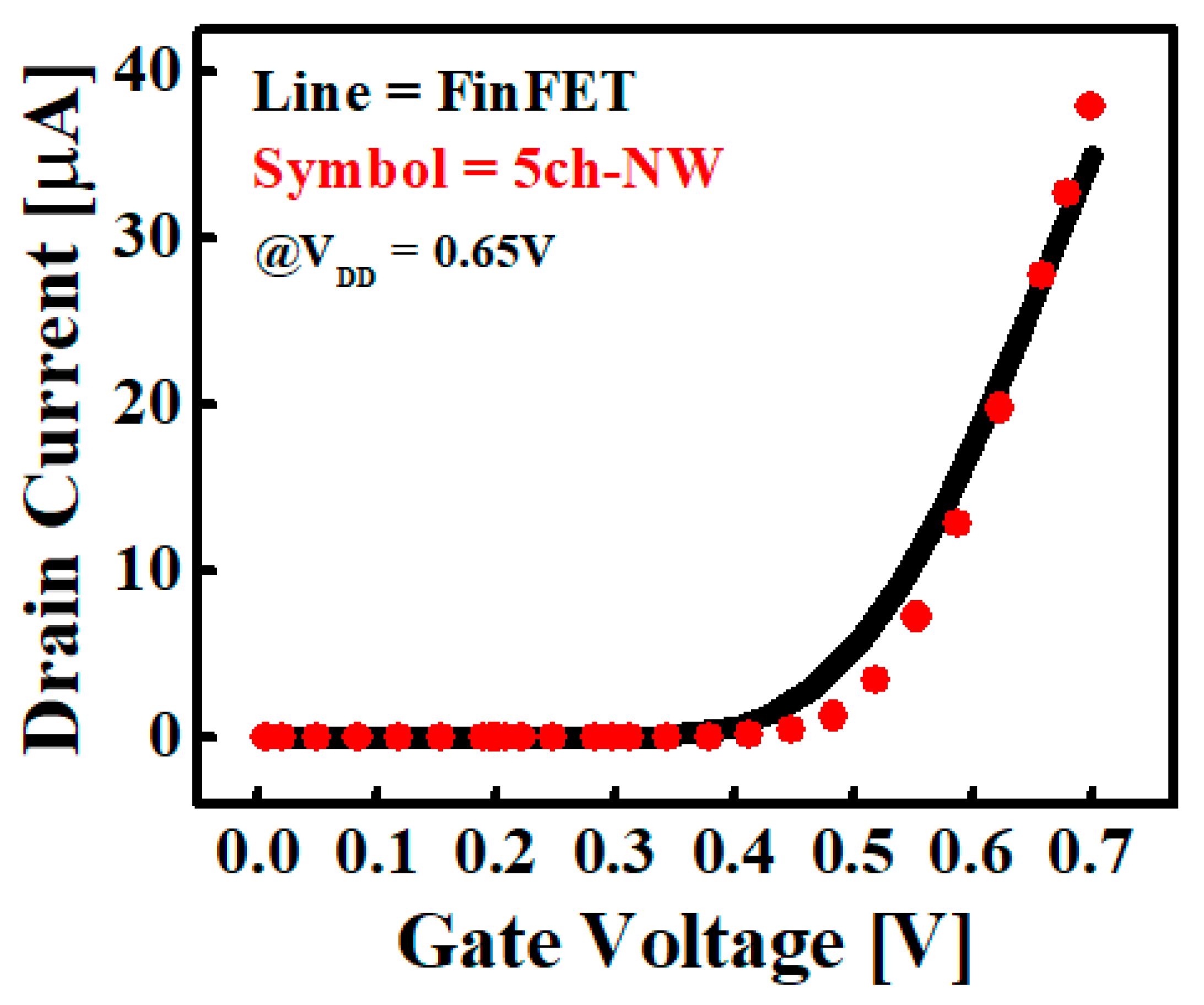
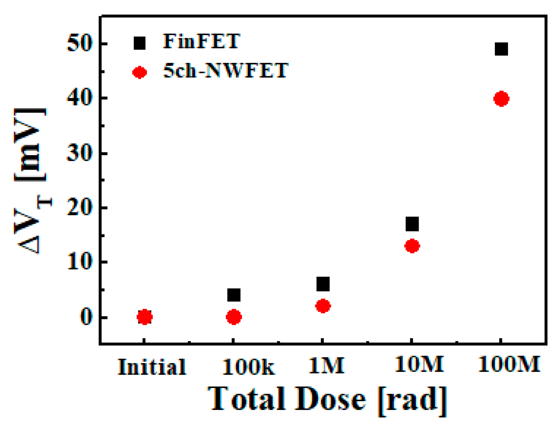
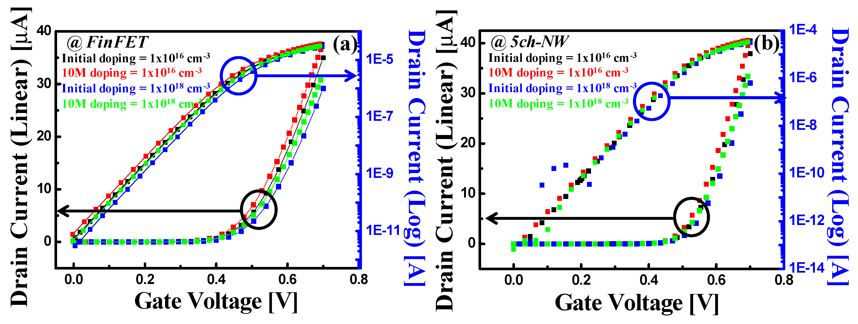
3. Results and Discussion
4. Conclusions
Author Contributions
Funding
Conflicts of Interest
References
- Leroux, P.; Van Koeckhoven, W.; Verbeeck, J.; Van Uffelen, M.; Esqué, S.; Ranz, R.; Damiani, C.; Hamilton, D. Design of a MGy radiation tolerant resolver-to-digital convertor IC for remotely operated maintenance in harsh environments. Fusion Eng. Des. 2014, 89, 2314–2319. [Google Scholar] [CrossRef]
- Haddad, N.F.; Kelly, A.T.; Lawrence, R.K.; Li, B.; Rodgers, J.C.; Ross, J.F.; Warren, K.M.; Weller, R.A.; Mendenhall, M.H.; Reed, R.A. Incremental enhancement of SEU hardened 90 nm CMOS memory cell. IEEE Trans. Nucl. Sci. 2011, 58, 975–980. [Google Scholar] [CrossRef]
- Clark, L.T.; Mohr, K.C.; Holbert, K.E.; Yao, X.; Knudsen, J.; Shah, H. Optimizing radiation hard by design SRAM cells. IEEE Trans. Nucl. Sci. 2007, 54, 2028–2036. [Google Scholar] [CrossRef]
- Gatti, U.; Calligaro, C.; Pikhay, E.; Roizin, Y. Radiation-hardened techniques for CMOS flash ADC. In Proceedings of the IEEE International Conference on Electronics Circuits and Systems (ICECS), Marseille, France, 7–10 December 2014; pp. 1–4. [Google Scholar]
- Verbeeck, J.; Cao, Y.; Van Uffelen, M.; Casellas, L.M.; Damiani, C.; Morales, E.R.; Santana, R.R.; Meek, R.; Hais, B.; Hamilton, D.; et al. Qualification method for a 1 MGy-tolerant front-end chip designed in 65 nm CMOS for the read-out of remotely operated sensors and actuators during maintenance in ITER. Fusion Eng. Des. 2015, 96–97, 1002–1005. [Google Scholar] [CrossRef]
- Verbeeck, J.; Van Uffelen, M.; Steyaert, M.; Leroux, P. 17 bit 4.35 mW 1 kHz delta sigma ADC and 256-to-1 multiplexer for remote handling instrumentation equipment. Fusion Eng. Des. 2013, 88, 1942–1946. [Google Scholar] [CrossRef]
- Cao, Y.; Cock, W.D.; Steyaert, M.; Leroux, P. A 4.5 MGy TID-tolerant CMOS bandgap reference circuit using a dynamic base leakage compensation technique. IEEE Trans. Nucl. Sci. 2013, 60, 2819–2824. [Google Scholar] [CrossRef]
- Virmontois, C.; Goiffon, V.; Magnan, P.; Girard, S.; Inguimbert, C.; Petit, S.; Rolland, G.; Saint-Pé, O. Displacement damage effects due to neutron and proton irradiations on CMOS image sensors manufactured in deep submicron technology. IEEE Trans. Nucl. Sci. 2010, 57, 3101–3108. [Google Scholar] [CrossRef]
- Barnaby, H.J. Total-ionizing-dose effects in modern CMOS technologies. IEEE Trans. Nucl. Sci. 2006, 53, 3103–3121. [Google Scholar] [CrossRef]
- Martin, H.; Martin-Holgado, P.; Morilla, Y.; Entrena, L.; San-Millan, E. Total ionizing dose effects on a delay-based physical unclonable function implemented in FPGAs. Electronics 2018, 7, 163. [Google Scholar] [CrossRef]
- Seo, D.; Trang, L.D.; Han, J.W.; Kim, J.; Lee, S.; Chang, I.J. Total Ionizing Dose Effect on Ring Oscillator Frequency in 28nm FD-SOI Technology. IEEE Electron. Device Lett. 2018, 39, 1728–1731. [Google Scholar] [CrossRef]
- Zebrev, G. Static and Dynamic Oxide-Trapped-Charge-Induced Variability in Nanoscale CMOS Circuits. IEEE Trans. Electron Devices 2019, 66, 2483–2488. [Google Scholar] [CrossRef]
- Zhai, Y.; Mathew, L.; Rao, R.; Palard, M.; Chopra, J.S.; Ekerdt, G.; Register, L.F.; Banerjee, S.K. High-Performance Vertical Gate-All-Around Silicon Nanowire FET with High-k/Metal Gate. IEEE Trans. Electron Devices 2014, 61, 3896–3900. [Google Scholar] [CrossRef]
- Song, J.Y.; Choi, W.Y.; Park, J.H.; Lee, J.D.; Park, B.G. Design optimization of gate-all-around (GAA) MOSFETs. IEEE Trans. Nanotechnol. 2006, 5, 186–191. [Google Scholar] [CrossRef]
- Bangsaruntip, S.; Cohen, G.M.; Majumdar, A.; Sleight, J.W. Universality of Short-Channel Effects in Undoped-Body Silicon Nanowire MOSFETs. IEEE Electron Device Lett. 2010, 31, 903–905. [Google Scholar] [CrossRef]
- Ko, K.; Kang, M.; Jeon, J.; Shin, H. Compact Model Strategy of Metal-Gate Work-Function Variation for Ultrascaled FinFET and Vertical GAA FETs. IEEE Trans. Electron Devices 2019, 66, 1613–1615. [Google Scholar] [CrossRef]
- The International Technology Roadmap for Semiconductors (ITRS); Semiconductor Industry Association: Washington, DC, USA, 2015.
- Victory Device User’s Manual, Silvaco Version. Available online: https://www.silvaco.com/products/tcad/device_simulation/victory_device/victory_device.html (accessed on 26 January 2015).
- Klaassen, D.B.M. Physical modeling bipolar device simulation. In Simulation of Semiconductor Devices and Processes; Fichtner, W., Aemmer, D., Eds.; Springer Science and Business Media: New York, NY, USA, 1991; Volume 4, pp. 23–43. [Google Scholar]
- Klaassen, D.B.M. A unified mobility model for device simulation—I. Model equations and concentration dependence. Solid State Electron. 1992, 35, 953–959. [Google Scholar] [CrossRef]
- Klaassen, D.B.M. A unified mobility model for device simulation—II. Temperature dependence of carrier mobility and lifetime. Solid State Electron. 1992, 35, 961–967. [Google Scholar] [CrossRef]
- Klaassen, D.B.M.; Slotboom, J.W.; De Graaff, H.C. Unified apparent bandgap narrowing in n- and p- type silicon. Solid State Electron. 1992, 35, 125–129. [Google Scholar] [CrossRef]
- Hurkx, G.A.M.; Klaassen, D.B.M.; Knuvers, M.P.G. A new recombination model for device simulation including tunneling. IEEE Trans. Electron Devices 1992, 39, 331–338. [Google Scholar] [CrossRef]
- Kimpton, D.; Kerr, J. A Simple Trap-Detrap Model for Accurate Prediction of Radiation Induced Threshold Voltage Shifts in Radiation Tolerant Oxides for All Static or Time Variant Oxide Fields. Solid State Electron. 1994, 37, 153–158. [Google Scholar] [CrossRef]
- Cho, J.W. Sensor and Communication Network Technology for Harsh Environments in the Nuclear Power Plant; KAERI/AR-795/2008; IAEA International Nuclear Information System: Vienna, Austria, 2008; Volume 39, pp. 1–133. [Google Scholar]
- Oldham, T.R.; McLean, F.B. Total ionizing dose effects in MOS oxides and devices. IEEE Trans. Nucl. Sci. 2003, 50, 483–499. [Google Scholar] [CrossRef]
- Adell, P. Hydrogen Contamination and Its Correlation with Enhanced Low-Dose-Rate Sensitivity Nasa Electronic Parts and Packaging (Nepp) Program Office of Safety and Mission Assurance; National Aeronautics and Space Administration: Washington, DC, USA, 2012; pp. 1–62.
- Nam, J.; Kang, C.Y.; Kim, K.P.; Yeo, H.; Lee, B.J.; Seo, S.; Yang, J.W. Influence of Ionizing Radiation on Short-Channel Effects in Low-Doped Multi-Gate MOSFETs. IEEE Trans. Nucl. Sci. 2012, 59, 3021–3026. [Google Scholar]
- Kilchytska, V.; Alvarado, J.; Collaert, N.; Rooyakers, R.; Militaru, O.; Berger, G.; Flandre, D. Total-dose effects caused by high-energy neutrons and γ -rays in multiple-gate FETs. IEEE Trans. Nucl. Sci. 2010, 57, 7–13. [Google Scholar] [CrossRef]


| Condition Factor | FinFET | 5ch-NW |
|---|---|---|
| S/D Doping | 1 × 10²¹ (cm−3) | 1 × 10²¹ (cm−3) |
| Channel Doping | 1 × 10¹⁶ (cm−3) | 1 × 10¹⁶ (cm−3) |
| EOT | 0.812 (nm) | 0.812 (nm) |
| Tfin, Dnw/Lg | 6/12 (nm) | 6/12 (nm) |
| Hfin, Hnw | 42 (nm) | 30 (nm) |
| Total area (HfO2 + SiO2 + Silicon) | 489.5 (nm2) | 474.9 (nm2) |
| Oxide area (HfO2 + SiO2) | 237.5 (nm2) | 333.6 (nm2) |
| Parameter explanation | ||
| Tfin: FinFET’s width | Dnw: 5ch-NW’s diameter | |
| Lg: channel length | Hfin: FinFET’s height | |
| Hnw: 5ch-NW’s total height | ||
| VDD = 0.65 V | FinFET (VT) | 5ch-NW (VT) |
|---|---|---|
| Initial | 329 mV | 402 mV |
| 100 k (rad) | 325 mV | 402 mV |
| 1 M (rad) | 323 mV | 400 mV |
| 10 M (rad) | 312 mV | 388 mV |
| 100 M (rad) | 281 mV | 360 mV |
| FinFET (ΔVT) | 5ch-NW (ΔVT) | |||
|---|---|---|---|---|
| VDD = 0.1 V | VDD = 0.65 V | VDD = 0.1 V | VDD = 0.65 V | |
| 100 k (rad) | 1 mV | 4 mV | 0 mV | 0 mV |
| 1 M (rad) | 3 mV | 6 mV | 2 mV | 2 mV |
| 5 M (rad) | 11 mV | 12 mV | 6 mV | 6 mV |
| 10 M (rad) | 17 mV | 17 mV | 14 mV | 14 mV |
| FinFET (ΔVT) | 5ch-NW (ΔVT) | |||
|---|---|---|---|---|
| Channel doping | 1 × 1016 cm−3 | 1 × 1018 cm−3 | 1 × 1016 cm−3 | 1 × 1018 cm−3 |
| Initial | 329 mV | 345 mV | 402 mV | 411 mV |
| 10 Mrad | 312 mV | 329 mV | 388 mV | 398 mV |
| ΔVT (%) | 5.16% | 4.63% | 3.48% | 3.16% |
© 2019 by the authors. Licensee MDPI, Basel, Switzerland. This article is an open access article distributed under the terms and conditions of the Creative Commons Attribution (CC BY) license (http://creativecommons.org/licenses/by/4.0/).
Share and Cite
Won, H.; Ham, I.; Jeong, Y.; Kang, M. Comparison of Various Factors Affected TID Tolerance in FinFET and Nanowire FET. Appl. Sci. 2019, 9, 3163. https://doi.org/10.3390/app9153163
Won H, Ham I, Jeong Y, Kang M. Comparison of Various Factors Affected TID Tolerance in FinFET and Nanowire FET. Applied Sciences. 2019; 9(15):3163. https://doi.org/10.3390/app9153163
Chicago/Turabian StyleWon, Hyeonjae, Ilsik Ham, Youngseok Jeong, and Myounggon Kang. 2019. "Comparison of Various Factors Affected TID Tolerance in FinFET and Nanowire FET" Applied Sciences 9, no. 15: 3163. https://doi.org/10.3390/app9153163
APA StyleWon, H., Ham, I., Jeong, Y., & Kang, M. (2019). Comparison of Various Factors Affected TID Tolerance in FinFET and Nanowire FET. Applied Sciences, 9(15), 3163. https://doi.org/10.3390/app9153163