Article

Plasmonic Filter and Demultiplexer Based on Square Ring Resonator

1
College of Liberal Arts and Sciences, National University of Defense Technology, Changsha 410073, China
2
Center of Material Science, National University of Defense Technology, Changsha 410073, China
*
Author to whom correspondence should be addressed.
Appl. Sci. 2018, 8(3), 462; https://doi.org/10.3390/app8030462
Submission received: 18 February 2018 / Revised: 12 March 2018 / Accepted: 15 March 2018 / Published: 17 March 2018
(This article belongs to the Special Issue Integrated Photonic and Plasmonic Devices Based on Slot Waveguides)

Abstract

:
A ring resonator is a basic component of traditional photonic integrated circuits (PIC), which has been, however, found difficult to be applied efficiently in high-compact plasmonic metal-insulator-metal (MIM) systems. Here, based on a plasmonic band-stop filter with a square ring resonator (SRR), a novel side-coupling method is introduced both numerically and theoretically to achieve a drop in the resonant wavelength in the SRR with considerable efficiency. By introducing the reflector structure, the performance can be appreciably improved. Besides, this structure also has potential for sensing and switching. Finally, a dual demultiplexer based on SRRs is realized at telecommunication wavelengths with comparable performance, which makes it possible to apply ring resonators in on-chip plasmonic wavelength division multiplex (WDM) networks. This work is valuable for PIC design, and will promote the on-chip plasmonic system progress.

1. Introduction

Surface plasmon polaritons (SPPs) are an electromagnetic field transferred on a metal-dielectric interface and have been widely studied due to their ability to trap energy with high density and break the diffraction limit of light [1]. The metal-insulator-metal (MIM) waveguide, one of the basic plasmonic slot waveguides, not only has the capability of confining light within a considerate SPPs propagating length, but also meets the demands of highly integrated all-optical circuits with easy fabrication [2]. Traditional dielectric-based devices have relatively large dimensions which cannot be reduced when the diffraction limit is reached, and do not meet the requirements of future ultra-compact photonic integrated circuits (PICs) [1]. However, the MIM structure can provide a nanoscale optical path to overcome such a limit, and a device based on the MIM structure can manipulate light on the subwavelength scale, which will greatly reduce the size of the device [1]. As a trade-off, however, its intrinsic loss (ohmic loss) is significant [3]. Besides, compared with dielectric-based PICs, such a plasmonic system is able to work easily at near-infrared and visible wavelengths due to its relatively smaller footprint [3]. Therefore, MIM-based plasmonic devices will play an important role in future PICs. Recently, many kinds of plasmonic devices utilizing the MIM structure have been introduced, such as filter [4,5,6], demultiplexer [7,8,9], switch [10,11,12,13], and sensor devices [14,15,16,17,18,19].
In the PIC, the ring resonator is not only an essential component to realize various filters with compact footprints, but it also offers multifunctionalities such as wavelength selection, buffering, and switching [20]. However, it has been found to be difficult to apply a ring resonator with high efficiency in an MIM system due to the high ohmic loss and short coupling length [6]. Recently, an MIM square-ring resonator (SRR) was proposed by Hosseini [21]. The SRR can be fabricated more easily than a ring resonator and possesses a longer coupling length. Various works based on the SRR have been reported to achieve aperture-coupled structure [22], band-stop filter [23,24,25], plasmon-induced transparency (absorption) [26,27], and SPPs flow control [28]. However, few works focus on dropping the resonant wavelength in the SRR to realize a channel drop filter and demultiplexer, which are indispensable devices in PICs. Wang proposed a side-coupled crossbeam SRR and the resonant wavelength can be downloaded [25], but the efficiency is low.
Here, we numerically propose a plasmonic MIM band-stop filter with an SRR, as well as introduce a unique side-coupling method to drop the resonant wavelength with considerable efficiency and full width half maximum (FWHM). By introducing the reflector structure, the performance can be appreciably improved. The corresponding phenomenon can be theoretically analyzed by coupled mode theory (CMT). Besides, such a structure also has potential for optical sensing and switching. Finally, we realize a dual demultiplexer based on SRRs at telecommunication wavelengths with great performance. This work provides a simple scheme to integrate a ring resonator into a plasmonic system, which will promote the progress of all-optical ultra-compact networks.

2. Materials, Structures, and Methods

As shown in the Figure 1a, an MIM band-stop filter based on a single side-coupled SRR is introduced. The detailed structural parameters are given in the caption. The bus waveguide and SSR can be etched on the silver plate by the focused ion beam (FIB) method. The insulator in the bus waveguide and the SRR is air as ε i = 1 , while the complex relative permittivity of silver is described by the Drude model [29]:
ε m = ε ω p 2 ω ( ω + i γ )
Here ε gives the medium constant for the infinite frequency, ω p refers to the bulk frequency for plasma, γ denotes the damping frequency for electron oscillation, and ω represents the incident light angular frequency. The parameters for silver are ε = 3.7, ω p = 1.38 × 10 16 Hz, and γ = 2.73 × 10 13 Hz.
The transverse magnetic (TM) mode can propagate at the interface of waveguide when coupled into the MIM structure. Compared with incident wavelength, the thickness of the bus waveguide is much smaller, so only the fundamental TM mode can exist. The dispersion relation of this fundamental mode is described as follows [2]:
ε i p ε m k = 1 e k w 1 + e k w k = k 0 ( β s p p k 0 ) 2 ε i , p = k 0 ( β s p p k 0 ) 2 ε m β s p p = n e f f k 0 = n e f f 2 π λ
Here, w refers to the width of the bus waveguide, λ is the incident light wavelength in vacuum, ε i and ε m are the relative dielectric and metal permittivity, β s p p and n e f f are the propagation constant and effective refractive index (RI) of SPPs, respectively, and k 0 = 2 π / λ indicates the wave number. Here, the width of the bus waveguide is 100 nm, as is usually selected [13], and the width of SRR is chosen as 15 nm to increase the energy density in the resonator, which is beneficial for improving the drop efficiency. The Lumerical Finite-Difference Time-Domain (FDTD) solutions with a mesh grid size of 2.5 nm is utilized for simulating features of such a device with the boundary condition of stabilized perfectly matched layers (PML) to maintain convergence [4]. A mode source is set at the input port and a fundamental mode is selected. To collect the incident and transmitted power, two power monitors are put respectively at P i n and P o u t . The transmittance of power can be calculated by T = P o u t / P i n .
The transmission spectrum for band-stop filter is shown in Figure 1b, which shows that the resonant wavelength is approximately 1310 nm. The transmission for the 1310 nm wavelength is almost zero, indicating that there is a strong resonance inside the SRR and the energy can be confined in the cavity very well. Therefore, this filter has a great performance in stopping a specific wavelength. The inset of Figure 1b gives the field distributions ( | H | ) in the SRR for the resonant wavelength. In the ring resonator, the resonant wavelength λ can be calculated from [21]:
λ = 4 L e f f Re ( n e f f ) N , N = 1 ,   2 ,   3  
where n e f f refers to the effective RI in the ring resonator, which can be solved by Equation (2), and L e f f indicates the effective side length, which generally refers to the average of the inner and outer side lengths of the ring. N refers to the mode number, which is an integer. Figure 1c gives the transmission spectra related to different side lengths L of the SRR with a gap of 15 nm. The resonant peak shows a red-shift when increasing the side length, which agrees with Equation (3). Besides, the influence of the gap g on the resonant wavelength is investigated with the side length of 550 nm. As shown in Figure 1d, the resonant wavelength performs a blue-shift with the increase of the gap. Therefore, the resonant wavelength could be controlled by varying the side length or the gap.
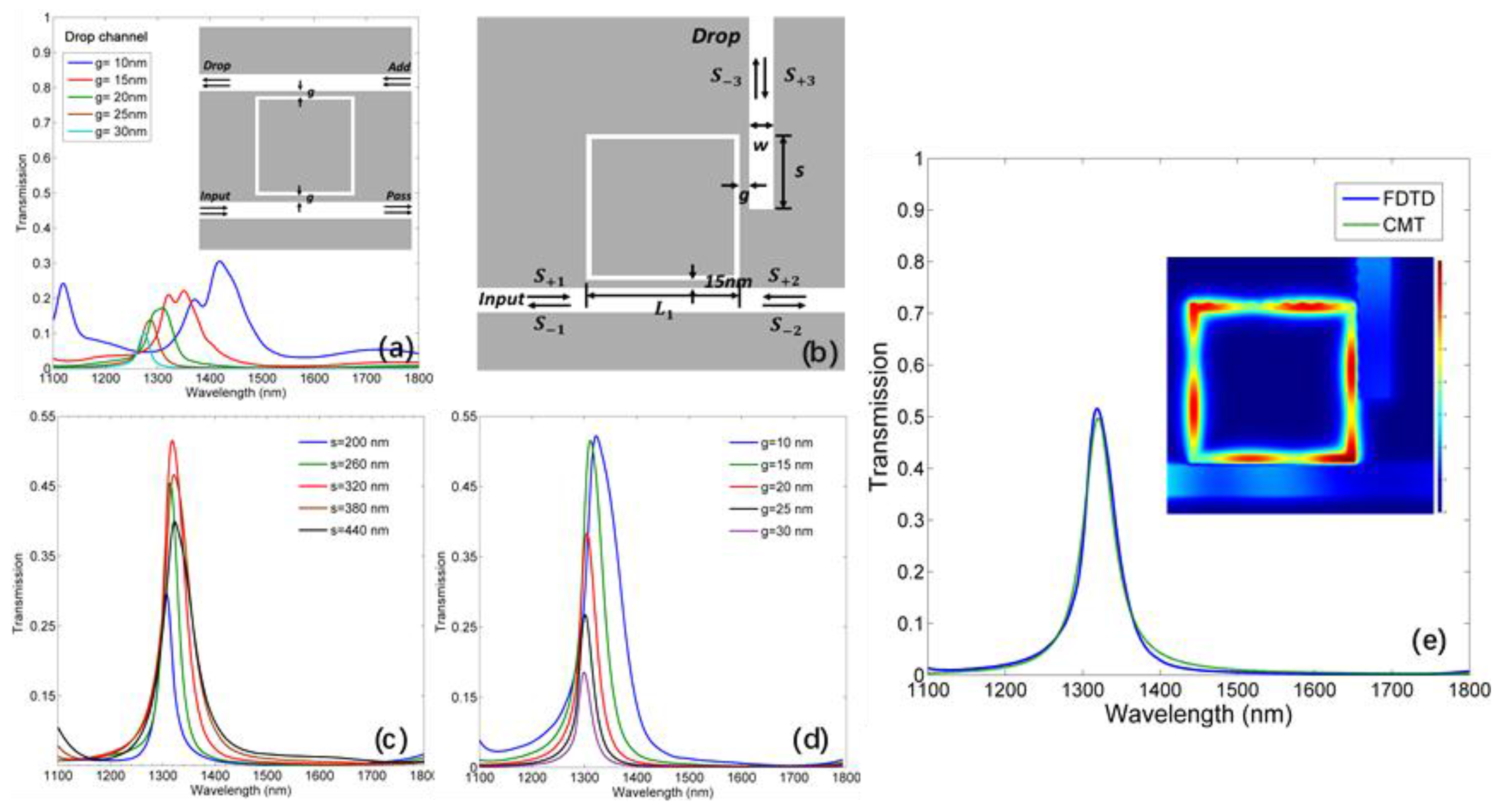
However, when the SRR comes to the traditional add-drop structure, the drop performance is terrible, as shown in Figure 2a. Therefore, we introduce a unique side-coupling method as presented in Figure 2b. The drop waveguide is side-coupled in such a way for two reasons. First, the position of the drop waveguide is selected according to the local mode distribution in the SRR. Besides, since the resonant wave propagates anticlockwise in the SRR, the drop wave will have a shorter optical path by this method than the traditional add-drop coupling way, consequently suffering less from ohmic loss.
The influence of the gap g between the drop waveguide and the SRR on the drop efficiency is studied with s = 320   nm . As given in Figure 2d, the increase of g will cause the decrease of the transmission peak and bandwidth, but the FWHM is lower. Moreover, there is a blue-shift of the transmitted peak wavelength. The effect of the coupling length s on the transmission is also discussed with g = 15   nm . It is shown in Figure 2c that there is an optimum coupling length, s = 320   nm , to achieve the best drop efficiency. According to the inset of Figure 2e, the optimum coupling length is dependent on the mode distribution of the resonant wavelength at the SRR edge adjacent to the drop waveguide. After the optimization of structural parameters, the final result from FDTD is shown in Figure 2e. The drop efficiency at 1310 nm, defined as the ratio of drop to input power, is approximately 52%, and the corresponding FWHM is 45 nm.
The physical mechanism of such a channel drop filter can be theoretically analyzed by CMT [30]. The normalized field amplitude a of the SRR mode can be described as:
d a d t = j ω o a ( 2 τ b + 1 τ b + 1 τ 0 ) a + e j θ 1 2 τ b S + 1 + e j θ 2 2 τ b S + 2 + e j θ 3 2 τ d S + 3
Here, ω 0 refers to the resonant frequency, and 1 / τ b and 1 / τ d represent the decay rates inside the bus and drop waveguide, respectively. 1 / τ 0 is the decay rate due to the ohmic loss of the plasmonic system. S + i and S i (i = 1, 2, 3) represent the normalized amplitudes of input and output SPPs, respectively, as demonstrated in Figure 2b. θ k   ( k = 1 ,   2 ,   3 ) are the phases of the corresponding coupling coefficients. If the reference plane is set at the center of the SRR, there will be θ 1 = θ 2 . According to the power conservation and the time reversal symmetry, we can obtain:
S 1 = S + 2 e j θ 1 2 τ b a S 2 = S + 1 e j θ 1 2 τ b a S 3 = S + 3 + e j θ 3 2 τ d a
In this case, S + 2 = S + 3 = 0 . Therefore, the transmission from the input to the drop channel can be expressed as:
T ( ω ) = | S ˜ 3 S ˜ + 1 | 2 = | e j ( θ 1 θ 3 ) 2 τ b 2 τ d j ( ω ω 0 ) + 2 τ b + 1 τ d + 1 τ 0 | 2
Here, S ˜ represents the Fourier transform of S. The transmission data from CMT is also plotted in Figure 2e, which is in great agreement with the simulated result.
Furthermore, if a reflector structure is utilized at the end of the bus waveguide, the drop efficiency can be improved at the cost of a wider FWHM, as presented in Figure 3a. Consequently, there is a trade-off between the transmission and FWHM. The phase shift of the SPPs when reflected back to the SRR by the reflector can be given by [7]:
ϕ = 4 π Re ( n e f f ) l λ + σ
where σ indicates the phase shift that occurs when reflected back by the metal surface, and l refers to the distance between the reflector surface and the SRR. Obviously, for a particular wavelength we can obtain a ϕ to indicate the incident light and reflected light constructive interfered by changing l . From FDTD, the drop efficiency at 1310 nm can be enhanced to 64% when l = 34 nm, but the FWHM is also improved to 67 nm, as given in Figure 3b. This outcome is comparable with some previous works [4,5,6,7,8,9]. A monitor is set behind the source to detect the reflection, showing that the reflection is only approximately 3% at the drop wavelength, as depicted in Figure 3b. Therefore, the rest of the energy is dissipated due to ohmic loss. Such intrinsic loss is normal and acceptable for an MIM system [3].
According to CMT, there will also be S + 3 = 0 , but S + 2 = e j ϕ S 2 . The transmission will be as follows:
T ( ω ) = | e j ( θ 1 θ 3 ) 2 τ b 2 τ d ( 1 + e j ϕ ) j ( ω ω 0 ) + 2 τ b ( 1 + e j ϕ ) + 1 τ d + 1 τ 0 | 2
The corresponding CMT transmission data is also shown in Figure 3b, and the theory and FDTD results are fitted well.

3. Applications in Sensing and Switching

We choose the structure corresponding to Figure 3b to discuss the following applications. Since the ring resonator is sensitive to ambient RI, such a channel drop filter can be applied to on-chip sensing. The sensing performance can be assessed by two factors [14]:
S = Δ λ Δ n F O M = S F W H M
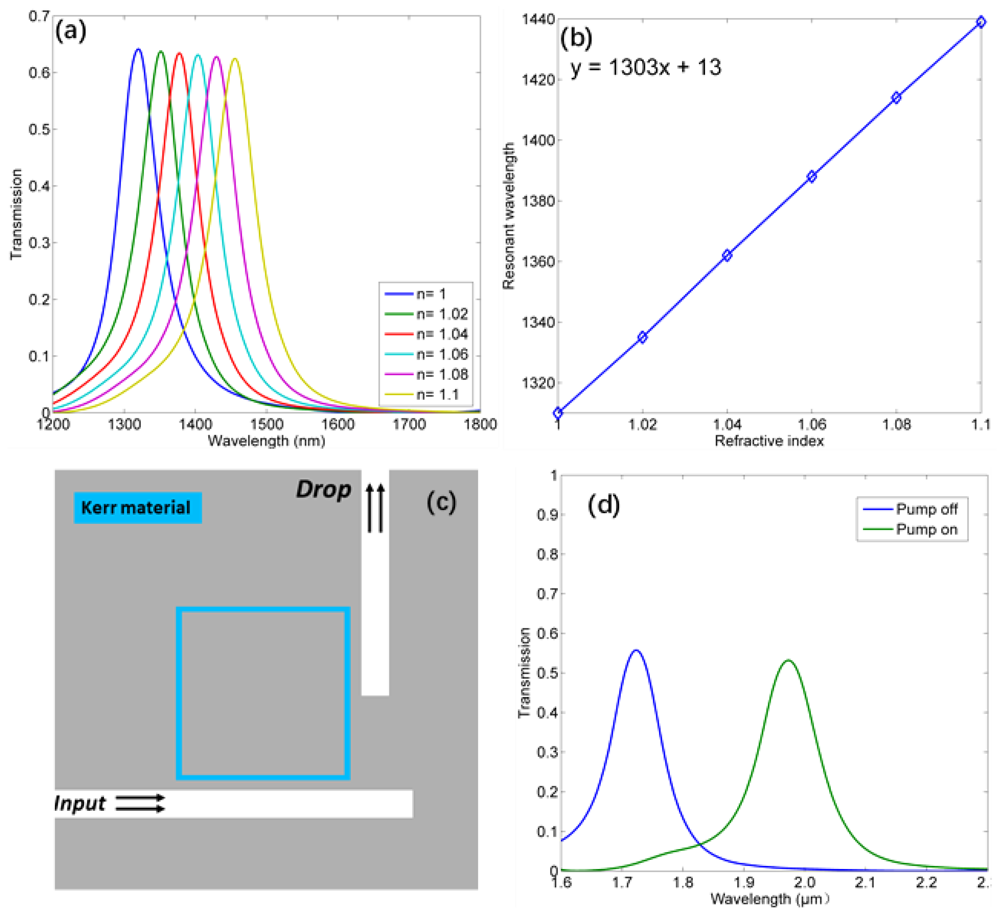
where S is the sensitivity defined as the peak wavelength shift per unit ambient RI, and the figure of merit (FOM) represents the resolution of such a shift. Figure 4a shows the drop wavelength shift with different ambient RI values. This structure has a high sensitivity up to 1303 nm/RIU, as indicated in Figure 4b, which can meet the requirement of chemical-sensing [31]. Besides, the sensitivity can be easily enhanced by increasing the side length of the SRR [14]. Since the FWHM is 67 nm, the FOM is approximately 20/RIU. This value is better than those reported in some recent works based on MIM structures [15,16,17,18,19].
A dynamically tunable device can also be realized based on such a filter filled with nonlinear optical materials, as proposed in Figure 4c. Here we apply nonlinear polymer Kerr material, the RI of which depends on the pump light: n = n 0 + n 2 I , where I is the pump intensity, n 0 is the linear RI, and n 2 is the nonlinear RI. In this case, n 0 = 1.3 and n 2 = 2.87 × 10 8   cm 2 / W [24]. The pump beam can be input from the top (Z axis direction) of this device [12]. Figure 4d shows that optical switching can be achieved at 1.97 μm. With no pump light, the drop efficiency at 1.97 μm is 0.7%, corresponding to the OFF state. After applying the pump light with 6.62   MW / cm 2 , the drop efficiency can be enhanced to 53%, which is the ON state. Such pump intensity is easy to reach in practical experiments [32]. The modulation depth M is defined as [12]:
M = 10 lg T ( I o n ) T ( I o f f )
where T ( I o n ) and T ( I o f f ) are the transmissions corresponding to the ON and OFF states at the modulated wavelength, respectively. In this work, M = 18.8 dB, which is comparable with some previous similar works [10,11,12,13].

4. Dual Demultiplexer for Telecommunication Wavelengths

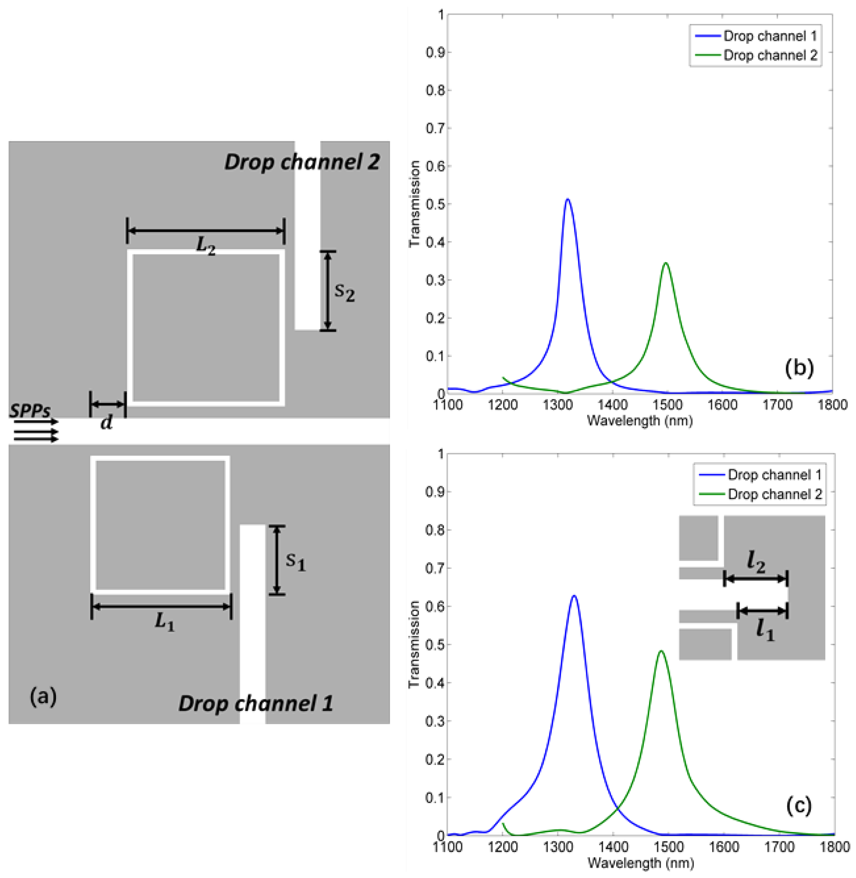
As the upstream and downstream traffic in ethernet passive optical network (EPON), 1310 nm and 1490 nm are two basic telecommunication wavelengths in present fiber-to-the-home (FTTH) systems [33]. Wavelength division multiplex (WDM) work plays an important role in FTTH systems [34], and plasmonic WDM with ultra-small footprints meets the requirement of future highly integrated and more compact all-optical circuits. Here, the plasmonic dual wavelength demultiplexer is introduced, as shown in Figure 5a. Figure 5b is the drop spectrum for two channels; channel 1 for 1310 nm and channel 2 for 1490 nm. The performance of a waveguide demultiplexer can be assessed by two factors; insertion loss (IL) and cross talk (CT) [35]:
I L = 10 lg ( P ω / P i ) C T = 10 lg ( P ω / P u ω )
where P i is the power in the input waveguide, and P ω and P u ω represent the drop powers of the desirable and undesirable wavelengths in one channel, respectively. For channel 1 of this structure, IL = 2.9 dB and CT = 22.8 dB. For channel 2, IL = 4.6 dB and CT = 20.6 dB.
If the reflector is applied, as shown in Figure 5c, the drop efficiencies will be enhanced, and the corresponding parameters will be: IL = 2.0 dB and CT = 23.2 dB for channel 1; IL = 3.2 dB and CT = 18.0 dB for channel 2. Compared with previous works [7,8,9], this device has comparable performance. Furthermore, it makes possible the application of ring resonators on plasmonic integrated wavelength division multiplex (WDM) systems, which is valuable for designing on-chip integrated circuits.

5. Conclusions

In summary, by introducing a special side-coupling method, this work found a way to propose a channel drop filter with the SRR based on the plasmonic MIM structure. This filter not only possesses potential for applications in sensing and switching, but can also be integrated in WDM systems. The CMT is demonstrated to explain the corresponding physical phenomenon in theory. This work will promote future designs based on MIM circuits. Utilizing the characteristics of the ring resonator, this structure can be adapted to more applications, such as on-chip thermometers and slow light.

Acknowledgments

This work is supported by the National Natural Science Foundation of China (60907003, 61671455), the Foundation of NUDT (JC13-02-13, ZK17-03-01), the Hunan Provincial Natural Science Foundation of China (13JJ3001), and the Program for New Century Excellent Talents in University (NCET-12-0142).

Author Contributions

Zhaojian Zhang designed the simulations and wrote the paper; Junbo Yang discussed and revised the paper; Xin He, Yunxin Han, Jingjing Zhang, Jie Huang, and Dingbo Chen gave some advice.

Conflicts of Interest

The authors declare no conflict of interest.

References

  1. Bozhevolnyi, S.I.; Volkov, V.S.; Devaux, E.; Laluet, J.Y.; Ebbesen, T.W. Channel plasmon subwavelength waveguide components including interferometers and ring resonators. Nature 2006, 440, 508–511. [Google Scholar] [CrossRef] [PubMed]
  2. Maier, S.A. Plasmonics: Fundamentals and Applications; Springer: Berlin, Germany, 2014; Volume 52, pp. 49–74. [Google Scholar]
  3. Gramotnev, D.K.; Bozhevolnyi, S.I. Plasmonics beyond the diffraction limit. Nat. Photonics 2010, 4, 83–91. [Google Scholar] [CrossRef]
  4. Zhang, Q.; Huang, X.G.; Lin, X.S.; Tao, J.; Jin, X.P. A subwavelength coupler-type MIM optical filter. Opt. Express 2009, 17, 7549–7554. [Google Scholar] [CrossRef]
  5. Zhang, Z.; Shi, F.; Chen, Y. Tunable multichannel plasmonic filter based on coupling-induced mode splitting. Plasmonics 2015, 10, 139–144. [Google Scholar] [CrossRef]
  6. Xiao, S.; Liu, L.; Qiu, M. Resonator channel drop filters in a plasmon-polaritons metal. Opt. Express 2006, 14, 2932–2937. [Google Scholar] [CrossRef] [PubMed]
  7. Lu, H.; Liu, X.; Gong, Y.; Mao, D.; Wang, G. Analysis of nanoplasmonic wavelength demultiplexing based on metal-insulator-metal waveguides. J. Opt. Soc. Am. B 2011, 28, 1616–1621. [Google Scholar] [CrossRef]
  8. Hu, F.; Yi, H.; Zhou, Z. Wavelength demultiplexing structure based on arrayed plasmonic slot cavities. Opt. Lett. 2011, 36, 1500–1502. [Google Scholar] [CrossRef] [PubMed]
  9. Geng, X.M.; Wang, T.J.; Yang, D.Q.; He, L.Y.; Wang, C. Tunable plasmonic wavelength demultiplexing device using coupled resonator system. IEEE Photonics J. 2016, 8, 1–8. [Google Scholar] [CrossRef]
  10. Taheri, A.N.; Kaatuzian, H. Design and simulation of a nanoscale electro-plasmonic 1 × 2 switch based on asymmetric metal-insulator-metal stub filters. Appl. Opt. 2014, 53, 6546–6553. [Google Scholar] [CrossRef] [PubMed]
  11. He, Z.; Li, H.; Zhan, S.; Li, B.; Chen, Z.; Xu, H. Tunable multi-switching in plasmonic waveguide with Kerr nonlinear resonator. Sci. Rep. 2015, 5, 15837. [Google Scholar] [CrossRef] [PubMed]
  12. Shahamat, Y.; Vahedi, M. Plasmon-induced transparency in a rectangle cavity and an h-shaped structure for sensing and switching applications. J. Nanophotonics 2017, 11, 046012. [Google Scholar] [CrossRef]
  13. Lu, H.; Liu, X.; Wang, L.; Gong, Y.; Mao, D. Ultrafast all-optical switching in nanoplasmonic waveguide with kerr nonlinear resonator. Opt. Express 2011, 19, 2910–2915. [Google Scholar] [CrossRef] [PubMed]
  14. Zhang, Z.; Yang, J.; He, X.; Zhang, J.; Huang, J.; Chen, D.; Han, Y. Plasmonic refractive index sensor with high figure of merit based on concentric-rings resonator. Sensors 2018, 18, 116. [Google Scholar] [CrossRef] [PubMed]
  15. Li, X.; Wei, Z.; Liu, Y.; Zhong, N.; Tan, X.; Shi, S.; Liu, H.; Liang, R. Analogy of electromagnetically induced transparency in plasmonic nanodisk with a square ring resonator. Phys. Lett. A 2016, 380, 232–237. [Google Scholar] [CrossRef]
  16. Yan, S.; Zhang, M.; Zhao, X.; Zhang, Y.; Wang, J.; Jin, W. Refractive index sensor based on a metal–insulator–metal waveguide coupled with a symmetric structure. Sensors 2017, 17, 2879. [Google Scholar] [CrossRef] [PubMed]
  17. Kong, Y.; Wei, Q.; Liu, C.; Wang, S. Nanoscale temperature sensor based on Fano resonance in metal–insulator–metal waveguide. Opt. Commun. 2017, 384, 85–88. [Google Scholar] [CrossRef]
  18. Zhang, X.; Shao, M.; Zeng, X. High quality plasmonic sensors based on Fano resonances created through cascading double asymmetric cavities. Sensors 2016, 16, 1730. [Google Scholar] [CrossRef] [PubMed]
  19. Zhang, Z.; Liang, L.; Xue, C.; Zhang, W.; Yan, S. Fano resonance based on metal-insulator-metal waveguide-coupled double rectangular cavities for plasmonic nanosensors. Sensors 2016, 16, 642. [Google Scholar] [CrossRef] [PubMed]
  20. Chu, H.S.; Akimov, Y.; Bai, P.; Li, E.P. Submicrometer radius and highly confined plasmonic ring resonator filters based on hybrid metal-oxide-semiconductor waveguide. Opt. Lett. 2012, 37, 4564–4566. [Google Scholar] [CrossRef] [PubMed]
  21. Hosseini, A.; Massoud, Y. Nanoscale surface plasmon based resonator using rectangular geometry. Appl. Phys. Lett. 2007, 90, 181102. [Google Scholar] [CrossRef]
  22. Peng, X.; Li, H.; Wu, C.; Cao, G.; Liu, Z. Research on transmission characteristics of aperture-coupled square-ring resonator-based filter. Opt. Commun. 2013, 294, 368–371. [Google Scholar] [CrossRef]
  23. Yan, Y.L.; Fu, G.; Zhang, Y.; Gong, S.X.; Chen, X. A simple nanoscale plasmonic square-shaped ring resonator waveguide. Prog. Electromagn. Res. Lett. 2015, 51, 39–45. [Google Scholar] [CrossRef]
  24. Zavvari, M.; Azar, M.T.H.; Arashmehr, A. Tunable band-stop plasmonic filter based on square ring resonators in a metal-insulator-metal structure. J. Mod. Opt. 2017, 64, 2221–2227. [Google Scholar] [CrossRef]
  25. Wang, S.; Li, Y.; Xu, Q.; Li, S. A MIM filter based on a side-coupled crossbeam square-ring resonator. Plasmonics 2016, 11, 1291–1296. [Google Scholar] [CrossRef]
  26. Shen, X.; Wang, Y.; Chen, Q.; Wu, X. Detuned square ring resonators for multiple plasmon-induced transparencies in metal–insulator–metal waveguide. Appl. Phys. Express 2015, 8, 112201. [Google Scholar] [CrossRef]
  27. Wen, K.; Hu, Y.; Chen, L.; Zhou, J.; He, M.; Lei, L.; Wu, Y.; Li, J. Single- and dual-plasmonic induced absorption in a subwavelength end-coupled composite-square cavity. Appl. Opt. 2017, 56, 8372–8377. [Google Scholar] [CrossRef] [PubMed]
  28. Liu, J.; Fang, G.; Zhao, H.; Zhang, Y.; Liu, S. Plasmon flow control at gap waveguide junctions using square ring resonators. J. Phys. D Appl. Phys. 2010, 43, 055103. [Google Scholar] [CrossRef]
  29. Johnson, P.B. Optical constants of the noble metals. Phys. Rev. B 1972, 6, 4370–4379. [Google Scholar] [CrossRef]
  30. Manolatou, C.; Khan, M.J.; Fan, S.; Villeneuve, P.R.; Haus, H.A.; Joannopoulos, J.D. Coupling of modes analysis of resonant channel add-drop filters. IEEE J. Quantum Electron. 2002, 35, 1322–1331. [Google Scholar] [CrossRef]
  31. Valsecchi, C.; Brolo, A.G. Periodic metallic nanostructures as plasmonic chemical sensors. Langmuir 2013, 29, 5638–5649. [Google Scholar] [CrossRef] [PubMed]
  32. Chai, Z.; Hu, X.; Zhu, Y.; Zhang, F.; Yang, H.; Gong, Q. Low-power and ultrafast all-optical tunable plasmon-induced transparency in plasmonic nanostructures. Appl. Phys. Lett. 2013, 102, 201119. [Google Scholar] [CrossRef]
  33. Koonen, T. Fiber to the home/fiber to the premises: What, where, and when? Proc. IEEE 2006, 94, 911–934. [Google Scholar] [CrossRef]
  34. Park, S.J.; Lee, C.H.; Jeong, K.T.; Park, H.J.; Ahn, J.G.; Song, K.H. Fiber-to-the-home services based on wavelength-division-multiplexing passive optical network. J. Light. Technol. 2004, 22, 2582–2591. [Google Scholar] [CrossRef]
  35. Wu, C.T.; Huang, C.C.; Lee, Y.C. Plasmonic wavelength demultiplexer with a ring resonator using high-order resonant modes. Appl. Opt. 2017, 56, 4039–4044. [Google Scholar] [CrossRef] [PubMed]
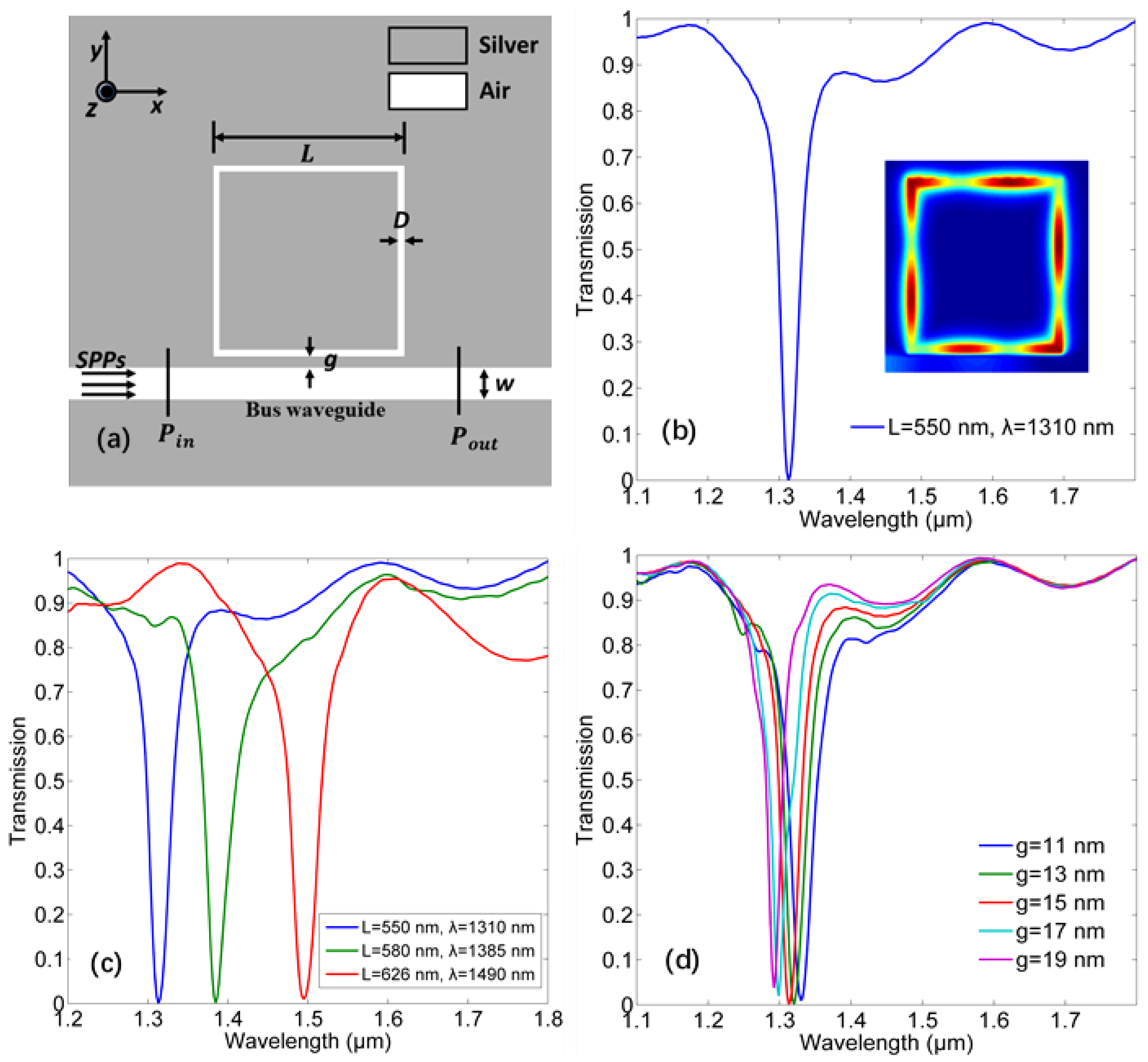
Figure 1. (a) Two-dimensional (2D) structure of the band-stop filter with a single square ring resonator (SRR). L = 550 nm, D = 20 nm, w = 100 nm, g = 15 nm. (b) The transmission spectra of the band-stop filter. The inset is the corresponding field distribution. (c) The transmission spectra pertinent to different side lengths L of the SRR. (d) The transmission spectra pertinent to different gaps g.
Applsci 08 00462 g001
Figure 2. (a) The drop spectrum for the traditional add-drop SRR. (b) The schematic diagram of the band-pass filter. (c) The drop spectrum pertinent to different coupling lengths. (d) The drop spectrum pertinent to different gaps. (e) The transmission spectrum for a channel drop filter with L1 = 546 nm, w = 100 nm, g = 15 nm, s = 320 nm from Finite-Difference Time-Domain (FDTD) and coupled mode theory (CMT). The inset is the field distribution of the channel drop filter.
Applsci 08 00462 g002
Figure 3. (a) The drop spectrum corresponding to different values of l. The inset is the reflector structure. (b) The drop spectrum with a reflector from FDTD and CMT, and the reflection spectrum when l = 34 nm.
Applsci 08 00462 g003
Figure 4. (a) The drop spectrum corresponding to different environmental refractive index (RI) values. (b) The inset is the linear relationship between the drop wavelength and environmental RI. (c) The schematic diagram of the optical switching device. (d) The drop spectrum for optical switching with or without the pump light.
Applsci 08 00462 g004
Figure 5. (a) The schematic diagram of the dual demultiplexer. L1 = 546 nm, L2 = 620 nm, s1 = 320 nm, s2 = 370 nm, g = 15 nm, d = 80 nm. (b) The drop spectrum of channels 1 and 2 without a reflector. (c) The drop spectrum of channels 1 and 2 with a reflector. The inset is the reflector, l1 = 34 nm, l2 = 46 nm.
Applsci 08 00462 g005