Article

Fabrication and Photo-Detecting Performance of 2D ZnO Inverse Opal Films

Department of Materials Science and State Key Laboratory of Molecular Engineering of Polymers, Fudan University, Shanghai 200433, China
*
Author to whom correspondence should be addressed.
Appl. Sci. 2016, 6(10), 259; https://doi.org/10.3390/app6100259
Submission received: 6 June 2016 / Revised: 14 August 2016 / Accepted: 7 September 2016 / Published: 26 September 2016

Abstract

:
Two-dimensional (2D) ZnO inverse opal (IO) films were fabricated by co-assembly of sacrificed polystyrene (PS) microspheres and citric acid/zinc acetate (CA/ZA) aqueous solution at an oil–water interface followed by calcination. Their morphologies could be controlled by the surface property of polymer templates and CA/ZA molar ratio. Moreover, photo-detecting devices based on such films were constructed, which showed high photocurrent (up to 4.6 μA), excellent spectral selectivity, and reversible response to optical switch.

1. Introduction

Two-dimensional (2D) inverse opals (IOs) with periodical porous structures always have large surface area and unique optical properties [1]. Therefore, they have demonstrated great potential in a variety of application fields, such as sensors, light-emitting diodes (LEDs), electrochromic devices, and surface-enhanced Raman spectroscopy (SERS) [2,3,4,5].
Basically, fabrication of 2D IOs often requires multiple steps: (1) formation of a monolayer colloidal crystal (MCC) template film; (2) infiltration of precursors or matrix materials into the voids of the template film; (3) removal of the colloidal templates by dissolution or calcination. As recently reviewed in detail by Jonas et al. [6], MCC templates can be achieved by a variety of methods, including dip-coating, spin-coating, slope self-assembly, etc. [7,8,9,10,11,12]. Regarding infiltration and replication strategies, evaporation deposition, electrochemical deposition, and solution/sol-based infiltration methods are mainly included [13,14,15]. Among them, the solution/sol based method has been widely used for its advantages: low-cost, simplicity, and versatility. To date, 2D IOs with various chemical compositions, including Ag, In2O3, ZnO, CeO2, Fe2O3, etc. have been successfully achieved through this method [5,16,17]. However, there still remain some problems to be solved. For instance, poor regularity and cracks may arise from the infiltration step or the subsequent calcination process due to solution flow, shrinkage, or change in surface tension.
In order to overcome these drawbacks, a novel strategy that uses floating MCCs as templates has been developed [4,18,19]. Since template colloids are loosely connected with each other, prior-prepared crystalline nanoparticles can be easily introduced into the interstitial spaces without damaging the template. Floating MCCs can also serve as masks for in situ interfacial reaction to fabricate 2D IOs, including PbS, Ag, and CaCO3 nanonets [20].
Oil–water interfacial assembly has been proven to be an effective way of obtaining high-quality floating MCC templates [21]. Very recently, we fabricated NixMg1-xO nanobowl array photo-detecting devices via the oil–water interfacial assembly of polystyrene (PS) colloids and metal oxide precursors, followed by calcination [22]. However, for the device constructed by NixMg1-xO, the photocurrent and selectivity still need to be improved.
Here, we further extend the oil–water interfacial assembly method to fabricate a PS/citric acid (CA)-zinc acetate (ZA) precursor monolayer film, and crack-free 2D ZnO IO films were obtained after calcination of the PS/precursor film. Moreover, photo-detecting devices constructed on such films showed high photocurrent, excellent spectrum selectivity and reversible response to ultraviolet (UV) lights.

2. Materials and Methods

2.1. Materials

Styrene (St), acrylic acid (AA), Poly(vinylpyrrolidone) (PVP, K-30), zinc acetate (ZA), hexane, Citric acid (CA) and ethanol were purchased from Sinopharm Chemical Reagent Co. Ltd. (Shanghai, China). α,α’-azodiisobutyramidine dihydrochloride (AIBA) and potassium persulfate (KPS) were obtained from Aladdin Reagent Corp (Shanghai, China).

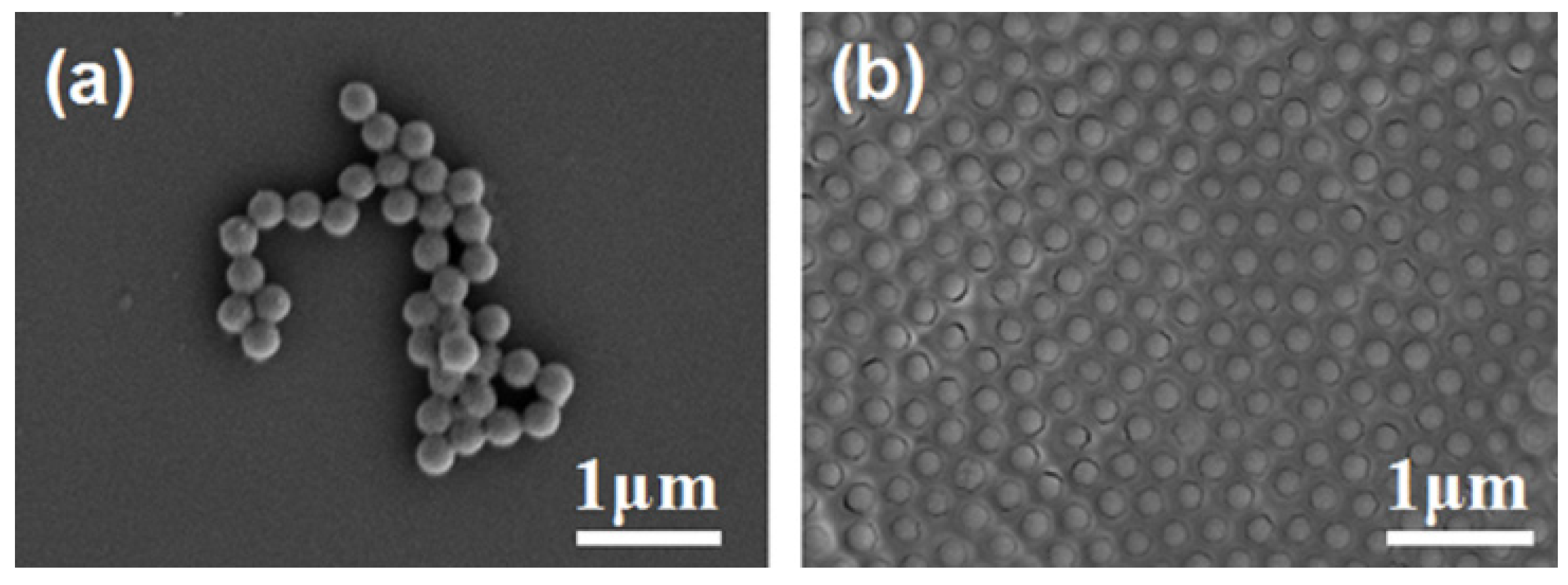
2.2. Synthesis of Monodisperse Polymer Microspheres

Monodisperse PS template microspheres with average diameter of 300 nm were synthesized by emulsion polymerization similar to our previous work [22], as follows: St (10.0 g), PVP (1.0 g), and H2O (90.0 g) were charged into a 250 mL four-neck flask with a temperature controller, a mechanical stirrer, a N2 inlet, and a Graham condenser. The reaction system was stirred at a rate of 200 rpm and deoxygenated by N2 at room temperature for 30 min. Then, it was heated to 75 °C, followed by the addition of initiator solution (0.26 g of AIBA in 10 g of water). After that, the reaction was kept at 75 °C for another 24 h to obtain PS emulsion.
Monodisperse poly(styrene-co-acrylic acid) (PSA) microspheres with average diameter of 200 nm were synthesized by a similar procedure, using the following formulation: St (5 g), AA (0.5 g), H2O (135 g), and KPS solution (0.2 g of KPS in 10 g of H2O) as initiator.

2.3. Co-Assembly of Polymer Microspheres and CA-ZA into Monolayer Film

The monolayer PS/CA-ZA film was obtained via oil–water self-assembly method, as shown in Scheme 1a–c. First, 15 mL of precursor aqueous solution containing 1.1 g of ZA and different amounts of CA (typically 0.23 g for mol ratio of CA/ZA = 0.2:1) was mixed with 5 mL of PS dispersion (0.2 wt %) in a 50 mL beaker. Next, 5 mL of hexane was introduced to produce an oil–water interface. Then, 2 mL of ethanol was slowly added to the interface at a low rate by a syringe (4 mL/h) by a syringe until the interface was completely covered by assembled PS microspheres. After careful removal of most of the hexane at the top by a syringe, the film was laid 30 min for the precursor solution to infiltrate into the voids of the PS microspheres homogeneously. Next, the as-assembled film was transferred to a thermally-oxidized Si substrate by pulling the substrate out of the liquid phase at a slow speed of 1 mm/min using a SYDC-I dip coater (Sanyan instrument Co., Ltd., Shanghai, China). For comparison, PSA microspheres were also assembled into a monolayer film in the same way.

2.4. Fabrication of 2D ZnO Inverse Opal and Photo-Detecting Device

Scheme 1d–e depicts the procedure for the fabrication of 2D ZnO IO film device. After drying in a Petri dish with cover, the as-obtained PS/CA-ZA film was annealed in air from room temperature to 600 °C with a heating speed of 2 °C min−1 and maintained at 600 °C for 2 h. Then, Cr/Au (80 nm/30 nm) electrodes (distance ≈ 25 μm) were deposited on the 2D ZnO IO film by electron beam evaporation (TENSTAR TSV-1300) with the assistance of a metal mask to achieve the photo-detecting device. The current–voltage (I–V) characteristics of the IO ZnO film photodetector were measured using an Advantest Picoammeter R8340A and a DC voltage source R6411. A spectral response for different wavelengths was recorded by using a xenon lamp (500 W).

2.5. Characterization

The morphologies of the films were characterized by a field emission scanning electron microscope (SEM, Zeiss Ultra 55, Oberkochen, Germany) at 2 kV. The crystal structures of the annealed ZnO powder derived from the corresponding PS/CA-ZA dispersion were investigated via X-ray diffraction (XRD, Bruker D8 Advance) using Cu Kα radiation (λ = 0.15418 nm). High resolution transmission electron microscopy (HRTEM) images and selective area electron diffraction (SAED) patterns of the particles scraped from the the 2D ZnO IO film were obtained using a HRTEM (Tecnai G2F 20 S-Twin, FEI, Hillsboro, OR, USA) operating at 200 keV. A UV-Vis spectrophotometer (Hitachi U-4100, Hitachi, Japan) was used to record the absorbance of the 2D ZnO inverse opal films fabricated on quartz substrates. The current–voltage (I–V) characteristics and time-dependent on/off characteristics of the film devices were measured by a picoammeter (Keithley 4200-SCS, Keithley, Beaverton, OR, USA).

3. Results and Discussion

3.1. Fabrication of Monolayer Polymer/CA-ZA Film

The PS template microspheres were assembled at the oil–water interface in the presence of CA-ZA solution as follows: when the inducer (ethanol) was added to the oil–water interface, the PS microspheres readily assembled into a mirror-like monolayer film at the oil–water interface, which contributed to the reduction in the total interfacial energy [23]. The as-formed film was easily transferred to a SiO2/Si substrate by scooping.
Both PS and PSA microspheres were tried to self-assemble at the oil–water interfaces, respectively, in the presence of CA-ZA aqueous solution. Figure 1 shows the SEM images of co-assembly results when using PSA microspheres (200 nm in diameter) as templates. If the self-assembly process was carried out in the presence of ZA without CA, few PSA microspheres floated to the interface and PSA templates dispersed in the sub-phase began to aggregate within just 30 min (Figure 1a). However, in a CA-ZA solution with the molar ratio of 1:1, PSA microspheres were stable enough to form a close-packed monolayer (Figure 1b). On the other hand, Figure 2 reveals that PS microspheres (300 nm in diameter) could self-assemble into an ordered monolayer film in a large area with very few defects at various CA/ZA molar ratios. These results demonstrated that both the surface property of polymer microspheres and the CA/ZA molar ratio have a great impact on the morphology of the PS/precursor film, which could be explained as follows: good dispersion without the aggregation of template colloids is the prerequisite to obtain an ordered monolayer particle film. So, we speculate that the strong electrostatic interaction between Zn2+ and carboxylic groups (–COOH) on PSA may cause aggregation among microspheres, thus inhibiting the co-assembly process. If Zn2+ is complexed with CA, the electrostatic interaction can be eliminated. For this reason, PS microspheres were used as templates to self-assemble into a monolayer film in the following experiments.

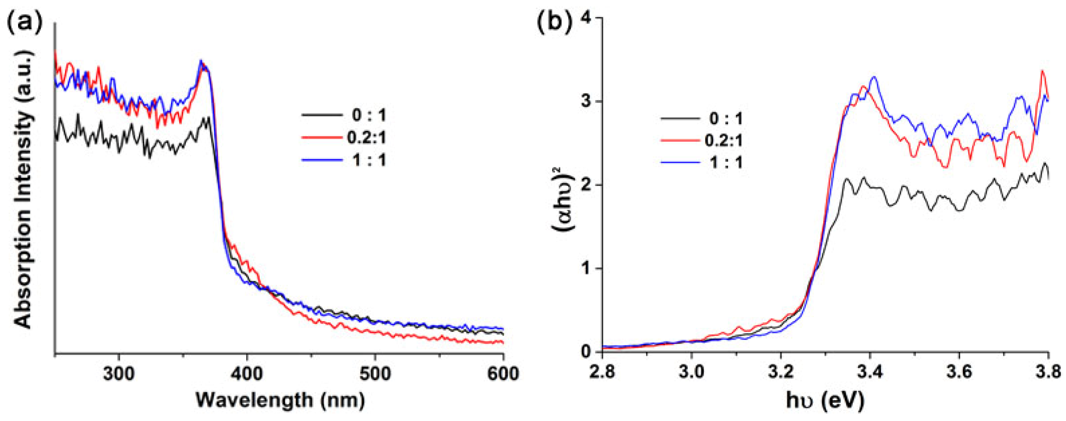
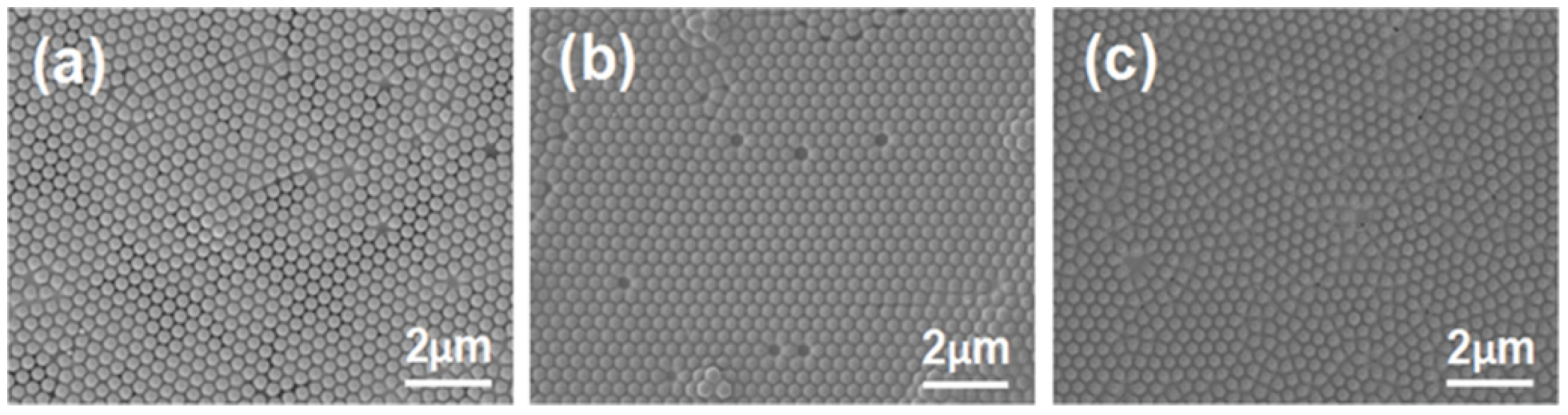
3.2. Fabrication and Characterization of 2D ZnO IO Films

The as-prepared monolayer PS/CA-ZA films were further annealed in air to remove the PS templates, hence obtaining 2D ZnO IO films. Figure 3 shows the SEM images of the 2D ZnO IO films fabricated at different CA/ZA molar ratios. From Figure 3a,b one can see that the IO film fabricated without CA had rough walls and a broken bottom; cracks across the film indicate poor connectivity. In contrast, when the molar ratio of CA/ZA was 0.2:1, the 2D ZnO IO film had thinner walls and a continuous bottom, despite of some holes (Figure 4c,d). The inner pore size was calculated to be about 280 nm, slightly smaller than the diameter of template microspheres, which may be due to framework shrinkage during the calcination process. When the CA/ZA molar ratio further increased to 1:1, a film with rough walls and a continuous bottom was obtained (Figure 4e,f). In this work, CA was used as a complexing agent to form homogeneous precursor gel with ZA, which “glues” PS microspheres together to yield crack-free IOs [24]. Similar results were reported in a previous study [25]. The gelation during drying also narrows the gaps between PS microspheres, and the addition of CA may provide a better adhesion to the substrate. As a result, more ZnO nanoparticles grow from the substrate rather than interstices between PS microspheres with increasing CA/ZA molar ratio.
Figure 4 shows the XRD spectra of annealed ZnO powder at different CA/ZA molar ratios. All of the peaks can be indexed to the (100), (002), (101), (102), (110), (103), (200), (112), (201), (004), and (202) planes of hexagonal wurtzite ZnO structure according to JCPDS No. 36-1451. These results indicate that the films fabricated at different CA/ZA molar ratios have the same crystal structure as hexagonal wurtzite ZnO.
To further confirm the microstructure of the 2D ZnO IO film, HRTEM and SAED patterns were used to examine the ZnO nanoparticles taken from the film with the CA/ZA molar ratio of 1:1. Figure 5b shows the HRTEM image of the nanoparticles scraped from the film. The interplanar distances of 0.25 nm and 0.26 nm are attributed to the (101) and (002) planes of hexagonal wurtzite ZnO, respectively. The SAED pattern shows seven diffraction rings corresponding to (100), (002), (101), (102), (110), (103), and (200) planes of hexagonal wurtzite ZnO (Figure 5c). These results also reveal the polycrystalline wurtzite ZnO structure of the film.
Figure 6a shows the UV-Vis absorbance spectrums of the 2D ZnO IO films with different CA/ZA molar ratios. All films are highly transparent in the visible region and have strong UV absorption below 370 nm. Their bandgaps can be estimated by the following equation:
(αhν)2 = C(hνEg),
where α is the absorption coefficient, hν is the light energy, C is a constant, and Eg is the band gap energy [26]. Figure 6b shows the corresponding (αhν)2-hν curves. The bandgaps are estimated to be 3.25, 3.25, and 3.22 eV when the CA/ZA molar ratios are 0:1, 0.2:1, and 1:1, respectively. There is little change in bandgap despite differences in the CA/ZA molar ratio.

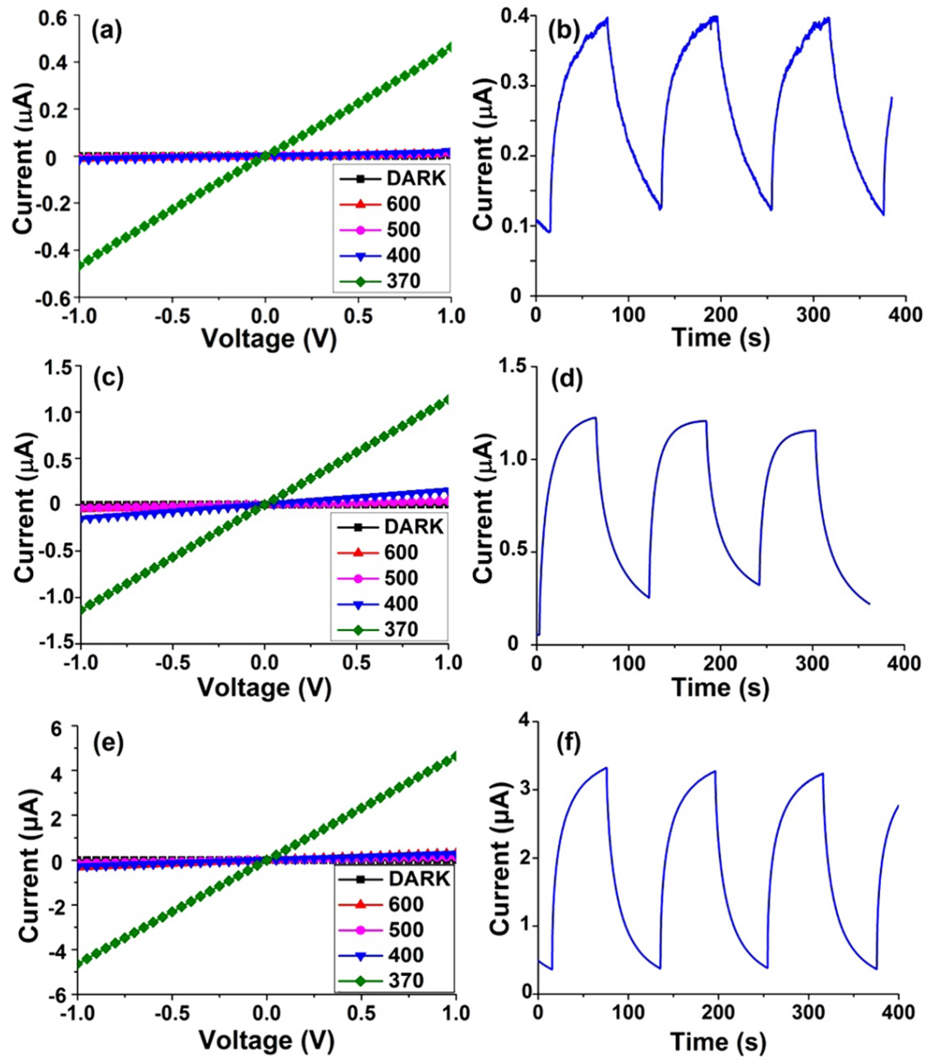
3.3. Photo-Detecting Properties of 2D ZnO IO Film Devices

IO film-based photodetectors were further constructed by depositing Cr/Au (80 nm/30 nm) electrodes on the as-obtained 2D ZnO IO films. Figure 7 shows the current–voltage (I–V) curves and time-dependent response of the devices. The I–V curves were measured at bias from −1 to 1 V under dark conditions, 600 nm (1.16 mW·cm−2), 500 nm (2.30 mW·cm−2), 400 nm (2.37 mW·cm−2), and 370 nm (2.12 mW·cm−2) illumination. The linear I–V characteristics indicate good Ohmic contacts between films and electrodes. All samples showed no obvious change of current under dark condition and visible light (600, 500, and 400 nm), while the photocurrent increased dramatically under 370 nm illumination. This presents good spectral selectivity of these 2D ZnO IO film devices. As reported in previous study, the enhancement in photocurrent can be explained by an increase in the excited electron-hole pairs and a decrease in the width of the oxygen depletion layer when the device is illuminated by light of an energy above the threshold excitation energy of ZnO [27]. Time-dependent on/off characteristic measurements were carried out under 370 nm illumination at a bias of 1 V with an on/off internal of 1 min. It was shown that the devices can be switched reversibly between on and off states.
The detailed performances of the IO film-based photodetectors are listed in Table 1. The photocurrent becomes higher with the increase of the CA/ZA molar ratio. When the CA/ZA molar ratio is 1:1, the as-prepared device has the largest photocurrent and UV/dark current (Ip/Id) ratio up to 4.6 μA and 1917, respectively. Many factors, such as crystallite orientations, crystallite sizes, porous microstructures, and film thickness may influence the photoresponse characteristics [28]. There are probably two reasons for the enhancement in photocurrent when increasing CA/ZA ratio in this study. On one hand, the crack-free 2D ZnO IO nanofilms fabricated with the addition of CA have better connectivity and larger coverage on the substrate, thus causing stronger UV absorption than the broken one fabricated without CA. On the other hand, photocurrent may also increase with the grain size [29]. Since the nanofilms fabricated with the CA/ZA ratios of 0.2:1 and 1:1 have similar coverage and UV absorption, the increase in photocurrent probably comes from their rougher bottom with larger grain size. Table 2 summaries a comparison of the photoconduction properties based on the present ZnO IO film with other ZnO nanostructures, including nanoparticles [30] and hollow-sphere nanofilm [27]. These key parameters are comparable to or better than those of other ZnO nanostructures with different shapes.

4. Conclusions

An oil–water interfacial co-assembly method was used to fabricate 2D crack-free ZnO IO nanofilms, in which the assembly of PS template colloids and infiltration of Zn2+ ions were carried out simultaneously. The morphologies of 2D ZnO IO nanofilms varied with the CA/ZA molar ratio. Photo-detecting devices based on such nanofilms showed excellent selectivity and reversible response to optical switch. When the CA/ZA molar ratio was 1:1, the nanofilm device exhibited the largest photocurrent up to 4.6 μA at 1 V bias, which was 1917 times that of the dark current. In this way, this type of crack-free 2D IO film-based device has great potential in high-performance photodetectors, optoelectronic switches, and solar cells.

Acknowledgments

Financial supports of this research from the National Natural Science Foundation of China (51322307, 51273218), and “Shu Guang” project supported by Shanghai Municipal Education Commission and Shanghai Education Development Foundation are appreciated.

Author Contributions

Xin Lin and Min Chen conceived and designed the experiments; Xin Lin performed the experiments; Xin Lin and Min Chen analyzed the data; Xin Lin and Min Chen wrote the paper.

Conflicts of Interest

The authors declare no conflict of interest.

References

  1. Li, Y.; Cai, W.P.; Duan, G.T. Ordered micro/nanostructured arrays based on the monolayer colloidal crystals. Chem. Mater. 2008, 20, 615–624. [Google Scholar] [CrossRef]
  2. Ye, X.Z.; Li, Y.; Dong, J.Y.; Xiao, J.Y.; Ma, Y.R.; Qi, L.M. Facile synthesis of ZnS Nanobowl arrays and their applications as 2D photonic crystal sensors. J. Mater. Chem. C 2013, 1, 6112–6119. [Google Scholar] [CrossRef]
  3. Hyun, W.J.; Lee, H.K.; Oh, S.S.; Hess, O.; Choi, C.G.; Im, S.H.; Park, O.O. Two-Dimensional TiO2 Inverse Opal with a closed top surface structure for enhanced light extraction from polymer light-emitting diodes. Adv. Mater. 2011, 23, 1846–1850. [Google Scholar] [CrossRef] [PubMed]
  4. Li, H.; Theriault, J.; Rousselle, B.; Subramanian, B.; Robichaud, J.; Djaoued, Y. Facile fabrication of crack-free large-area 2D WO3 Inverse Opal films by a ‘dynamic hard-template’ strategy on ITO substrates. Chem. Commun. 2014, 50, 2184–2186. [Google Scholar] [CrossRef] [PubMed]
  5. He, L.F.; Huang, J.A.; Xu, T.T.; Chen, L.M.; Zhang, K.; Han, S.T.; He, Y.; Lee, S.T. Silver nanosheet-coated Inverse Opal film as a highly active and uniform SERS substrate. J. Mater. Chem. 2012, 22, 1370–1374. [Google Scholar] [CrossRef]
  6. Vogel, N.; Retsch, M.; Fustin, C.A.; Jonas, U. Advances in colloidal assembly: The design of structure and hierarchy in two and three dimensions. Chem. Rev. 2015, 115, 6265–6631. [Google Scholar] [CrossRef] [PubMed]
  7. Ye, X.Z.; Qi, L.M. Recent advances in fabrication of monolayer colloidal crystals and their inverse replicas. Sci. China Chem. 2014, 57, 58–69. [Google Scholar] [CrossRef]
  8. Retsch, M.; Zhou, Z.C.; Rivera, C.; Kappl, M.; Zhao, X.S.; Jonas, U.; Li, Q. Fabrication of large-area, transferable colloidal monolayers utilizing self-assembly at the air/water interface. Macromol. Chem. Phys. 2009, 210, 230–241. [Google Scholar] [CrossRef]
  9. Vogel, N.; Viguerie, L.; Jonas, U.; Weiss, C.K.; Landfester, K. Wafer-Scale fabrication of ordered binary colloidal monolayers with adjustable stoichiometries. Adv. Funct. Mater. 2011, 21, 3064–3073. [Google Scholar] [CrossRef]
  10. Wu, Y.Z.; Zhang, C.; Yuan, Y.; Wang, Z.W.; Shao, W.J.; Wang, H.J.; Xu, X.L. Fabrication of wafer-size monolayer close-packed colloidal crystals via slope self-assembly and thermal treatment. Langmuir 2013, 29, 14017–14023. [Google Scholar] [CrossRef] [PubMed]
  11. Moon, G.D.; Lee, T.I.; Kim, B.; Chae, G.S.; Kim, J.; Kim, S.H.; Myoung, J.M.; Jeong, U. Assembled monolayers of hydrophilic particles on water surfaces. ACS Nano 2011, 5, 8600–8612. [Google Scholar] [CrossRef] [PubMed]
  12. Xiong, S.S.; Dunphy, D.R.; Wilkinson, D.C.; Jiang, Z.; Strzalka, J.; Wang, J.; Su, Y.; de Pablo, J.J.; Brinker, C.J. Revealing the interfacial self-assembly pathway of large-scale, highly-ordered, nanoparticle/polymer monolayer arrays at an air/water interface. Nano Lett. 2013, 13, 1041–1046. [Google Scholar] [CrossRef] [PubMed]
  13. Yang, J.L.; Duan, G.T.; Cai, W.P. Controllable fabrication and tunable magnetism of nickel nanostructured ordered porous arrays. J. Phys. Chem. C 2009, 113, 3973–3977. [Google Scholar] [CrossRef]
  14. Duan, G.T.; Cai, W.P.; Li, Y.; Li, Z.G.; Cao, B.Q.; Luo, Y.Y. Transferable ordered Ni hollow sphere arrays induced by electrodeposition on colloidal monolayer. J. Phys. Chem. B 2006, 110, 7184–7188. [Google Scholar] [CrossRef] [PubMed]
  15. Li, Y.; Cai, W.P.; Duan, G.T.; Cao, B.Q.; Sun, F.Q.; Lu, F. Superhydrophobicity of 2D ZnO ordered pore arrays formed by solution-dipping template method. J. Colloid Interface Sci. 2005, 287, 634–639. [Google Scholar] [CrossRef] [PubMed]
  16. Li, Y.; Cai, W.P.; Duan, G.T.; Sun, F.Q.; Cao, B.Q.; Lu, F. 2D nanoparticle arrays by partial dissolution of ordered pore films. Mater. Lett. 2005, 59, 276–279. [Google Scholar] [CrossRef]
  17. Sun, F.Q.; Cai, W.P.; Li, Y.; Cao, B.Q.; Lei, Y.; Zhang, L.D. Morphology-controlled growth of large-area two-dimensional ordered pore arrays. Adv. Funct. Mater. 2004, 14, 283–288. [Google Scholar] [CrossRef]
  18. Li, H.; Vienneau, G.; Jones, M.; Subramanian, B.; Robichaud, J.; Djaoued, Y. Crack-Free 2D-Inverse Opal anatase TiO2 films on rigid and flexible transparent conducting substrates: Low temperature large area fabrication and electrochromic properties. J. Mater. Chem. C 2014, 2, 7804–7810. [Google Scholar] [CrossRef]
  19. Zhen, H.Y.; Li, K. A Surfactant-Free Co-Assembly route to fabricate 2D TiO2-WO3 composite Inverse Opal films for photochromic applications. New J. Chem. 2014, 38, 4041–4044. [Google Scholar] [CrossRef]
  20. Li, C.; Hong, G.S.; Qi, L. Nanosphere Lithography at the Gas/Liquid Interface: A General approach toward free-standing high-quality nanonets. Chem. Mater. 2010, 22, 476–481. [Google Scholar] [CrossRef]
  21. Chen, H.; Hu, L.F.; Fang, X.S.; Wu, L.M. General fabrication of monolayer SnO2 nanonets for high-performance ultraviolet photodetectors. Adv. Funct. Mater. 2012, 22, 1229–1235. [Google Scholar] [CrossRef]
  22. Zhao, Y.; Hu, L.F.; Gao, S.P.; Liao, M.Y.; Sang, L.W.; Wu, L.M. One-step self-assembly fabrication of high quality NixMg1-xO bowl-shaped array film and its enhanced photocurrent by Mg2+ doping. Adv. Funct. Mater. 2015, 25, 3256–3263. [Google Scholar] [CrossRef]
  23. Hu, L.F.; Chen, M.; Fang, X.S.; Wu, L.M. Oil-water interfacial self-assembly: A novel strategy for nanofilm and nanodevice fabrication. Chem. Soc. Rev. 2012, 41, 1350–1362. [Google Scholar] [CrossRef] [PubMed]
  24. Mondelaers, D.; Vanhoyland, G.; van den Rul, H.; D’Haen, J.; van Bael, M.K.; Mullens, J.; van Poucke, L.C. Synthesis of ZnO nanopowder via an aqueous acetate-citrate gelation method. Mater. Res. Bull. 2002, 37, 901–914. [Google Scholar] [CrossRef]
  25. Hatton, B.; Mishchenko, L.; Davis, S.; Sandhage, K.H.; Aizenberg, J. Assembly of large-area, highly ordered, Crack-Free Inverse Opal films. Proc. Natl. Acad. Sci. USA 2010, 107, 10354–10359. [Google Scholar] [CrossRef] [PubMed]
  26. Khanlary, M.R.; Isazadeh, S. Structural and optical properties of ZnO thin films prepared by Sol-Gel method. Micro Nano Lett. 2011, 6, 767–769. [Google Scholar] [CrossRef]
  27. Chen, M.; Hu, L.F.; Xu, J.X.; Liao, M.Y.; Wu, L.M.; Fang, X.S. ZnO hollow-sphere nanofilm-based high-performance and low-cost photodetector. Small 2011, 7, 2449–2453. [Google Scholar] [CrossRef] [PubMed]
  28. Ghosh, R.; Mallik, B.; Basak, D. Dependence of photoconductivity on the crystallite orientations and porosity of polycrystalline ZnO films. Appl. Phys. A 2005, 81, 1281–1284. [Google Scholar] [CrossRef]
  29. Kung, S.C.; Xing, W.D.; van der Veer, W.E.; Yang, F.; Donavan, K.C.; Cheng, M.; Hemminger, J.C.; Penner, R.M. Tunable photoconduction sensitivity and bandwidth for lithographically patterned nanocrystalline cadmium selenide nanowires. ACS Nano 2011, 5, 7627–7639. [Google Scholar] [CrossRef] [PubMed]
  30. Jun, J.H.; Seong, H.J.; Cho, K.; Moon, B.M.; Kim, S. Ultraviolet photodetectors based on ZnO nanoparticles. Ceram. Int. 2009, 35, 2797–2801. [Google Scholar] [CrossRef]
Scheme 1. Schematic illustration for the fabrication of two-dimensional (2D) ZnO inverse opal (IO) film and the corresponding photo-detecting device.
Applsci 06 00259 sch001
Figure 1. Scanning electron microscope (SEM) images of the poly(styrene-co-acrylic acid) (PSA) microspheres assembled in (a) zinc acetate (ZA) solution and (b) citric acid-zinc acetate (CA-ZA) solution (CA/ZA molar ratio = 1:1).
Applsci 06 00259 g001
Figure 2. SEM images of polystyrene (PS)/precursor films with different CA/ZA molar ratios: (a) 0:1; (b) 0.2:1; (c) 1:1.
Applsci 06 00259 g002
Figure 3. SEM images of ZnO IO films on SiO2/Si substrates fabricated at different CA/ZA molar ratios: (a,b) 0:1; (c,d) 0.2:1; (e,f) 1:1.
Applsci 06 00259 g003
Figure 4. X-ray diffraction (XRD) spectrums of annealed ZnO powder at different CA/ZA molar ratios: (a) 0:1; (b) 0.2:1; (c) 1:1.
Applsci 06 00259 g004
Figure 5. (a) Transmission electron microscopy (TEM) image; (b) high-resolution TEM (HRTEM) image; and (c) selective area electron diffraction (SAED) pattern of nanoparticles scraped from the 2D ZnO IO film (CA/ZA molar ratio = 1:1).
Applsci 06 00259 g005
Figure 6. (a) Ultraviolet (UV)-Vis absorbance spectrums of the 2D ZnO IO films with different CA/ZA molar ratios; (b) Corresponding (αhν)2-hν curve.
Applsci 06 00259 g006
Figure 7. The current–voltage (I–V) curves and time-dependent response (at 370 nm, 1 V bias) of film devices with different CA/ZA molar ratios: (a,b) 0:1; (c,d) 0.2:1; (e,f) 1:1.
Applsci 06 00259 g007
Table 1. Summary of the ultraviolet (UV) detecting performance of inverse opal (IO) film photodetectors.
CA/ZA c Molar RatioId a (μA)Ip b (μA)Ip/Id
0:19.7 × 10−40.46474
0.2:11.7 × 10−31.1647
1:12.4 × 10−34.61917
a Id: Dark current at 1 V bias; b Ip: Photocurrent at 1 V bias illuminated under 370 nm illumination; c CA/ZA, citric acid/zinc acetate.
Table 2. Representative results of ZnO nanostructures with different shapes, and their corresponding UV photodetector performances. NPs: nanoparticles; HS: hollow-sphere; IO: inverse opal.
NanostructuresLight of DetectionBias (V)Dark CurrentPhoto CurrentReference
NPs325 nm1~0.4 pA0.3 μA[30]
HS350 nm, 1.32 mW·cm250.05 μA2.62 μA[27]
IO370 nm, 2.12 mW·cm−212.4 × 10⁻³ μA4.6 μAThis work

