Abstract
We experimentally demonstrate high-resolution imaging using micro-objectives fabricated by two-photon polymerization (2PP) lithography, highlighting its potential as a flexible and precise fabrication method. The 2PP manufacturing process offers the ability to develop micro-optics with customized geometries and material properties, including tailored refractive indices. This flexibility introduces new degrees of freedom in optical system design and expands the applicability of micro-optics to advanced imaging tasks where other materials and fabrication methods are insufficient. For our study, bi-convex micro-optics with different geometries with radii of curvature of <15 m and minimized contact areas (<1 ) to ensure easy release from the substrate were fabricated with 2PP and investigated for their optical performance. With these micro-optics, the tracks with a pitch of 320 nm and the pits and lands as small as 130 nm were successfully resolved on a BluRay disc surface, demonstrating for the first time the high-resolution imaging capabilities of bi-convex spherical micro lenses.
1. Introduction
The observation of minute objects and their details is an essential basis for research, development, and quality assurance in many areas of scientific investigation, including physics, chemistry, materials science, and life sciences. A robust and simultaneously simple method of observation of such minute objects is provided by light optical microscopy. This method allows for observation of the far field with a single aperture, without the use of additional effects such as fluorescence. However, the resolution limit, first described by Ernst Abbe in 1873 [] and further specified by Lord Rayleigh in 1879 [], represents a physical limitation for the smallest object details that can be resolved. The resolution limit can be attributed to the absence of evanescent waves in the far field. Evanescent waves transmit the high spatial frequency components of the minute details of the object and exponentially decay with distance, rendering them invisible in the far field. Over the decades, various methods have been developed either in the field of near-field microscopy, e.g., scanning near-field optical microscopy (SNOM) [,], or in far-field microscopy [], e.g., stochastic optical reconstruction microscopy (STORM) [], stimulated emission depletion microscopy (STED) [], to overcome the classical resolution limit. In contrast to these methods, a combination of dielectric micro structures and a classic optical light microscope offers a much simpler and cost-effective method for high-resolution imaging [,]. In this case, mainly solid immersion lenses (SIL) or transparent micro-spheres are used. In the case of SILs, half-spheres or super-half-spheres are applied directly to the object surface []. With transparent micro-spheres located directly on the object surface, a resolution of 50 nm was demonstrated []. Studies of the resolution characteristics of SILs have shown a strong correlation between imaging performance and the shape of the SIL []. Various fabrication methods, such as inkjet printing [] and thermal deformation [], can be used to modify the shape of SILs. However, these techniques are primarily suitable for producing SIL structures, such as half-spheres or hyper-hemi-micro spheres [], and are not effective for producing micro lenses with complex geometries. Wu et al. [] reported about the shape adaptation of conventional micro-spheres and the influence on high-resolution properties. In their work, shape adjustments were performed using FIB (Focus Ion Beam) milling.
Fabricating micro lenses with complex shapes and diameters of just a few micrometers remains a significant challenge. In contrast, two-photon polymerization lithography (2PP) offers an highly versatile solution for the fabrication of complex optical micro structures, such as micro lenses [], micro lens arrays [] and even meta-surfaces []. Using the precision and flexibility of 2PP lithography, it is possible to design and fabricate micro lenses tailored to specific applications, paving the way for improved imaging and optical performance in a wide range of fields. Du et al. [] recognized the potential for application of 2PP to create micro structures for use in high-resolution microscopy. The micro structures presented in this paper were limited to cylinder, truncated cone, hemisphere and protruding hemisphere, and all of these have a large contact area to the sample of interest and limited surface quality and shape accuracy. Furthermore, the micro structures did not provide a clear image of the used samples with details below the resolution limit.
In this work, we present for the first time, experimentally a high-resolution imaging enabled by 2PP fabricated micro spheres and bi-convex spherical micro lenses. To evaluate the high-resolution properties of 2PP fabricated structures, the imaging quality of fabricated micro spheres is compared with conventionally fabricated micro spheres. Furthermore, an extension of the Finite Refractive Index Selective Propagation (FRISP) method [] to simulate the imaging properties of refractive micro structures is presented and the simulation results are compared with experimental results. The use of bi-convex micro-optics offers new degrees of freedom for the geometry of micro structures used in high-resolution near-field microscopy and overcomes the limitations of micro spheres. We demonstrate the fabrication of shape fidelity micro structures with aperture diameters of less than 25 m, and curvature radii <15 m to improve imaging quality. In addition to demonstrating the high-resolution imaging properties of bi-convex spherical micro-optics, this study addresses critical aspects of micro structure fabrication, including shape fidelity and geometric accuracy, and highlights the potential of 2PP for resolution-enhancing applications.
2. Fabrication
To fabricate the polymer micro structures used in this study, we employ the commercially available 2PP-lithography system, Photonic Professional+ from Nanoscribe GmbH (Eggenstein-Leopoldshafen, Germany). This system uses a fs-laser with a pulse duration of 120 fs, a repetition rate of 80 MHz, and a central wavelength of 780 nm. The laser beam is tightly focused within the UV-sensitive photoresist by a 100× high numerical aperture (NA = 1.4) oil immersion objective (Zeiss Plan-Apochromat DIC) using the dip-in technique to achieve optimum resolution and precision. The photoresist chosen was Nanoscribe’s IP-Dip, a material specifically designed for high-resolution 2PP lithography. The 2PP process relies on the non-linear absorption of photons in the photoresist, allowing polymerization to occur only within a highly localized region known as a voxel (volume pixel). The dimensions of a typical voxel are about 150 nm in diameter and about 1000 nm in height, depending on system parameters and material properties. In order to create complex structures, the polymerization zone is moved 3-dimensionally inside the photoresist with highly precise xyz-piezo axes. Further important process parameters are a laser power of 9 mW and a maximum writing speed of 190 m/s.
In the fabrication of micro structures for high-resolution applications, such as micro-spheres or bi-convex spherical micro-lenses, the stretched shape of the voxels presents a significant challenge during the design and fabrication process. Therefore, a customized geometry was developed specifically for the manufacturing process. This tailored design ensures for example the production of micro-spheres of fidelity in shape with diameters greater than 5 m [].
Figure 1 demonstrates the process of fabricating transparent micro structures with complex geometry. With the process parameters described above the fabrication of such a structure requires about 45 min with a typical surface roughness of 10 nm []. A test structure consisting of four interconnected micro-spheres with a diameter of 10 m was designed using a Computer-aided design (CAD) program and the optical properties were simulated using the Finite Refractive Index Selective Propagation method []. In this structure, the central micro-sphere acts as the imaging optics, while the three surrounding micro-spheres, connected to the central one by thin connecting rods, are used for positioning and stabilization. In this work, the outer microspheres served only to stabilize the central imaging optics on the sample surface. Based on the work of Villangca et al., this design could potentially be utilized for precise control of the imaging optics relative to the surface of the object, possibly employing techniques such as optical tweezers []. Figure 1a shows the CAD model of the designed geometry. The fabricated micro structure, produced directly from the CAD data using 2PP without further adjustment, is shown in the scanning electron microscope (SEM) image in Figure 1b. The top right inset shows a schematic cross-section of one of the micro-spheres, overlaying the actual fabricated shape with the intended design contour (dashed line). Although the lateral diameter of the fabricated micro-spheres matches the desired 10 m, significant deviations are observed in the vertical direction, resulting in a noticeable oval deformation. In addition, the contact area between the micro structure and the substrate is significantly larger than designed. These deformations are also visible in the connecting rods, which show irregularities compared to the intended geometry. The observed discrepancies are due to the high aspect ratio of the voxel in the 2PP process, which contributes to an expansion of the structure in the vertical direction. This demonstrates the challenge of reproducing the desired geometry in the production of micro-spheres and bi-convex micro structure using 2PP lithography.
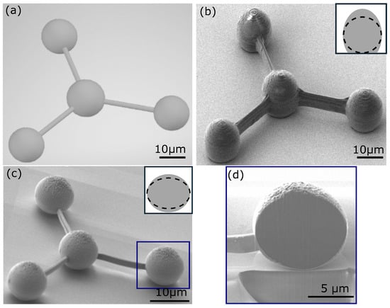
Figure 1.
(a) CAD model of a micro-optical system consisting of four interconnected micro-spheres, each with a diameter of 10 m. (b) SEM image of the microsystem fabricated with the dimensions of the CAD model using 2PP-lithography. The structure shows a clear distortion in the vertical direction. The section at the top right shows a schematic cross-section of one of the micro-spheres and the outer contour of the design geometry (dashed line). (c) SEM image of the microsystem produced with an adapted design geometry. The micro-spheres have a diameter of 10 m and a contact area of <1 to the substrate surface that was determined by SEM measurements and FIB cross-sections. The top right section shows a schematic cross-section of one of the micro-spheres and the outer contour of the design geometry (dashed line). (d) In the FIB cross-section, the shape fidelity and symmetry of the micro-sphere are evident.
To account for the observed deformations, the desired geometry must be adjusted based on the process parameters and voxel dimensions used in the 2PP-fabrication process, see Figure 2b. The geometry of the fabricated micro structure can be described by a convolution of the design geometry with the voxel geometry ,
Because of the large aspect ratio of the voxels, it is generally true that holds. This means the geometry applied during the fabrication process must be adapted, so that
The adapted geometry must be found by deconvolution. However, for the deconvolution to be a well posed problem in the sense of Hadamard, (i) must be a steady function and (ii) must have no roots.
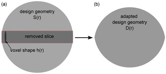
Figure 2.
Schematic illustration of an easy adaptation of the design geometry for the fabrication of a shape fidelity micro sphere. (a) Schematic cross-section of the design geometry for a micro sphere, the voxel geometry and the area to be removed in the center of the design geometry. (b) Resulting adapted geometry .
The implementation of the deconvolution process can be elaborate. However, a determination of the adapted geometry via a deconvolution is not necessary for the fabrication of fully symmetric structures such as micro spheres or biconvex lenses. Therefore, we can use a semi-empiric workflow as follows: (i) A design geometry is created and the voxel shape for the parameters used in the fabrication process is determined. (ii) A slice of the thickness of the voxel height is removed from the middle of the design geometry. (iii) The upper and lower sides of the design geometry are merged together, where the center of the adapted geometry match the center of the original design geometry.
Figure 2 shows a schematic visualization of these adaptations of the design geometry to the adapted geometry for fabrication. Thereby (a) shows the cross-section of the design geometry , the geometry of a voxel and the section to be removed in the center of the design geometry. (b) shows the adapted geometry for the manufacturing process. To create a micro sphere with a minimum contact area to the substrate, the center of the adapted geometry must remain at the position of the center point of the design geometry.
Achieving such precision requires detailed knowledge of the voxel dimensions so that the design can compensate for the inherent deformations introduced during fabrication. By incorporating this information into the design process, it is possible to anticipate 2PP-related deformations and generate a geometry tailored to the manufacturing parameters. This approach enables the fabrication of shape fidelity micro structures having any desired geometry. In addition, other process-related deviations, such as material shrinkage, can be addressed by adjusting the design geometry, further improving the fidelity of the fabricated structures. Figure 1c shows an SEM image of the microsystem shown in Figure 1a fabricated using an optimized design geometry. The micro-spheres retain the intended diameter of 10 m as shown in Figure 1b. However, there are slight surface imperfections, mainly due to residual polymer deposits that were not completely removed during the development process. For further validation, Figure 1d shows a cross-section of a full sphere cut by the FIB. Compared to the structure produced with the unadapted geometry, see Figure 1b, the optimized design shows a significant improvement in shape accuracy [].
These shape fidelity improvements enable the fabrication of micro-spheres using 2PP that match the geometric dimensions of commercially available micro-spheres. The high-resolution properties of conventionally fabricated micro-spheres are well described in the literature [,,]. The successful fabrication of 2PP micro-spheres with identical dimensions to their conventional counterparts allows us, for the first time, a direct comparison of their imaging properties. This provides a reliable demonstration of the high-resolution capabilities of micro structures fabricated using 2PP technology. To evaluate and compare imaging performance, micro-spheres with a diameter of 10 m were fabricated using 2PP. These micro-spheres were designed with a minimal contact area of less than 1 between the micro-sphere and the substrate, ensuring reduced optical interference from the substrate, as shown in Figure 1d. The diameter variations for the 2PP micro-spheres are in the range of the surface roughness of 10 nm and thereby one order of magnitude smaller than the diameter variations of the used PS micro-spheres from microparticels GmbH with ±100 nm. It should be noted that the diameter variations observed for the 2PP-fabricated micro-spheres are within the range of the measured surface roughness (approximately 10 nm). Such minimal dimensional deviations are negligible in comparison to the micro-spheres’ overall size and have no significant impact on their optical performance. After fabrication, the micro-spheres were carefully detached from the substrate and transferred to the sample for imaging experiments. For the high resolution imaging tests, a BluRay disc surface was chosen as the sample. The characteristic pits and lands on the disc surface provide a challenging test pattern for evaluating the resolution of optical systems.
3. Simulation of Imaging Properties
For a computational time optimized simulation of the imaging properties of the investigated optical biconvex micro structures, the Finite Refractive Index Selective Propagation (FRISP) method [] was extended by the optical properties of the microscope used for imaging. FRISP is based on scalar diffraction theory to determine the influence of a refractive micro structure on a wave field and provides a high correlation with the results of Finite Different Time Domain (FDTD) simulations and experiments for the determination of the focal properties of refractive micro structures [].
However, the simulation of the imaging properties of micro structures requires an extension of the FRISP method to include an object surface, the optical properties of the illumination and those of the microscope objective used for the high resolution imaging. In our case, the object surface is characterized by a binary amplitude mask . This simplified implementation allows us a rapid adaption of the object surface according to the test structure used in the experiments.
For the simulation of the illumination conditions used in the experiment, which satisfies all the characteristics of Köhler illumination, the illumination wavefront is divided into a series of plane waves with different angles of incidence.
where j is the description of the wave field with respect to the angle of incidence, is the wave vector and the complex amplitude at the position , with . The influence of the refractive micro structure on the wave field is determined for each of these illumination directions. For this purpose, the structure is divided into thin layers as described in [] and their influence on the wave field is determined. The propagation starts in the illumination plane at and stops in the object plane at . In the object plane, which is typically located directly below the refractive micro structure, the wave field is multiplied by the previously defined binary amplitude mask and the influence of the object on the wave field is taken into account by
representing the illumination wave field modeled with the object information and is used as the input wave field for the back propagation through the refractive micro structure.
In order to determine the imaging properties of the refractive micro structure, the wave field serves as the input wave field for the second propagation through the refractive micro structure. This wave field is again propagated through the micro structure using FRISP in the input plane of the illumination wave field. Finally, to obtain a focused image of the object surface, the wave fields are individually propagated into the image plane of the microscope objective for each illumination direction and the intensities are summarized incoherently by
which allows us to determine the intensity distribution of the high-resolution image recorded by the microscope in the experiment using a refractive micro structure on the surface of the object.
4. High Resolution Imaging: Results and Discussions
Figure 3 shows the experimental setup schematically and provides an SEM image of the surface structure of a BluRay disc. Imaging experiments were performed using a Zeiss AXIO Imager.A1m light microscope with a Zeiss microscope objective Epiplan-Neofluar HD 50x with a numerical aperture (NA) of 0.75. The illumination was provided by the halogen source built into the microscope and a passband filter with a central wavelength of 450 nm ± 10 nm. In particular, this microscope configuration makes it impossible to resolve the pits and lands of the BluRay disk without the aid of micro spheres, as the resolution limit according to the Rayleigh criterion [] for = 450 nm is 366 nm and the distance between the tracks of the BluRay is 320 nm.
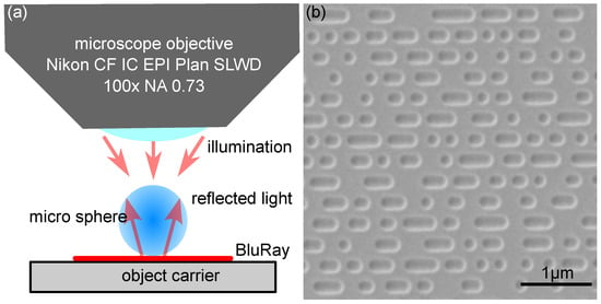
Figure 3.
(a) Schematic diagram of the experimental setup for high-resolution imaging using transparent micro-optical structures. The setup includes a light microscope equipped with a high numerical aperture objective, a halogen illumination source with a bandpass filter (centered at 450 nm), and a BluRay disc as the test sample. The micro-optical element is positioned on the sample surface, immersed in ethanol to facilitate manipulation and imaging. (b) SEM image of the BluRay disc surface, showing the characteristic pits and lands that serve as a challenging test pattern for evaluating the resolution capabilities of the fabricated micro-optics.
Figure 4 shows a side-by-side comparison of the imaging performance of conventional commercially available micro-spheres made and a micro-objective consiting of 4 micro-spheres fabricated by 2PP-lithography using IP-Dip (refractive index ) []. Both types of micro-spheres have a diameter of 10 m to ensure consistency in the comparison. In both cases, the fine surface features of the BluRay disc, including the individual horizontal tracks of the BluRay surface, with a track distance of 320 nm and the characteristic pits and lands, with lateral dimensions s small as 130 nm, are resolved, demonstrating the high-resolution imaging capabilities of these types of micro-spheres. The comparison highlights that 2PP micro-spheres can achieve imaging performance comparable to that of conventional commercially available micro-spheres. This result is significant as it confirms that 2PP lithography can fabricate optical micro structures suitable for high resolution imaging applications. Such verification via a comparison with conventional micro-spheres or reference literature has not been performed in previous publications [].
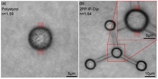
Figure 4.
Demonstration of the high-resolution properties for different materials with various refractive indices on the basis of micro-spheres with a diameter of 10 m. As test object the surface of a BluRay and as illumination a halogen lamp with a bandpass filter with a central wavelength of 450 nm ± 10 nm is used. Real high-resolution images of the test object with (a) commercially available polystyrene micro spheres (n = 1.59 []) and (b) micro-objectives made with 2PP using IP-Dip consisting of 4 micro spheres with connecting rods (n = 1.54 []) (see Figure 1). In all images, the fine surface features of the BluRay disc, including the individual vertical tracks of the BluRay surface and the characteristic pits and lands (see Figure 3b), are resolved. The red lines are guidelines for a better visualization of the direction and the distance of the BluRay tracks is 320 nm.
To demonstrate the potential of 2PP technology for the fabrication of refractive micro structures to be used in high-resolution microscopy, micro-objectives with biconvex micro lenses as central imaging element were fabricated using IP-Dip. The imaging properties of the biconvex micro lenses are compared with those of conventionally fabricated micro spheres and micro spheres fabricated using 2PP, as well as with simulation results based on the FRISP extension presented in Section 3.
Figure 5a shows an SEM image of a micro-objective, as introduced in Figure 1, with a biconvex micro lens with a radius of curvature of 12.5 m and an aperture diameter of 20 m as the central imaging element. The three micro spheres at the end of the connecting rods serve to stabilize the biconvex micro lens on the object surface and can be used for positioning on the object surface. The positioning of such a micro-objective can, for example, be done without contact using optical tweezers []. Figure 5b shows an optical microscope image with the experimental configuration shown in Figure 3. The central biconvex micro lens enables the resolution of the structures on the BluRay surface, with all surface details including the pit and lands structure. The zoom in of the area marked in (b) shown in (c) shows the clearly resolved pits and lands structure of the BluRay surface. This demonstration shows the usability of biconvex micro lenses for high-resolution imaging of structures below the diffraction limit and opens up new degrees of freedom for the design of the micro-optics used. By using the biconvex microlens as the central imaging optics, we were able to achieve the high resolution properties of the microspheres used in Figure 4 with a significant expansion of the field-of-view (FOV).
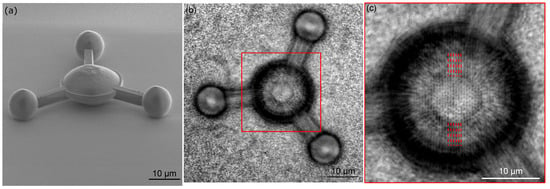
Figure 5.
Demonstration of the high-resolution properties of a biconvex micro lens. The test object is the surface of a BluRay and the illumination is provided by a halogen lamp with a bandpass filter with a central wavelength of 450 nm ± 10 nm. (a) SEM image of the micro-objective with a biconvex micro lens with a radius of curvature of 12.5 m, an aperture diameter of 20 m and an index of refraction of n = 1.54 [] as the central imaging element. (b) Light microscope image of the entire micro-objective, the marked area is shown enlarged in (c). In (b,c) the fine surface details of the BluRay disk, including the vertical tracks and the characteristic pits and lands of the BluRay surface are clearly resolved. The red lines in (c) serve as guidelines for a better visualization of the direction and distance of the BluRay tracks of 320 nm.
The previously mentioned extension of the FRISP method presented in Section 3 will be used to evaluate the additional degrees of freedom in the design opened up by the use of 2PP lithography for the fabrication of optical micro structures. In order to demonstrate the potential of this easily accessible simulation method, the experimental figures are compared with the predictions of the simulation in the following.
Figure 6 shows the comparison of the simulated intensity distributions of the central imaging element with the experimental images for the micro-objective made of micro spheres shown in Figure 4 and the biconvex micro lens shown in Figure 5a,b show the comparison of the intensity distributions for a micro sphere with a diameter of 10 m. The observed intensity peaks occurring at the edges of the micro sphere in the simulation in Figure 6a result from simulation artifacts. These artifacts are caused by the low amount of illumination directions, in this case 25, and the intense focusing of the micro sphere (photonic nanojet). Figure 5b,c shows the corresponding images for the micro lens with a radius of curvature of 12.5 m, an aperture diameter of 20 m. In this case, we can’t recognize the artefacts observed in (a), because the focus position is located in a wider distance from the object surface due to the smaller radius of curvature. The bright areas inside the high resolved area are the result of the higher contrast of the object surface during the simulation compared to the original BluRay in the experiment. The test object was a BluRay disk, which was also modeled in the simulation environment with its typical pits and lands structure. All four intensity distributions show clearly resolved traces in the vertical direction. Therefore, the simulation allows a reliable prediction of the imaging properties for different geometries of the central imaging elements of the investigated micro-objectives. In addition, the simulation also allows a prediction of the magnification through the micro-objective. In the simulation, the magnification is 1.63 for the micro spheres and 1.24 for the biconvex micro lenses. The magnification values match very well the values of 1.64 for the spheres and 1.21 for the biconvex lenses observed in the experiment. The deviation is mainly caused by slight shape deviation and differences in the refractive index between the parameters used in the simulation and the micro structures used in the experiment. Regarding the size of the FOV, there are slightly larger deviations between the simulation and the experimental observations. In addition to the above-mentioned deviation between the simulation and the experiment, the contrast between the pits and lands on the Blu-ray plays an important role in the valuation of the FOV. In the simulation, the contrast was assumed to be a step function with values of 0 and 1, which does not correspond to the contrast in the experiment. Because of the higher contrast in the simulation, the FOV seems larger than in the experiment.
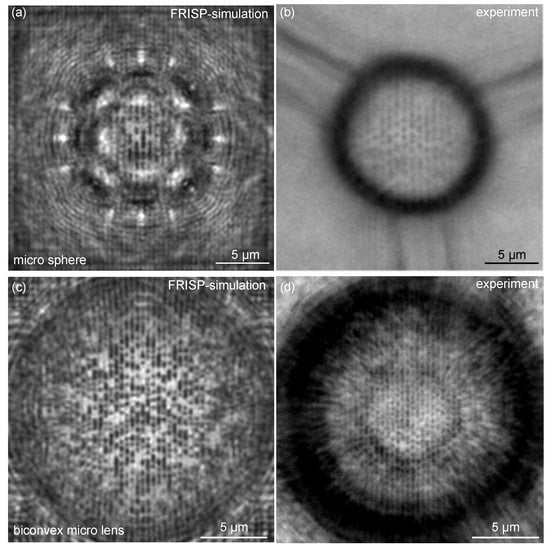
Figure 6.
Comparison of the imaging properties of the central imaging element of the micro-objectives in Figure 4 and Figure 5 with simulated intensity distributions. (a) Simulated intensity distribution in the image plane of a micro sphere with a diameter of 10 m and (b) the corresponding experimentally measured intensity distribution. the star-shaped bright areas in (a) are artifacts from the simulation. (c) Simulated intensity distribution in the image plane of the micro lens with a radius of curvature of 12.5 m, an aperture diameter of 20 m and (d) the corresponding experimentally measured intensity distribution.
To further demonstrate the versatility of 2PP-fabricated micro-optics for high-resolution imaging, future work will include imaging experiments in a broader range of samples, such as biological cells and nanostructured materials. This will further demonstrate the potential of the presented approach for applications in life sciences and nanotechnology.
5. Conclusions
In conclusion, we demonstrated the fabrication of shape-fidelity optical micro structures using 2PP for high resolution near-field microscopy. A challenge here are the small dimensions of the typically used optical micro structures with aperture and radii of curvature of less then 20 m. In order to demonstrate the potential of fabricating optical micro structures for this field of application, we compared the imaging properties with those of conventionally fabricated micro spheres. This comparison shows that micro structures fabricated using 2PP lithography are an alternative to the typically used micro spheres and open up additional degrees of freedom in the design of the used micro structures. To highlight these new degrees of freedom, for the first time we demonstrated imaging below the resolution limit using a biconvex micro lens in near-field microscopy.
The FRISP simulation method [] was extended to include the properties of the object illumination and the imaging properties of the microscope objective used for imaging, thus demonstrating a possibility for the computing time-optimized improvement of refractive micro structures for use in high-resolution near-field microscopy. The simulation enabled the prediction of the magnification caused by the optical micro structures on the object surface and thus the achievable resolution. Furthermore, the simulation gives a correct prediction of the position of the image plane relative to the object plane. Due to the accordance with the experimental data, FRISP is a valid alternative to the classically used FDTD simulations.
In addition, we demonstrated that the 2PP process allows a high degree of flexibility and additional degrees of freedom, enabling an individual adaptation of the dimensions and geometries of the micro structures. This adaptability was demonstrated by the fabrication of complex microsystems, such as the micro-objectives shown in Figure 1 and Figure 5. Furthermore, for the first time, an adapted geometry for high-resolution imaging using 2PP lithography was fabricated with a biconvex micro lens and proven to be applicable. This opens up new possibilities for the fabrication of complex microsystems with advanced optical designs tailored to specific high-resolution imaging applications.
Author Contributions
Conceptualization, F.T., M.A. and C.F.; methodology, F.T. and M.A.; software, F.T.; validation, F.T. and C.F.; formal analysis, F.T. and C.F.; investigation, F.T. and M.A.; resources, F.T.; data curation, F.T.; writing—original draft preparation, F.T. and M.A.; writing—review and editing, F.T., M.A., C.F. and R.B.B.; visualization, F.T. and M.A.; supervision, R.B.B. and C.F.; project administration, F.T.; funding acquisition, R.B.B. All authors have read and agreed to the published version of the manuscript.
Funding
The authors gratefully acknowledge the support of the Deutsche Forschungsgemeinschaft (DFG) for funding this work under the project “Hochauflösende optische Mikroskopie mittels transmissiver Mikrostrukturen—HOMiTrans”, grant no. 431605610.
Institutional Review Board Statement
Not applicable.
Informed Consent Statement
Not applicable.
Data Availability Statement
The raw data supporting the conclusions of this article will be made available by the authors on request.
Acknowledgments
The authors are grateful to Reiner Klattenhoff (BIAS) for his technical support with the optical setup and experimental work and Eva-Maria Meyer (IMSAS) for her support in the evaluation of the fabricated micro structures using SEM and FIB.
Conflicts of Interest
The authors declare no conflicts of interest.
References
- Abbe, E. Beiträge zur Theorie des Mikroskops und der mikroskopischen Wahrnehmung. Arch. Für Mikrosk. Anat. 1873, 9, 413–418. [Google Scholar] [CrossRef]
- Rayleigh, J.W.S. XXXI. Investigations in optics, with special reference to the spectroscope. Lond. Edinb. Dublin Philos. Mag. J. Sci. 1879, 8, 261–274. [Google Scholar] [CrossRef]
- Ash, E.; Nicholls, G. Super-resolution aperture scanning microscope. Nature 1972, 237, 510–512. [Google Scholar] [CrossRef]
- Hecht, B.; Sick, B.; Wild, U.P.; Deckert, V.; Zenobi, R.; Martin, O.J.; Pohl, D.W. Scanning near-field optical microscopy with aperture probes: Fundamentals and applications. J. Chem. Phys. 2000, 112, 7761–7774. [Google Scholar] [CrossRef]
- Hell, S.W. Far-field optical nanoscopy. Science 2007, 316, 1153–1158. [Google Scholar] [CrossRef]
- Rust, M.J.; Bates, M.; Zhuang, X. Sub-diffraction-limit imaging by stochastic optical reconstruction microscopy (STORM). Nat. Methods 2006, 3, 793–796. [Google Scholar] [CrossRef]
- Hell, S.W.; Wichmann, J. Breaking the diffraction resolution limit by stimulated emission: Stimulated-emission-depletion fluorescence microscopy. Opt. Lett. 1994, 19, 780–782. [Google Scholar] [CrossRef]
- Lee, J.Y.; Hong, B.H.; Kim, W.Y.; Min, S.K.; Kim, Y.; Jouravlev, M.V.; Bose, R.; Kim, K.S.; Hwang, I.C.; Kaufman, L.J.; et al. Near-field focusing and magnification through self-assembled nanoscale spherical lenses. Nature 2009, 460, 498–501. [Google Scholar] [CrossRef]
- Wang, Z.; Guo, W.; Li, L.; Luk’Yanchuk, B.; Khan, A.; Liu, Z.; Chen, Z.; Hong, M. Optical virtual imaging at 50 nm lateral resolution with a white-light nanoscope. Nat. Commun. 2011, 2, 218. [Google Scholar] [CrossRef]
- Zhu, H.; Chen, M.; Zhou, S.; Wu, L. Synthesis of high refractive index and shape controllable colloidal polymer microspheres for super-resolution imaging. Macromolecules 2017, 50, 660–665. [Google Scholar] [CrossRef]
- Kim, J.Y.; Pfeiffer, K.; Voigt, A.; Gruetzner, G.; Brugger, J. Directly fabricated multi-scale microlens arrays on a hydrophobic flat surface by a simple ink-jet printing technique. J. Mater. Chem. 2012, 22, 3053–3058. [Google Scholar] [CrossRef]
- Vlad, A.; Huynen, I.; Melinte, S. Wavelength-scale lens microscopy via thermal reshaping of colloidal particles. Nanotechnology 2012, 23, 285708. [Google Scholar] [CrossRef]
- Wang, H.; Shi, W.; Wang, J.; Zhou, X.; Li, P. Converting evanescent waves into propagating waves by hyper-hemi-microsphere. Opt. Express 2024, 32, 25451–25462. [Google Scholar] [CrossRef] [PubMed]
- Wu, G.; Zhou, Y.; Hong, M. Sub-50 nm optical imaging in ambient air with 10× objective lens enabled by hyper-hemi-microsphere. Light Sci. Appl. 2023, 12, 49. [Google Scholar] [CrossRef] [PubMed]
- Gissibl, T.; Thiele, S.; Herkommer, A.; Giessen, H. Sub-micrometre accurate free-form optics by three-dimensional printing on single-mode fibres. Nat. Commun. 2016, 7, 11763. [Google Scholar] [CrossRef]
- Marini, M.; Nardini, A.; Martínez Vázquez, R.; Conci, C.; Bouzin, M.; Collini, M.; Osellame, R.; Cerullo, G.; Kariman, B.; Farsari, M.; et al. Microlenses fabricated by two-photon laser polymerization for cell imaging with non-linear excitation microscopy. Adv. Funct. Mater. 2023, 33, 2213926. [Google Scholar] [CrossRef]
- Ren, H.; Jang, J.; Li, C.; Aigner, A.; Plidschun, M.; Kim, J.; Rho, J.; Schmidt, M.A.; Maier, S.A. An achromatic metafiber for focusing and imaging across the entire telecommunication range. Nat. Commun. 2022, 13, 4183. [Google Scholar] [CrossRef]
- Du, B.; Zhang, H.; Xia, J.; Wu, J.; Ding, H.; Tong, G. Super-resolution imaging with direct laser writing-printed microstructures. J. Phys. Chem. A 2020, 124, 7211–7216. [Google Scholar] [CrossRef]
- Thiemicke, F.; El-Bashar, R.; Hameed, M.F.; Agour, M.; Obayya, S.S.; Bergmann, R.B.; Falldorf, C. Fast simulation of the influence of a refractive free-form microstructure on a wave field based on scalar diffraction theory. J. Eur. Opt. Soc.-Rapid Publ. 2025, 21, 4. [Google Scholar] [CrossRef]
- Thiemicke, F.; Falldorf, C.; Bergmann, R.B. Fabrication of positionable free-standing microstructures for applications in near-field microscopy. DGaO Proceedings 2024, 10744, B013–B014. Available online: http://www.dgao-Proceedings.de (accessed on 2 July 2025).
- Wang, H.; Zhang, W.; Ladika, D.; Yu, H.; Gailevičius, D.; Wang, H.; Pan, C.F.; Nair, P.N.S.; Ke, Y.; Mori, T.; et al. Two-photon polymerization lithography for optics and photonics: Fundamentals, materials, technologies, and applications. Adv. Funct. Mater. 2023, 33, 2214211. [Google Scholar] [CrossRef]
- Villangca, M.J.; Palima, D.; Banas, A.R.; Glückstad, J. Light-driven micro-tool equipped with a syringe function. Light Sci. Appl. 2016, 5, e16148. [Google Scholar] [CrossRef] [PubMed]
- Huszka, G.; Yang, H.; Gijs, M.A. Microsphere-based super-resolution scanning optical microscope. Opt. Express 2017, 25, 15079–15092. [Google Scholar] [CrossRef]
- Jiang, W.; Wang, J.; Yang, Y.; Bu, Y. A Review of Microsphere Super-Resolution Imaging Techniques. Sensors 2024, 24, 2511. [Google Scholar] [CrossRef]
- Dottermusch, S.; Busko, D.; Langenhorst, M.; Paetzold, U.W.; Richards, B.S. Exposure-dependent refractive index of Nanoscribe IP-Dip photoresist layers. Opt. Lett. 2018, 44, 29–32. [Google Scholar] [CrossRef]
- Sultanova, N.; Kasarova, S.; Nikolov, I. Dispersion properties of optical polymers. Acta Phys. Pol. A 2009, 116, 585–587. [Google Scholar] [CrossRef]
Disclaimer/Publisher’s Note: The statements, opinions and data contained in all publications are solely those of the individual author(s) and contributor(s) and not of MDPI and/or the editor(s). MDPI and/or the editor(s) disclaim responsibility for any injury to people or property resulting from any ideas, methods, instructions or products referred to in the content. |
© 2025 by the authors. Licensee MDPI, Basel, Switzerland. This article is an open access article distributed under the terms and conditions of the Creative Commons Attribution (CC BY) license (https://creativecommons.org/licenses/by/4.0/).