Article

High-Efficiency, Low-Power, Fully Integrated Neural Electrical Stimulation Circuit

1
School of Microelectronics, Shanghai University, Shanghai 201800, China
2
MTRIX Corporation, Shanghai 201800, China
*
Author to whom correspondence should be addressed.
Appl. Sci. 2025, 15(12), 6737; https://doi.org/10.3390/app15126737
Submission received: 27 May 2025 / Revised: 11 June 2025 / Accepted: 11 June 2025 / Published: 16 June 2025
(This article belongs to the Special Issue Low-Power Integrated Circuit Design and Application)

Abstract

:
This paper presents a highly efficient, low-power, fully integrated neural stimulation circuit implemented using solely low-voltage devices. The circuit primarily consists of a high-voltage-generation circuit, an output driver circuit, and a constant-current source, designed and simulated using a 180 nm low-voltage CMOS process. The high-voltage-generation circuit utilizes a negative-voltage-generation module together with a series–parallel capacitor charge pump circuit, which effectively reduces the number of charge pump stages by three, and saves 29% of the area compared to a conventional charge pump circuit. A bootstrap clock generation circuit was utilized to generate the control signal to ensure that all transistors work within their voltage limit. To realize the high-voltage output driver circuit using low-voltage devices, a stacked transistor structure with deep N-well (DNW) devices was utilized. The four different output voltage levels from the high-voltage-generation circuit were utilized to generate a different voltage domain of control signals and bias voltage for the stacked transistors, making sure that all transistors work within their voltage limit. Simulation results show that the high-voltage-generation circuit can generate an output of up to 12.69 V from a 1.65 V low input voltage, with a maximum output current of 1 mA, achieving 74.9% efficiency. The overall efficiency of the neural stimulation circuit, including the high-voltage-generation circuit, output driver circuit and constant-current source, reaches 74% under the voltage-controlled stimulation (VCS) mode and 59.5% under the current-controlled stimulation (CCS) mode, whereas the standby static power consumption is as low as 66 pW.

1. Introduction

At present, there are more and more patients with brain diseases, and traditional drug treatment can no longer meet the demand, so the research in the field of the brain and brain diseases has become a hot research direction. Brain–computer interface technology (BCI) is an advanced brain science research technology. By implanting electrodes at designated positions, the brain can transmit information to external devices, so as to stimulate nerves. Neural stimulation is an important part of a brain–computer interface. It injects a specific amount of charge into nerve tissue through electrodes and produces a certain physiological response, so as to achieve the purpose of treatment [1]. Neural stimulation technology has been widely used in cochlear implantation, neuromuscular stimulation and deep-brain stimulation [2,3,4]. It not only realizes the modulation and decoding of neural signals but also provides users with more accurate and efficient human–computer interaction through function recovery, behavior intervention and neural feedback. At present, there are three main types of neural stimulation circuits: voltage-controlled, current-controlled and charge-controlled stimulation. Voltage-controlled stimulation is the earliest nerve stimulation mode applied in history [5]. It achieves the purpose of stimulation by applying a fixed voltage at both ends of the electrodes. Although this mode has the benefit of low power consumption, the stimulation current is uncontrollable, which is prone to cause irreversible damage to the tissue. On the other hand, charge-controlled stimulation injects the charge into the target tissue [6]. It is safer, but it needs to be realized using bulky capacitors, which limits the miniaturization of the neural stimulation circuit. Current-controlled stimulation is the most used stimulation method at present, as the stimulation current is controllable, which is therefore a safer option.
When applying neural stimulation, the electrode–tissue interface generally requires a stimulation current as high as 1 mA [7]. Utilizing a well-designed electrode, the electrode–tissue impedance can be in the range of a few tens of kilo-Ohms to mega-Ohms [8]. Therefore, it would require the stimulation circuit to sustain more than 10 V voltage, making high-voltage generation an essential part of a current-controlled stimulation circuit. To achieve high efficiency remains a critical challenge for the design of the high-voltage-generation circuit.
In 2012, Arfine et al. proposed a high-voltage-generation circuit that monitors and regulates the DC-DC converter current [9] using a current sensor, thus reducing energy waste. However, this method utilizes large inductance. In 2013, H. Lee proposed a head-mounted deep-brain stimulator [10], which regulates the supply voltage and improves the efficiency, but this method increases the complexity of the circuit. In 2017, Z. Luo et al. proposed a neurostimulation [11], which combined digitally adjusting the supply voltage, achieving an efficiency of 54%. However, the supply voltage of each channel cannot be individually controlled. In 2024, Peking University proposed a high-energy-efficiency current-mode neurostimulator [12] based on the dynamic power supply voltage. It can achieve a significant increase in the efficiency of the system. However, this method also utilizes a large inductor.
In this paper, we propose a neural stimulation circuit designed solely using low-voltage devices under the standard CMOS process. It eliminates the usage of bulky high-voltage devices and reduces the fabrication cost. More importantly, it allows a more compact integration with the recording and signal processing circuit using the standard CMOS process to form a complete closed-loop brain–computer interface system. A series–parallel charge pump with a negative-voltage assist module was utilized to generate high-voltage output, which reduces the number of charge pump stages at the same time to improve the efficiency of the circuit. The output driver circuit utilizes the different voltage levels output from the high-generation circuit to control and bias the stacked transistors, ensuring the devices do not exceed their voltage limit.
The structure of this paper is as follows: Section 2 introduces the system architecture, Section 3 describes the circuit design, Section 4 presents the simulation results and Section 5 provides the conclusion.

2. Overall Neural Stimulator System

Figure 1 shows the overall system architecture of the neuroelectric stimulator, which consists of three main modules: the high-voltage-generation circuit, the output driver circuit and the constant-current source. The high-voltage-generation circuit provides four stable step-up voltage levels from Vout1 to - Vout4 to the output driver circuit of the neurostimulator. The output driver circuit delivers the necessary stimulation current to the electrodes of the nerve tissues. The constant-current source provides an adjustable and constant current to the neural stimulator.

3. Circuit Design

3.1. High-Voltage-Generation Circuit Design

Typically, there are two methods to realize high-voltage-generation circuits: DC-DC converters and charge pump circuits. DC-DC converters mainly consist of capacitors, inductors, diodes and transistors. However, for implantable chips, inductive components are generally bulky and impose risks for electromagnetic compatibility, making capacitor-based energy storage charge pumps the only viable option for on-chip high-voltage-generation circuits. The CW charge pump, as the earliest charge pump scheme (proposed in 1932), has the structure shown in Figure 2a [13]. However, the biggest problem of this scheme is that it is highly sensitive to parasitic capacitance. Subsequently, Dickson proposed a new charge pump design scheme, which is based on a diode and pump capacitor composition. The structure is shown in Figure 2b. The circuit uses a number of diodes to prevent current backflow [14,15]. With excellent performance, this design is widely adopted in mainstream high-voltage-generation circuits. However, this scheme still suffers from limitations, such as fixed gain and a large device area. Therefore, it is not suitable for systems with small area requirements.
Although conventional charge pumps are easy to implement, their efficiency is relatively low due to the threshold voltage drop of diodes. To address this limitation, the conventional series–parallel charge pump replaces the diodes with CMOS switches, as shown in Figure 3. When the clock is high, all capacitors are charged by Vin, and the voltage difference between the upper and lower plates of the capacitors is 1.65 V. When the clock is low, the capacitors are connected in series, resulting in high-voltage output.
This paper presents a proposed series–parallel charge pump structure with a negative-voltage-generation module, as shown in Figure 4. Compared to conventional charge pump circuits, this architecture is capable of generating high voltages using a low-voltage CMOS process and reduces the number of stages required to achieve the same voltage conversion rate, thereby reducing the number of capacitors required and achieving a small area. Moreover, it enables the system to have a standby static power consumption as low as the picowatt level and to maintain high efficiency over a wide range of output currents. To achieve an output voltage above 12 V, the proposed series–parallel structure needs only four stages (N = (Vout − Vin)/3.3 V), in which 3.3 V is the voltage difference between the two plates of the capacitor in the charging stage, whereas conventional series–parallel structure needs seven stages due to lower voltage (1.65 V) stored on the capacitors. By saving three charge pump stages, the proposed charge pump saves 29% area compared to conventional structure, at the same time improving the power efficiency.
The power consumption of the charge pump mainly comes from the dynamic power consumption of the switches. The larger the number of switches, the higher the dynamic power consumption. Similarly, high switching frequency leads to greater switching losses and reduced efficiency. However, high-frequency switching reduces the ripple of the output voltage. Hence, there is a trade-off to consider when deciding on the switching frequency. Besides switching losses, the efficiency of the charge pump is also affected by the on-state voltage drop of the switching devices. The increase in the number of stages may improve the voltage conversion efficiency, but each stage introduces additional losses.
The negative-voltage-generation module of the high-voltage-generation circuits is shown in Figure 5a, and the series–parallel charge pump circuit is shown in Figure 5b. The operation of the negative-voltage-generation circuit can be divided into two states: capacitor charging state (shown by the red dashed line in Figure 5a) and voltage generation state (shown by the blue dashed line in Figure 5a). When CLK is low, the negative-voltage module charges capacitor C0, Mp1 and Mn3 conduct, and Mn1 and Mn2 are disconnected. During this period, the C0− end of the capacitor is connected to the input voltage of 1.65 V, the C0+ end is connected to GND, and the voltage difference between the upper and lower plates of capacitor C0 is 1.65 V. VDD/2 is chosen as the input charging voltage to make sure that the voltage stored on the capacitors is within VDD, and this VDD/2 voltage is provided by the voltage generation circuit of the stimulation system. When CLK is high, Mn1 and Mn2 conduct, and Mp1 and Mn3 are disconnected. During this period, C0− is connected to GND. Since the voltage at both ends of the capacitor does not change abruptly, the voltage at C0+ is pulled down to −1.65 V. In order to prevent the parasitic diode in Mn2 from turning on when the voltage at C0+ is −1.65 V, Mn2 adopts a deep N-well (DNW) device. In addition, considering that vp is a negative voltage and CLKB is a low voltage, Mn3 generates leakage current. A diode Mp6 is added between C0+ and Mn3 to prevent leakage current in Mn3.
The series–parallel charge pump operates in two phases: charging and discharging. When CLK is high, the capacitor is charged, and its path is shown by the blue dotted line in Figure 5b. Mn4–Mn11 are on, Mp2–Mp5 are off, and the negative-voltage outputs are connected to Mn4, Mn6, MN8 and Mn10. Take capacitor C1 as an example. At this time, C1− is connected to −1.65 V, C1+ is connected to 1.65 V, capacitor C1 is charged, and the capacitor voltage difference between the upper and lower plates is 3.3 V. When CLK is low, the capacitor series discharge, as shown by the red dotted line in Figure 5b. During this period, Mn4–Mn11 are disconnected, and Mp2–Mp5 are on. Taking capacitor C1 as an example, the voltage at the C1− end is 1.65 V. Since the voltage at both ends of the capacitor does not change abruptly, the voltage at the C1+ end becomes 4.95 V (1.65 + 3.3 V), i.e., Vout1 = 4.95 V. Similarly, Vout2 = 8.25 V (4.95 V + 3.30 V), Vout3 = 11.55 V (8.25 V + 3.30 V) and Vout4 = 14.85 V (8.25 V + 3.30 V).
The capacitor size was determined based on the maximum stimulation current and the maximum stimulation pulse width of the stimulator. With a stimulation current of 1 mA and pulse width of 1 ms, the stimulation charge would be Qload = 1 μC, calculated by Q = I × T. Assuming that the load consumes 40% of the charge stored on the capacitors, the total charge of the series–parallel charge pump system would be Qtotal = 2.5 μC, which is also equal to the charge stored on a single capacitor Qsingle = 2.5 μC. From Q = C × V, we get the value of the single-stage capacitor Csingle = 0.76 μF when V = 3.3 V. For the negative-voltage module, assuming the charge transfer efficiency is at 40%, then the negative-voltage module needs to store a charge of Qneg_total = 6.25 μC. According to the charging voltage difference of its storage capacitance of 1.65 V and C = Q/V, the capacitance value required is Cneg = 3.8 μF. This calculation is universal, and the load charge can be recalculated when the stimulus current or the pulse width is changed, and the capacitance value of the various levels of storage capacitance can be solved.
A bootstrap circuit, as shown in Figure 6, is used to control the gate of transistor Mn2 to make sure the gate-source voltage difference of Mn2 does not exceed the device limit. If an ordinary clock signal is used to control switch Mn2, when the vp terminal is connected to GND, the clock signal is at a low level, and the circuit is shut down normally. When the vp terminal generates a negative voltage −1.65 V, the clock is at a high level, the voltage difference between the source and gate of the NMOS is 4.95 V, which exceeds the transistor’s voltage limit.
The timing diagram of the bootstrap circuit is shown in Figure 7. It is important to ensure that Mn13 and Mp7 do not turn on at the same time.
When CLK is low, the capacitor is charged, and vp is connected to GND. During this period, Mp7 and Mn13 conduct, Mn12 is off, and Vm is connected to VDD. At this time, the gate control signal V0 of the negative-voltage circuit transistor Mn2 potential is connected to GND, turning off Mn2. Conversely, when CLK is high, the vp voltage is pulled down to −1.65 V. As the capacitor voltage does not change abruptly, Vm is pulled to 1.65 V. Transistors Mp7 and Mn13 are off, and Mn12 is on. At this time, V0 voltage is at 1.65 V, and the gate-source voltage of Mn2 is 3.3 V, within the voltage limit of the device.

3.2. Constant-Current Source Design

Current-controlled stimulation (CCS) is by far the most commonly used stimulation mode. In this mode, the circuit requires a constant-current source to provide the stimulation current. The structure of the constant-current source is shown in Figure 8. It mainly consists of a bandgap reference circuit (as in Figure 9) and a current DAC (as in Figure 10).
The bandgap reference circuit adds the positive- and negative-temperature coefficient currents to obtain a temperature-independent reference current. The reference source circuit consists of two parts: the start-up circuit and the core circuit.
The designed start-up circuit operates as follows: when the circuit is first started, the gate voltage of M10 is close to 0. With the increase in VDD, the source voltage of M10 increases, the transistor conducts, and the drain voltage of M10 increases, until the circuit enters into normal operation. When the circuit works normally, the drain potential of M12 and M17 decreases, making M1 conductive, pulling up the gate voltage of M10. M10 turns off, which in turn turns off the startup circuit, and the bandgap reference circuit enters the normal operating state.
The core circuit consists of MOS tubes M11–M14 and M17; BJT tubes M15 and M16; and resistors R1, R2 and R3. M15 and M16 are PNP-type transistors, and the emitter area ratios of M15 and M16 are set at 1:n. Assuming that the ratio of M15 to M16 is 1:n, the expression for the output current is shown in Equation (1):
I r e f = V B E 15 R 1 + V T ln n R 2
The current DAC configures the output current via C<5:0> and CT<2:0>. In order to reduce the mismatch of devices, the current DAC uses low 6-bit binary code and high 3-bit thermometer code.
The core of the circuit consists of two parts: one is the weighted current array, which uses a binary weighted current source M28–M36 and binary weighted control switches. The current is determined by setting the MOS tube aspect ratio of the current source, and the aspect ratio is scaled by a ratio of 2n to ensure the accuracy of current matching. The switching signals C<5:0> and CT<2:0> are set to be active low. The current resolution of the DAC is 4 μA:
I D A C , M A X = I r e f n = 0 5 2 n C < n > ¯ + m = 0 2 2 6 C T < m > ¯

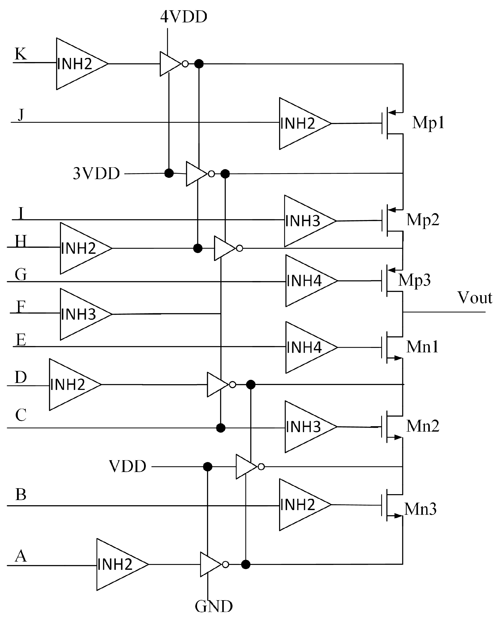
3.3. Output Driver Circuit Design

The output driver circuit is implemented solely using low-voltage devices, as shown in Figure 11.
Three 3.3 V DNW NMOS devices and three 3.3 V PMOS devices are stacked to withstand a 12.6 V supply voltage. The control signals A–K are set to GND, VDD, 2 VDD, 2 VDD, 3 VDD, 3 VDD, 3 VDD, 3 VDD, 3 VDD, 3 VDD and 3 VDD. At this time, Mp1–Mp3 is on, Mn1–Mn3 is off, and the output voltage Vout = 4 VDD. By further setting the values of different control signals, the circuit can realize the dynamic switching of the output voltage, and can switch Vout from GND to 4 VDD, and then from 4 VDD to GND.

4. Results

The layout of the system was designed based on the SMIC 180 nm process, as shown in Figure 12. The core area is 341 μm × 226 μm.

4.1. High-Voltage-Generation Circuit Simulation

Post-layout simulation was performed for the high-voltage-generation circuit. The CLK frequency of the high-voltage-generation circuit is 500 Hz. The output waveform with no-load is shown in Figure 13, whereas Figure 14 shows the output waveform when the load current is 1 mA. Under the no-load condition, the circuit converts the input voltage of 1.65 V into the output voltages of 4.20, 7.02, 9.86 and 12.69 V.
The ripple of the output voltage after stabilization is lower than 0.244% (as shown in Figure 15). The proposed circuit supports four output voltages, up to 12.69 V with a maximum 1 mA load current. The efficiency of the circuit can be calculated from Equation (3).
η = P o u t P i n
The maximum efficiency of 74.9% is achieved when the output current is 1 mA; the output voltage is 12.69 V, at which the input voltage is 1.65 V; and the input current is 5.76 mA. It is particularly noteworthy that it has the characteristics of an ultra-low-voltage ripple, which is an important parameter for the application of nerve stimulation. An excessive ripple may lead to current fluctuation and affect the effect of stimulation.
Figure 16, shows the efficiency of the high-voltage-generation circuit with different load conditions. At a light load, fixed losses dominate (capacitive dielectric time losses, parasitic capacitance charging and discharging losses, switching device turn-off losses), thus reducing efficiency. As the load increases, the variable losses (losses in switching device on-resistance, heat from capacitor charging and discharging, switching losses) are quadratically related to the current, which results in the efficiency decaying beyond the optimum point.
Meanwhile, in order to evaluate the influence of the variation of the manufacturing process parameters on the circuit performance, we simulated the charge pump circuit over different process corners, and the simulation results are shown in Figure 17. It can be seen that the output voltage with no load is above 12.4 V over different process corners. The transistors have been sized to make sure that they operate under the desired operating region over different process corners.
Table 1 summarizes the performance of the proposed high-voltage-generation circuit and compares it to the previously published charge pump IC that provides output voltages in excess of 10 V and a wide range of current loads. The circuit supports four output voltages, with high voltages up to 12.69 V, a maximum load current of 1 mA and an efficiency of 74.9%. The proposed circuit achieves an ultra-low-voltage ripple, an important criterion for neurostimulation applications. An excessive ripple may cause current fluctuation and affect the effect of stimulation. While the design in reference [8] achieves comparable output voltages, it has low efficiency and low load current. On the other hand, ref. [16] achieved a relatively high efficiency of 84.7% using a 0.18 μm CMOS process. However, it has a lower voltage conversion ratio compared to our design and a relatively high-voltage ripple of 1% at maximum load. Reference [17] achieves lower voltage generation capability but lower peak efficiency. Reference [18] uses a dedicated 0.18 μm CMOS high-voltage process to achieve a 20 V output. This high-voltage approach can simplify some aspects of high-voltage power generation but typically has high complexity and cost.
This good power efficiency indicates that our charge pump can convert input power to output power with minimal energy loss over a wide range of load currents. As shown in Table 1, our charge pump achieves a good balance between voltage output, load current support, voltage ripple and power efficiency compared to other designs.

4.2. Constant-Current Source Simulation

The module is simulated with a temperature scan from −40 °C to 125 °C, and the current output results are shown in Figure 18.
The calculation of the temperature coefficient is shown in Equation (4):
T C = I m a x I m i n I r e f × Δ T × 10 6
The temperature coefficient achieved by the bandgap reference current circuit is 49.3 ppm/°C from −40°C to 125°C.
The current DAC is controlled by a 9-bit binary control code. The circuit simulation shows that the output current can be varied in the range of 0–1 mA. Under the condition of minimum range (digital code 111111111), the actual output current of the circuit is 4 μA, which matches the theoretical value. Under the condition of full-scale output (digital code 000000000), the measured current is 944.8 μA (the theoretical value is 1 mA), and the error with the theoretical value is only 5.52%

4.3. Output Driver Circuit Simulation

The waveform of the output voltage is shown in Figure 19 under no-load conditions. It shows that when the control signal is triggered according to the preset logic timing, the PMOS/NMOS switches of the driver circuit can accurately switch to the cascade path of the charge pump, so that the output voltage reaches the maximum value of 12.60 V. It is worth noting that the timing control of the driver circuit introduces a delay of 2.7 ns, which mainly originates from the charging and discharging process of the switching tubes. By optimizing the size of the driver transistors, the delay can be controlled within the system allowable range, ensuring the synchronization of the high-voltage signal with the stimulus pulse.

4.4. Neural Stimulation System

The static current of the entire neural stimulation system in standby mode is shown in Figure 20. According to P = I × V, we can calculate the static power consumption in standby to be 66 pW.
The proposed circuit was simulated under the voltage-controlled stimulation (VCS) mode with an external 150 kΩ load resistor, as shown in Figure 21. The simulated results are shown in Figure 22, where VDD4 is the output voltage of each stage of the charge pump, and VOUT1 is the output voltage of the output stage. When the system performs single-phase stimulation, the voltage difference between the output of the stimulator and the charge pump output is 0.15 V, and the efficiency of the circuit is 74%.
The current-controlled stimulation mode allows for more precise neural stimulation through constant-current output, and the circuit connections are shown in Figure 23.
The simulation result when the resistance is 10 kΩ and the DAC output current is 945 μA (digital control code is 000000000) is shown in Figure 24, where VOUT1 is the output voltage of the output driver, VOUT2 is the voltage across the current source, and VOUT1–VOUT2 is the voltage drop across the load resistor.
In order to simulate the scenario in real application, we connected a 30 kΩ resistor and a 50 nF capacitor in series between the channels, and the connection is shown in Figure 25. According to the actual application requirements, the control parameters of the DAC were set to configure the stimulation current as 252 μA and the stimulation time as 1 ms. The output waveforms are shown in Figure 26 (VOUT1 is the output voltage of the output driver; VOUT2 is the output voltage of the current source).
The stimulation efficiency at different output currents can be calculated according to Equation (5) of the efficiency calculation. The relationship between efficiency and the current is shown in Figure 27. It can be seen that the maximum efficiency of the circuit can reach 59.5%.
η = P o u t P i n
Table 2 shows the performance summary of the proposed neural stimulation system compared to prior articles. Under the CCS stimulation mode, the efficiency of the proposed circuit in this paper is higher compared to other structures and has lower standby power consumption.

5. Conclusions

This paper presents a low-power, high-efficiency, high-voltage (12.69 V) neural electrical stimulation circuit implemented solely using low-voltage devices under the standard CMOS process. A negative-voltage-based series–parallel charge pump was proposed to generate high voltage for the stimulation system. Compared to conventional charge pumps, this structure achieves higher voltage gain with fewer stages and a smaller area while maintaining high power efficiency. Additionally, compared to other high-voltage-generation circuit structures used in neural stimulation circuits, it exhibits a lower output voltage ripple. A stacked transistors structure was used to implement the output driver circuit. Utilizing the different output voltage levels from the high-voltage-generation circuit, the devices of the output driver circuit were ensured to operate within their voltage limit. Simulation results show that at a maximum current load of 1 mA, the efficiency of the high-voltage-generation circuit is 74.9%, and the output voltage ripple is 0.244%. The output voltages are 4.20, 7.02, 9.86 and 12.69 V. The standby power consumption of the entire simulated system is 66 pW. High-voltage output functionality can be achieved through the output driver. The maximum efficiency of the entire system is 59.5%.
The designed neurostimulation circuit can be used in practical applications to form a completed brain–computer interface system by working with multiple systems, such as wireless charging circuits. Implanted in the brain, the circuit can be used to inhibit neurological disorders such as epilepsy by injecting a specified amount of electrical charge into the neural tissue to stimulate a physiological response.

Author Contributions

Conceptualization, Y.W.; Methodology, Y.W.; Software, Y.W.; Validation, Y.W.; Formal analysis, Y.W.; Investigation, Y.W.; Resources, Y.W.; Data curation, Y.W.; Writing—original draft, Y.W.; Writing—review & editing, Y.W. and J.C.; Visualization, Y.W.; Supervision, J.C.; Project administration, C.L.; Funding acquisition, C.L. All authors have read and agreed to the published version of the manuscript.

Funding

This research is supported by Lingang Laboratory Key Project LG-GG-202402-05-02.

Institutional Review Board Statement

Not applicable.

Informed Consent Statement

Not applicable.

Data Availability Statement

The original contributions presented in the study are included in the article, further inquiries can be directed to the corresponding author.

Conflicts of Interest

Author Jiahao Cheong was employed by the company MTRIX Corporation. The remaining authors declare that the research was conducted in the absence of any commercial or financial relationships that could be construed as a potential conflict of interest.

References

  1. Chen, W.M.; Chiueh, H.; Chen, T.J. A fully integrated 8-channel closed-loop neural-prosthetic SoC for real-time epileptic seizure control. In Proceedings of the IEEE International Solid-State Circuits Conference Digest of Technical Papers, San Francisco, CA, USA, 17–21 February 2013; Volume 49, pp. 286–287. [Google Scholar]
  2. Oluigbo, C.O.; Salma, A.; Rezai, A.R. Deep Brain Stimulation for Neurological Disorders. IEEE Rev. Biomed. Eng. 2012, 5, 88–99. [Google Scholar] [CrossRef] [PubMed]
  3. Lu, Z.; Chen, W.; Liu, X. A High-voltage Tolerant and Current-accurate Neural Stimulator Based on A Low-voltage CMOS Process. In Proceedings of the IEEE Asia Pacific Conference on Circuits and Systems (APCCAS), Taipei, Taiwan, 7–9 November 2024; pp. 562–565. [Google Scholar]
  4. Ahn, W.; Kim, D.; Park, J. A Reconfigurable Neural Stimulation IC with a High-Resolution Strength Control and In-Situ Neural Recording Function for Cochlear Implant Systems. IEEE Solid-State Circuits Lett. 2022, 5, 162–165. [Google Scholar] [CrossRef]
  5. Huang, Y.E.; Peng, S.Y. A Current-Mode Electrical Stimulator with Charge Balance for Neural Stimulation Applications. In Proceedings of the IEEE Asia Pacific Conference on Circuits and Systems (APCCAS), Taipei, Taiwan, 7–9 November 2024; pp. 772–775. [Google Scholar]
  6. Xin, H.; Zhou, M.; Wegberg, R.V. A 16-Output 10-V Compliant Stimulator ASIC with Sub-10-nA Mismatch and Simultaneous ETI Sensing for Selective Neural Stimulation. IEEE J. Solid-State Circuits 2025, 60, 908–920. [Google Scholar] [CrossRef]
  7. Alfia, A.; Hyouk-Kyu, C. A regulated multiple-output high-voltage charge pump IC for implantable neural stimulators. Microelectron. J. 2019, 92, 104617. [Google Scholar] [CrossRef]
  8. Bisoni, L.; Carboni, C.; Raffo, L.; Carta, N.; Barbaro, M. An HV-CMOS Integrated Circuit for Neural Stimulation in Prosthetic Applications. IEEE Trans. Circuits Syst. II Express Briefs 2015, 62, 184–188. [Google Scholar] [CrossRef]
  9. Arfin, S.K.; Sarpeshkar, R. An Energy-Efficient, Adiabatic Electrode Stimulator with Inductive Energy Recycling and Feedback Current Regulation. IEEE Trans. Biomed. Circuits Syst. 2012, 2, 1–14. [Google Scholar] [CrossRef] [PubMed]
  10. Lee, H.M.; Park, H.; Ghovanloo, M. A Power-Efficient Wireless System with Adaptive Supply Control for Deep Brain Stimulation. IEEE J. Solid-State Circuits 2013, 48, 2203–2216. [Google Scholar] [CrossRef] [PubMed]
  11. Luo, Z.; Ker, M.D.; Yang, T.Y.; Cheng, W.H. A Digitally Dynamic Power Supply Technique for 16-Channel 12 V-Tolerant Stimulator Realized in a 0.18- μm 1.8-V/3.3-V Low-Voltage CMOS Process. IEEE Trans. Biomed. Circuits Syst. 2017, 11, 1087–1096. [Google Scholar] [CrossRef] [PubMed]
  12. You, Y.; Tian, R.; Zhang, Y.; Chen, Z.; Lu, W.; Zhang, Y. A High-Voltage-Compliant 86% Peak Efficiency Current-Mode Stimulator with Dynamic Voltage Supply for Implantable Medical Devices. IEEE J. Solid-State Circuits 2024, 35, 1–13. [Google Scholar] [CrossRef]
  13. Tanzawa, T. On-Chip-High-Voltage Generator Design: Design Methodology for Charge Pumps, 2nd ed.; Springer International Publishing: Berlin/Heidelberg, Germany, 2016; ISBN 978-3-319-21974-5. [Google Scholar]
  14. Ballo, A.; Grasso, A.D.; Palumbo, D. A Bulk Current Regulation Technique for Dual-Branch Cross-Coupled Charge Pumps. IEEE Trans. Circuits Syst. II: Express Briefs 2022, 69, 4128–4132. [Google Scholar] [CrossRef]
  15. Ballo, A.; Grasso, A.D.; Palumbo, G. A Review of Charge Pump Topologies for the Power Management of IoT Nodes. Electronics 2019, 8, 480. [Google Scholar] [CrossRef]
  16. Abdi, A.; Kim, H.S.; Cha, H.K. A High-Voltage Generation Charge-Pump IC Using Input Voltage Modulated Regulation for Neural Implant Devices. IEEE Trans. Circuits Syst. II Express Briefs 2019, 66, 342–346. [Google Scholar] [CrossRef]
  17. Zhou, Y.; Wang, K.; Yin, S. A Fully Integrated Stimulator with High Stimulation Voltage Compliance Using Dynamic Bulk Biasing Technique in a Bulk CMOS Technology. IEEE Trans. Circuits Syst. I Regul. Pap. 2024, 71, 2525–2537. [Google Scholar] [CrossRef]
  18. Zhao, J.; Yao, L.; Xue, R.F.; Li, P.; Je, M.; Xu, Y.P. An Integrated Wireless Power Management and Data Telemetry IC for High-Compliance-Voltage Electrical Stimulation Applications. IEEE Trans. Biomed. Circuits Syst. 2016, 10, 113–124. [Google Scholar] [CrossRef] [PubMed]
  19. Urso, A.V.; Giagka, M.; Dongen, V.; Serdijn, W.A. An Ultra High-Frequency 8-Channel Neurostimulator Circuit with 68% Peak Power Efficiency. IEEE Trans. Biomed. Circuits Syst. 2019, 13, 882–892. [Google Scholar] [CrossRef] [PubMed]
  20. Palomeque-Mangut, D.; Rodríguez-Vázquez, Á.; Delgado-Restituto, M. A Fully Integrated, Power-Efficient, 0.07–2.08 mA, High-Voltage Neural Stimulator in a Standard CMOS Process. Sensors 2022, 22, 6429. [Google Scholar] [CrossRef] [PubMed]
  21. Feyerick, M.; Dehaene, W. Dense, 11 V-Tolerant, Balanced Stimulator IC with Digital Time-Domain Calibration for $< $100 nA Error. IEEE Trans. Biomed. Circuits Syst. 2023, 17, 1166–1176. [Google Scholar] [CrossRef] [PubMed]
  22. Luo, Z.; Ker, M.D. A High-Voltage-Tolerant and Power-Efficient Stimulator with Adaptive Power Supply Realized in Low-Voltage CMOS Process for Implantable Biomedical Applications. IEEE J. Emerg. Sel. Top. Circuits Syst. 2018, 8, 178–186. [Google Scholar] [CrossRef]
Figure 1. Block diagram of the neural stimulation.
Applsci 15 06737 g001
Figure 2. Switching charge pump structure: (a) CW charge pump; (b) Dickson charge pump.
Applsci 15 06737 g002
Figure 3. Conventional series–parallel charge pump architecture.
Applsci 15 06737 g003
Figure 4. Structure of the series–parallel charge pump circuit.
Applsci 15 06737 g004
Figure 5. Charge pump processes: (a) negative-voltage circuit; (b) series–parallel charge pump.
Applsci 15 06737 g005
Figure 6. Bootstrap circuit structure.
Applsci 15 06737 g006
Figure 7. Timing diagram of bootstrap circuit.
Applsci 15 06737 g007
Figure 8. Constant-current source structure.
Applsci 15 06737 g008
Figure 9. Bandgap reference circuit structure.
Applsci 15 06737 g009
Figure 10. DAC structure.
Applsci 15 06737 g010
Figure 11. Output driver circuit architecture.
Applsci 15 06737 g011
Figure 12. Circuit layout structure.
Applsci 15 06737 g012
Figure 13. Charge pump output waveform with no load.
Applsci 15 06737 g013
Figure 14. Output voltage of charge pump under 1 mA current load.
Applsci 15 06737 g014
Figure 15. Ripple waveform.
Applsci 15 06737 g015
Figure 16. The relationship between high-voltage-generation circuit efficiency and current load.
Applsci 15 06737 g016
Figure 17. Process corner simulation.
Applsci 15 06737 g017
Figure 18. Bandgap reference circuit output waveforms.
Applsci 15 06737 g018
Figure 19. Output stage simulation.
Applsci 15 06737 g019
Figure 20. Input current in standby.
Applsci 15 06737 g020
Figure 21. VCS connection structure.
Applsci 15 06737 g021
Figure 22. Output stage stimulation.
Applsci 15 06737 g022
Figure 23. CCS measurement connection.
Applsci 15 06737 g023
Figure 24. Output voltage waveform of CCS mode for 945 μA output current.
Applsci 15 06737 g024
Figure 25. Emulation connection method.
Applsci 15 06737 g025
Figure 26. Electrical stimulation circuit output voltage.
Applsci 15 06737 g026
Figure 27. Stimulation efficiency at different currents.
Applsci 15 06737 g027
Table 1. Performance summary of proposed charge pump IC.
This Work[8][16][17][18]
Vin1.65 V3.3 V2.8 V3.3 V4.6 V
Vout4.20, 7.02, 9.86, 12.69 V17.0 V12.8 V16.5 V20.0 V
Max Iout1 mA0.31 mA1 mA1 mA0.6 mA
CLK freq500 Hz2.5 MHz10 kHz20 MHz3 kHz–1 MHz
Vout ripple0.244%N/A1% @Max load1%@Max load<0.6%@Max load
Max efficiency74.9%<10%84.7%53%82%
CMOS technology0.18 μm0.35 μm0.18 μm0.18 μmHV 0.18 μm
Table 2. Performance summary of proposed neural stimulation system.
This Work[19][20][21][22]
Vout12 VN/A12.5 V11 V12.3 V
Stimulation current4 μA–1 mA<10 mA2.1 mA160 μA0.2–3 mA
Standby power66 pWN/AN/A20.3 μWN/A
Stimulator peak efficiency59.5%68%48%11%56%
CMOS technology0.18 μm0.18 μm0.18 μm65 nm0.18 μm
Disclaimer/Publisher’s Note: The statements, opinions and data contained in all publications are solely those of the individual author(s) and contributor(s) and not of MDPI and/or the editor(s). MDPI and/or the editor(s) disclaim responsibility for any injury to people or property resulting from any ideas, methods, instructions or products referred to in the content.

