1. Introduction
Over the past century, industrial development has significantly contributed to climate change, primarily by increasing greenhouse gas emissions (see
Figure 1) [
1]. In response to this reality, a global transition towards more environmentally friendly energy sources and less polluting industries has become imperative [
2]. In this context, enhancing the quality and energy efficiency of electric drive systems is a crucial factor in the shift towards greener industries. Technological advancements in this field aim to develop more efficient systems that minimize energy consumption and losses while ensuring high levels of performance, reliability, and durability [
3]. In recent years, extensive research has been conducted to overcome this technological challenge.
Several studies have focused exclusively on improving power quality. For instance, research in [
4] has demonstrated that integrating FACTS devices, such as the Unified Power Quality Conditioner and the Static Synchronous Compensator, can reduce total harmonic distortion (THD) and enhance the stability of modern power distribution grids. Similarly, the study in [
5] investigated the implementation of a Dynamic Voltage Restorer to mitigate voltage sags and ensure a stable supply to sensitive loads. Additionally, the authors of [
6,
7] analyzed the impact of multilevel inverters on the power quality of wind and photovoltaic systems. The study in [
8] examined converter topologies dedicated to high-power electrolysis and their influence on the quality of power injected into AC grids. Furthermore, research in [
9,
10,
11,
12] proposes a robust control strategy based on sliding mode and fuzzy logic, applied to power electronic converters. This approach aims to enhance the integration of wind turbines and photovoltaic power plants into the grid, enabling them to provide ancillary services while ensuring compliance with grid codes. In addition, studies in [
13,
14,
15] propose advanced fixed-time sliding mode control strategies combined with nonlinear observers to enhance power quality in microgrid applications. These approaches improve disturbance rejection, ensure fast and robust regulation of the DC-link and output voltages, and enhance the dynamic performance of converters operating within renewable-based hybrid networks. Moreover, studies in [
16,
17,
18] focus on detecting and diagnosing faulty current sensors to improve power quality by ensuring the stable and reliable control of wind power systems. Finally, research in [
19,
20] explores high-frequency modeling of electrical machines to design high-performance filters, ultimately improving power quality in the grid.
In the context of improving energy efficiency, several researchers have focused on reducing losses and optimizing energy management to enhance the overall performance of electrical systems. For example, the authors of [
21] analyzed asymmetric bidirectional DC-DC converters for power electronic transformers. Their findings demonstrated that these converters reduce peak current and enhance switch safety, thereby optimizing energy efficiency. And the study by [
22] proposed the use of a multi-port converter with a high-frequency link for interfacing clean power sources, improving system flexibility and overall efficiency. In addition, the research in [
23] introduced a multi-objective approach based on Pareto analysis for Volt/Var control of photovoltaic inverters, enabling the optimized management of reactive power injected into the grid. Other works, such as those in [
24,
25,
26,
27,
28], have explored advanced power maximization techniques for photovoltaic and wind power systems. These approaches allow for a more efficient utilization of solar and wind resources while minimizing energy losses.
In the pursuit of simultaneously improving power quality and energy efficiency, research aims to address a major challenge in modern power systems: reconciling performance, reliability, and energy optimization. Studies in [
6,
29,
30,
31] have explored innovative converter configurations to reduce losses, enhance the integration of renewable energy sources, and ensure a high-quality power supply. The integration of NPC multilevel inverters, as investigated in [
32], has led to a reduction in THD and power losses, thereby contributing to overall efficiency improvements. Other studies, such as those in [
33,
34], have introduced advanced inverter architectures designed to optimize both power quality and efficiency in photovoltaic and electric traction systems. Regarding power electronic interfaces, the authors of [
35,
36] have proposed integrated solutions for electric and plug-in hybrid vehicles, combining an on-board charger and a traction inverter within a unified system. Further research in [
37,
38] has focused on optimizing multilevel inverters and power electronic converters to enhance the energy efficiency and modularity of electric vehicle charging systems. Additionally, studies in [
39,
40] have explored the use of cascaded H-bridge inverters and Z-source inverters to optimize electric vehicle performance, extending driving range and improving energy efficiency. Finally, the study in [
41] introduces a novel high-performance switched active Z-source inverter topology, demonstrating significant improvements in the lifespan and autonomy of hybrid energy storage systems.
These recent advancements highlight the crucial role of electrical engineering research in enhancing both power quality and energy efficiency while addressing the evolving constraints and demands of modern electrical systems. In this context, increasing attention is being given to a new DC/AC power electronic configuration. Originally proposed by H. Stemmler and P. Guggenbach [
42], this topology differs from conventional approaches by isolating the neutral point from the stator windings and arranging two inverters in series, either as two-level or multilevel structures. This design enables independent control of the machine windings through two separate inverters, one for each phase set, leading to what is known as an open-end winding machine driven by a Dual Two-Level Inverter (OEWM-DTLI). The literature identifies three primary power supply configurations for this topology: (i) common DC bus supply (C-DCB) [
43,
44], (ii) two isolated DC bus sources (TI-DCB) [
45,
46], and (iii) common DC bus supply with a floating capacitor (DCB-FC) [
47,
48]. The increasing interest in the DTLI structure is driven by its growing adoption in diverse applications, including electric vehicles [
49,
50,
51,
52], aerospace [
53], and marine propulsion systems [
54]. The widespread adoption of this configuration is due to its numerous benefits, including the following:
- -
The simplicity of the power circuit [
55,
56].
- -
The absence of fluctuations in the neutral point [
57].
- -
Enhanced fault tolerance [
58].
- -
Lower DC bus voltage [
51].
- -
A wider operating speed range [
59,
60,
61].
- -
The ability to independently control the stator current of each phase [
62].
- -
The potential to achieve a switching frequency that is effectively double, depending on the modulation strategy employed [
63].
- -
The generation of a voltage space vector similar to that of a three-level inverter [
64].
- -
The flexibility to incorporate various energy storage systems on the DC bus of each inverter [
65,
66].
Nevertheless, it is crucial to recognize that this configuration also comes with certain challenges, such as the following:
- -
The risk of capacitor overcharging due to unequal DCB voltages in TI-DCB power supplies [
67]: this can result in capacitor damage and unwanted harmonics in the motor phase voltage [
68].
- -
The occurrence of zero-sequence voltage (ZSV) caused by the direct coupling of two inverters [
69]: this leads to homopolar currents, which generate triple current harmonics [
62], adversely affecting motor windings, increasing copper losses, and contributing to circuit saturation [
62].
- -
The presence of common-mode voltage (CMV) resulting from the high-frequency switching of inverter devices [
70,
71,
72]: CMV creates common-mode currents between the stator phase windings and ground, which can lead to accelerated bearing wear, reducing their service life [
73]. Additionally, these currents do not contribute to electromechanical energy conversion and add to the motor’s heat losses [
74].
- -
An increase in power losses, due to the greater number of power switches when compared to two-level converters.
It should be noted that each DTLI configuration has a direct influence on performance, complexity, and field of application.
Table 1 summarizes the main applications, along with the advantages and disadvantages associated with each type of configuration. In order to fully exploit the potential of these structures and optimize their design, this paper proposes an in-depth state-of-the-art review of the three DTLI configurations and analyzes their impact on system quality and efficiency. To this end, this paper is organized as follows:
Section 2 presents the principle of operation of the system under study;
Section 3 explores in detail the three DTLI configurations and their specific features;
Section 4 analyzes the effect of the DC bus voltage ratio on DTLI performance;
Section 5 deals with the control principles applied to this structure;
Section 6 discusses the evaluation criteria in terms of quality and efficiency; and, finally,
Section 8 summarizes the conclusions of this study.
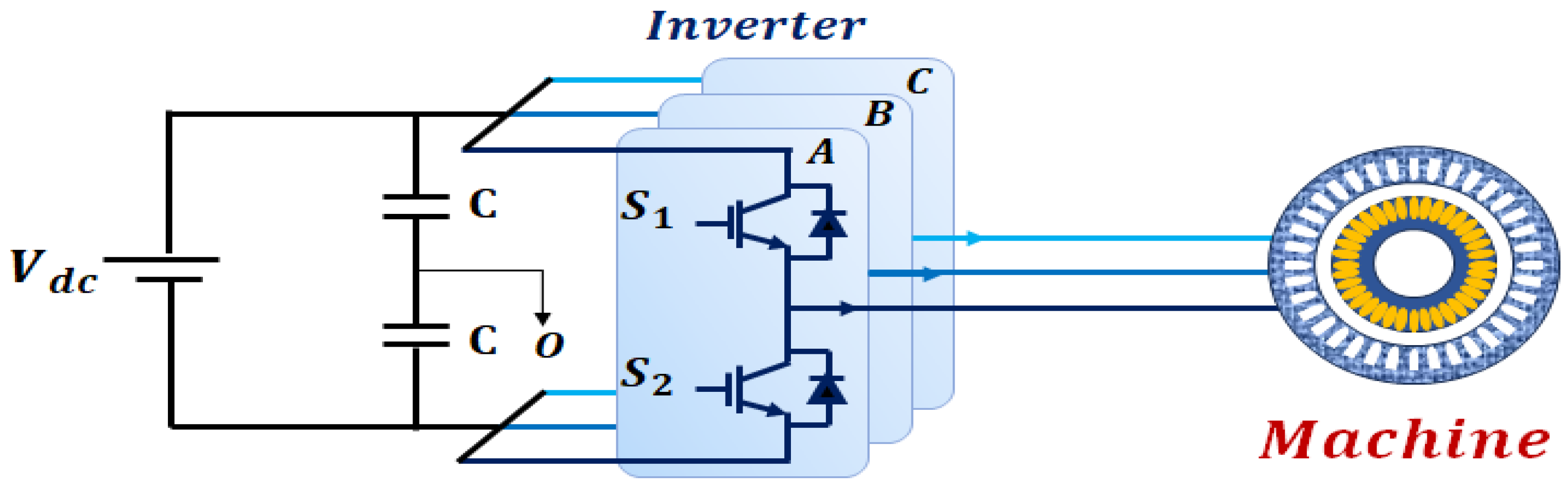
2. Study System Definition and Operating Principle
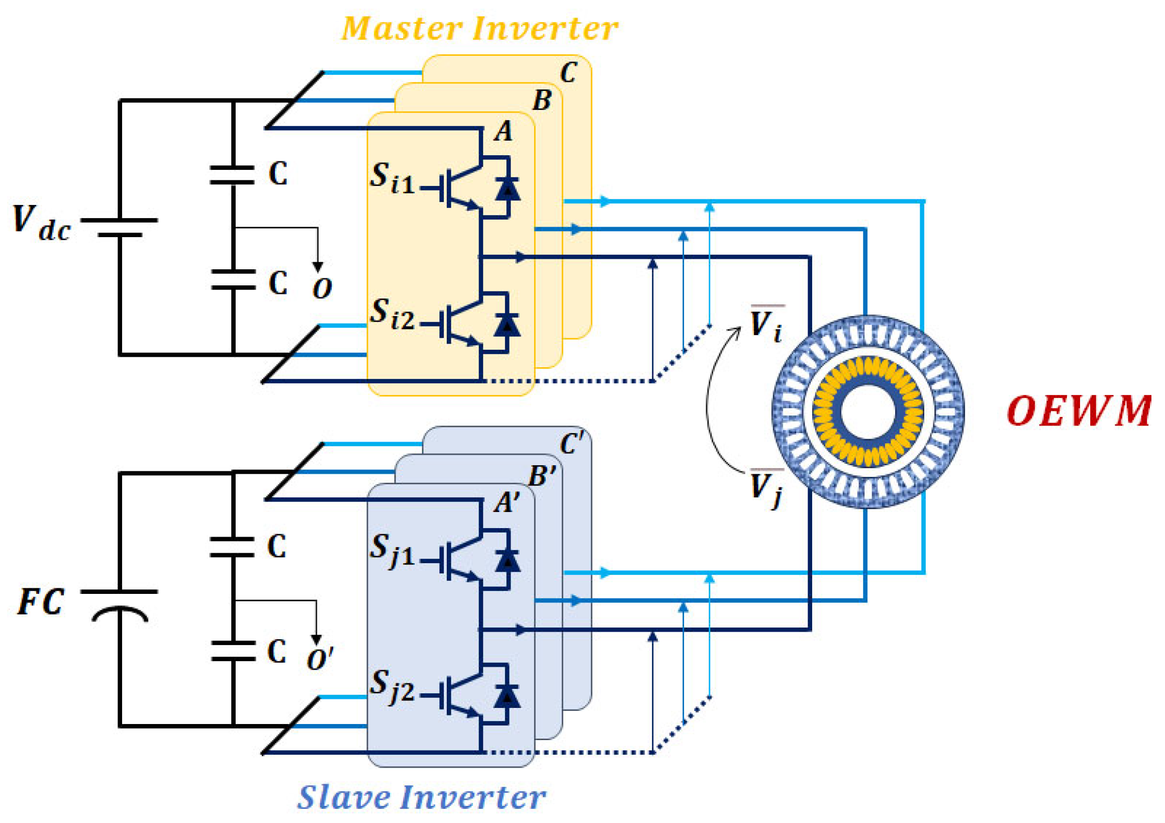
The basic principle of the DTLI configuration is to supply the stator using two separate inverters instead of coupling it in a star or delta configuration [
92,
93] (see
Figure 2). In this configuration, each side of the stator is powered by a dedicated inverter (see
Figure 3). This approach has gained popularity in various modern applications due to its advantages [
49,
50,
51,
53,
54].
This structure consists of two two-level inverters, referred to as inverter
i (Master inverter) and inverter
j (Slave inverter), respectively. The voltage vectors in an
reference frame for each inverter (
and
) can be calculated as follows [
94]:
where
,
is the DC bus voltage, and
and
represent the switching states of inverters
i and
j, respectively.
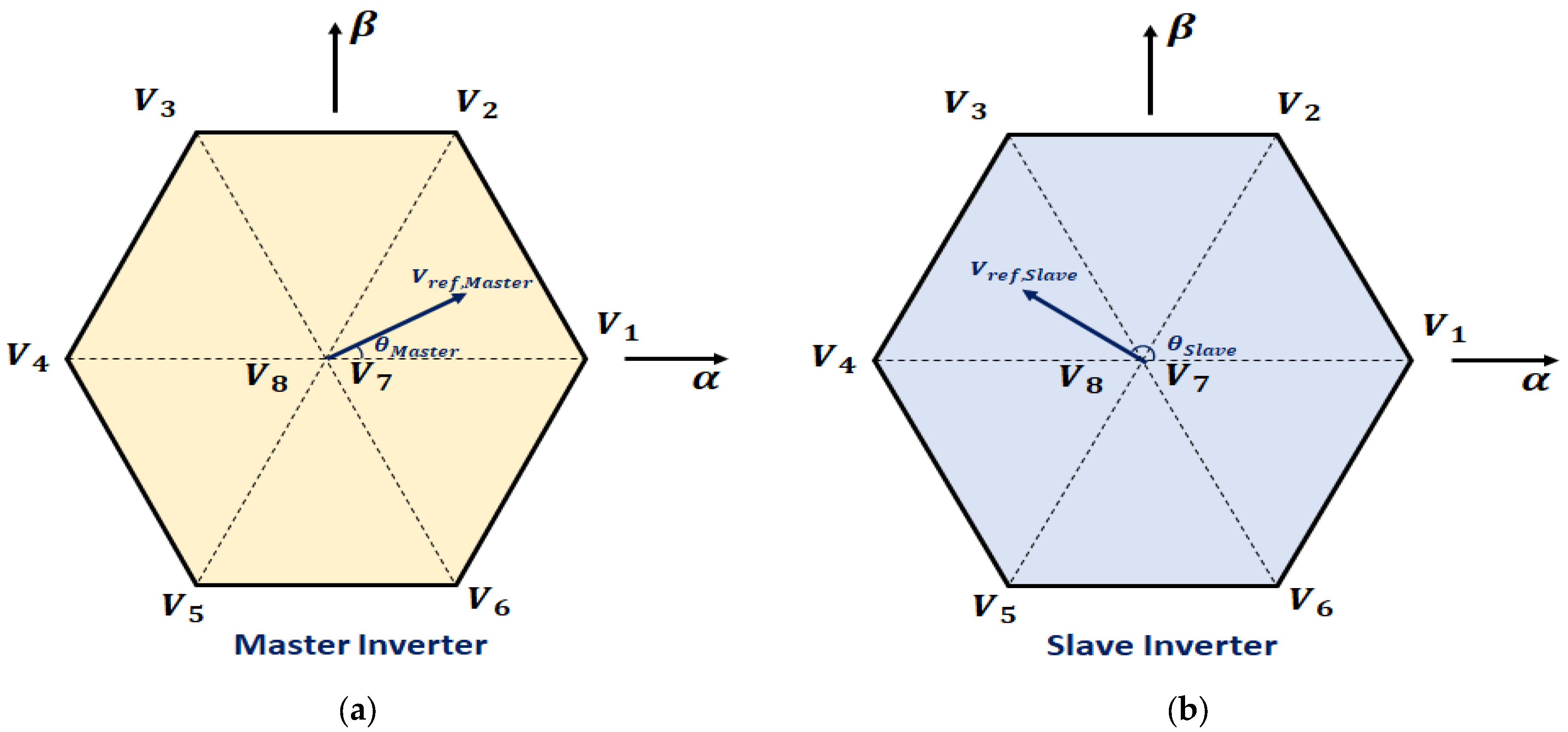
As highlighted in the study of [
95], the operating principle of the DTLI structure relies on the coordinated synthesis of voltage vectors from both inverters to generate the rotating magnetic field required for motor operation. In a symmetric configuration, when the Master and Slave inverters apply identical voltage vectors simultaneously, their resulting magnetic fields tend to cancel each other out. This cancelation disrupts the formation of the rotating field, potentially causing the motor to stop. To overcome this limitation, asymmetric control strategies are employed. These strategies introduce a phase shift between the voltage vectors generated by the Slave inverter relative to those of the Master inverter, ensuring constructive vector interaction, effective field generation, and sustained motor operation.
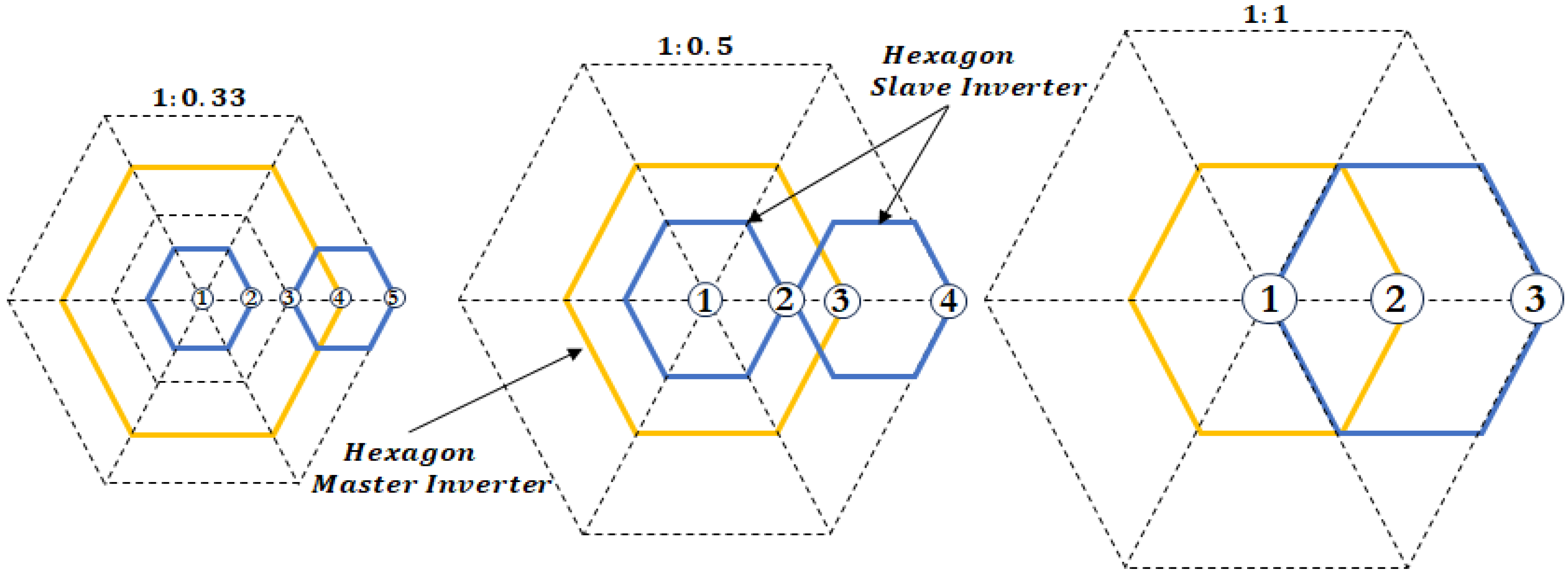
Figure 4 illustrates the hexagon formed by the eight voltage vectors generated by Equations (1) and (2). Within this hexagon, each inverter generates six active vectors and two zero vectors. The values “1” and “0” correspond to the on and off states of the inverter switches, respectively.
Considering the circuits
,
, and
in
Figure 3, the three-phase voltages
,
and
can be expressed using Kirchhoff’s law, as shown in Equation (3):
where
,
,
and
,
,
represent the three-phase pole voltages of the master inverter and the slave inverter, respectively.
Assuming that the three-phase loads are symmetrical, the sum of the load phase voltages must be zero, as expressed in Equation (3).
Thus,
can be obtained by summing the three equations in (3), leading to Equation (5).
By substituting Equation (5) into Equation (3), the phase voltage expression is updated as follows:
From Equation (6), it can be observed that the phase voltage
applied by the DTLI to the OEWM in
Figure 2 corresponds to the voltage difference between the two inverters,
and
. Thus,
can be expressed by Equation (7) [
96].
In the power circuit configuration of the three-phase inverters shown in
Figure 3, the two switches in each inverter leg operate in a complementary manner, meaning that, when one switch is turned on, the other is turned off. By utilizing this switching behavior, the phase output voltages of each inverter, referenced to the negative terminal of the DCB, can be expressed in matrix form as follows:
As presented in Equation (7), the phase voltages applied by the DTLI to the OEWM are obtained by computing the difference between the output voltages of the two inverters. This relationship can therefore be modeled by the following equation, which yield
Based on this principle, the space vector diagram of a DTLI can be represented in
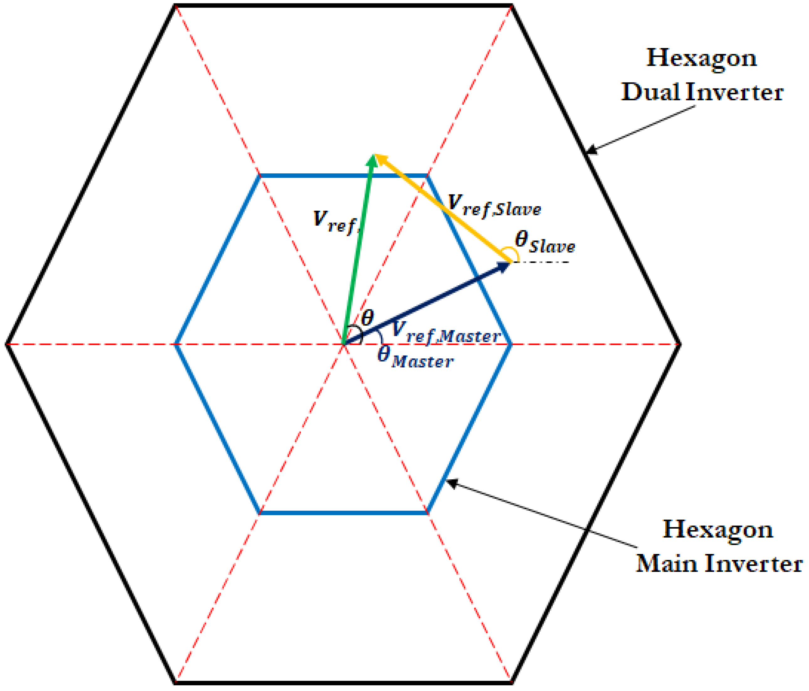
Figure 5, where the hexagonal space vector set generated by the slave inverter ‘orbits’ around the hexagon of the master inverter.
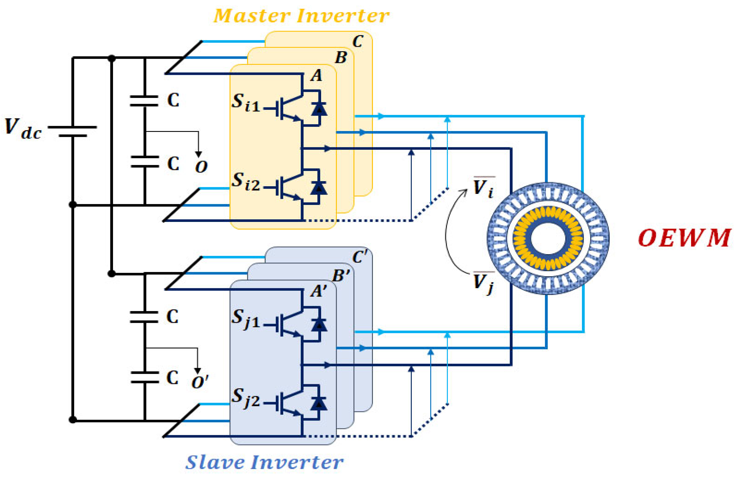
3. Various System Configurations Studied
In the literature, three different types of system configurations powered by two inverters are identified (see
Figure 6): (i) a single common DCB source, (ii) two isolated DCB sources, and (iii) a single DCB source with a floating capacitor.
3.1. Configuration Type I: A Single Common DCB Source
The DTLI drive circuit configuration powered by a single common DCB source (Type I) is shown in
Figure 7, where a two-level voltage inverter is connected to each side of the OEWM.
Consequently, the DTLI configuration uses twelve semiconductor switching devices (typically IGBTs or MOSFETs) and twelve antiparallel diodes. This configuration relies on the combination of the space vectors from both inverters, resulting in 64 (
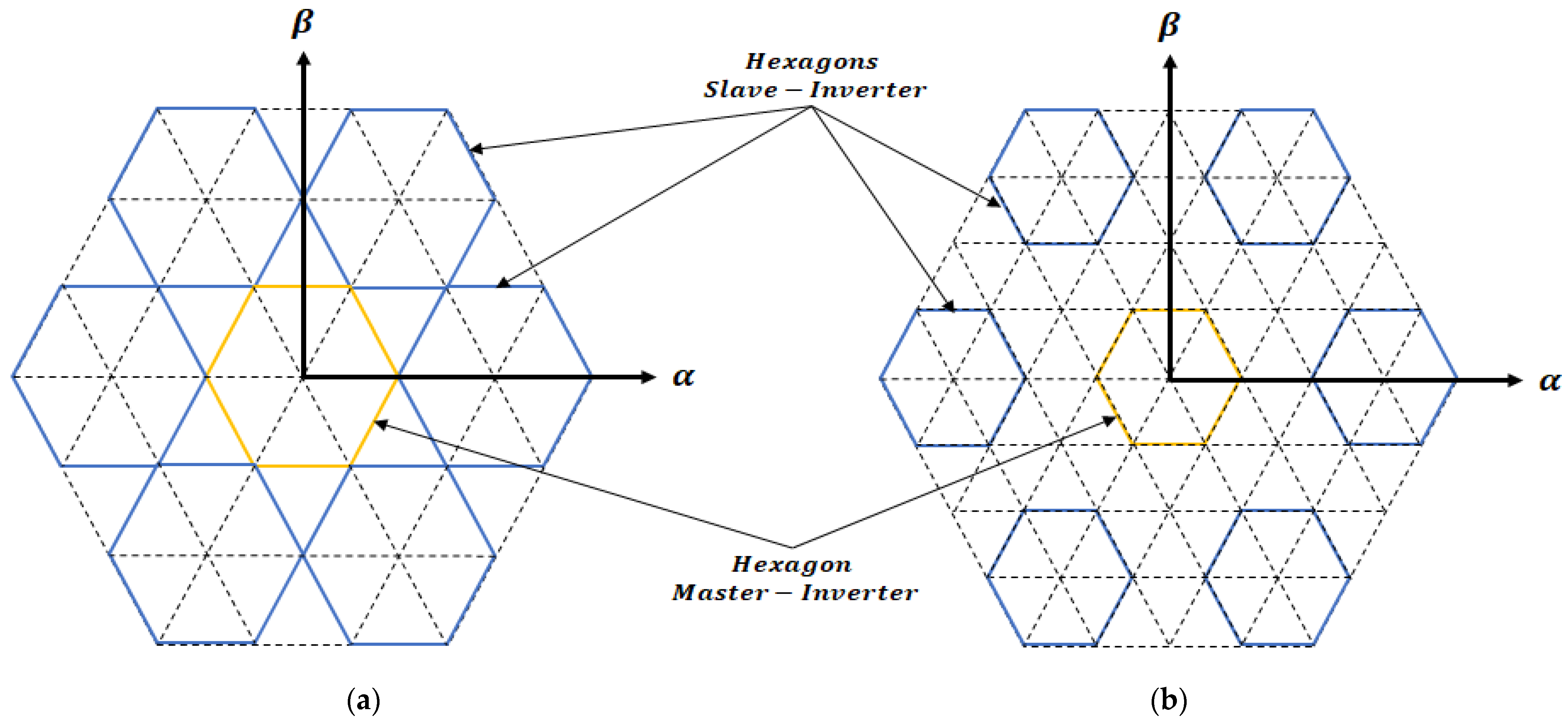
) possible switching combinations distributed across 19 distinct spatial locations. In this configuration, the set of space vector hexagons generated by the slave inverter ‘orbits’ around the space vector hexagon of the master inverter. This DTLI configuration is similar to that of a three-level inverter, as shown in
Figure 8. It consists of three hexagons with vertices of different lengths: a vertex of length
(hexagon ABCDEF), a vertex of length
(hexagon HJLNQS), and a vertex of length
(hexagon GIKMPR).
Table 2 summarizes the classification of these three hexagons into different vector groups.
However, the DTLI configuration powered by a single DC bus source inherently leads to the presence of ZSV, resulting in excessive current and voltage THD. This phenomenon results in high losses, increased temperature, and undesirable vibrations within the machine [
97]. Additionally, this configuration is also affected by the presence of CMV.
3.2. Configuration Type II: Two Isolated DCB Sources
This topology is the same as that described in
Section 3.1. However, it is based on the use of two isolated DCB sources (Type II), as shown in
Figure 9.
This configuration can be divided into two categories: DTLI configurations with symmetrical and asymmetrical voltage sources.
As shown in
Figure 9, this configuration features two separate DC buses, which are mutually isolated [
55,
57,
91,
96,
98,
99,
100,
101,
102,
103,
104,
105,
106,
107,
108]. The isolation of the DC buses prevents the circulation of triple-harmonic currents.
The use of the DTLI system, with two DCB sources of unequal values (asymmetrical voltage source), leads to a significant change in the converter operation, compared to the scenario where both DCB sources have equal values (symmetrical voltage source).
Figure 10 illustrates the voltage vector generation diagrams for these two cases: one with equal voltage sources and the other with unequal voltage sources
.
The vector voltage diagrams are derived by considering the complex switching sequences
and
. These sequences are defined for the master inverter
and for the Slave inverter
, as shown in
Figure 3. The output voltages are given by Equation (11), and the corresponding diagrams are provided in
Figure 10.
The complex vectors resulting from various switching combinations are used to indicate the direction of the complex voltage vectors’ positions. In this context, there are two voltage vectors: one aligned with the “
” axis and the other 60 degrees out of phase with the “
” axis. The amplitude of the voltage vectors is determined by the electrical source value. If the two voltage sources are of equal intensity, the corresponding voltage vectors will have the same magnitude and orientation. However, if the voltages are unequal, such as in a
voltage ratio, additional vectors are generated. These extra vectors can be observed in
Figure 10. Further analysis shows that some of these additional vectors may be redundant. By employing asymmetrical voltage sources, these redundant vectors can be isolated, increasing the number of available output voltage vectors. This provides a broader range of options for generating distinct output voltages.
Figure 11a illustrates a spatial vector scheme for a two-level DTLI, utilizing voltage sources with an unequal voltage ratio of
. This converter system, with a
voltage ratio, generates 37 voltage vectors, which are uniformly and symmetrically distributed in the
plane.
On the other hand, the vector diagram shown in
Figure 11b is constructed considering the use of asymmetrical sources with a voltage ratio of
. In this converter configuration, 48 voltage vectors can be generated. However, these vectors are distributed asymmetrically in the
plane. It should be noted that, in this arrangement, certain areas present challenges regarding the selection of the three closest vectors. This complexity may introduce additional harmonics into the output waveform. Furthermore, in this configuration, the number of redundant states is minimized. As a result, at lower modulation levels, the inverter may cause the overcharging of low-voltage capacitors in specific regions.
The main drawback of this configuration with two iso-linked DC bus sources is the risk of overcharging the DC buses. To prevent this issue, additional components must be integrated.
3.3. Configuration Type III: A Single DCB Source with an FC
This configuration is similar to the one described in
Section 3.1. However, a key difference is that, in this structure, the slave inverter is supplied by a floating capacitor (Type III) instead of a DCB source. This distinction is illustrated in
Figure 12.
In the DTLI with an FC, as illustrated in
Figure 12, the voltage ratio between the DCB sources is defined as
, where
is a constant coefficient. In this setup, the master inverter is supplied with a fixed DCB voltage
, while the Slave inverter is powered by a floating capacitor that provides a voltage of
. The capacitor is connected without a fixed reference point, and its voltage is naturally self-balanced based on the system configuration and the applied control strategy.
During the modulation process, the phase currents can flow through the FC, resulting in voltage fluctuations across it. By convention, a current flowing into the Slave inverter is considered positive, and the switching states of the Slave inverter directly influence the current through the capacitor.
Since a single modulation vector can be synthesized from multiple switching states, these vectors can be categorized based on their impact on the current flowing through the FC as follows:
- -
Type 1 vectors: These vectors induce two opposite current flows within the same phase, such as positive and negative currents in phase , depending on the specific switching states.
- -
Type 2 vectors: These vectors result in current flow in only one direction within a given phase, for example, only a positive current in phase .
- -
Type 3 vectors: These vectors produce no current flow through the FC, regardless of the switching states.
- -
Type 4 vectors: These vectors generate current flow in different phases, such as a positive current in phase in one state and a negative current in phase in another.
This classification offers valuable insight into the interaction between modulation vectors and the dynamic behavior of the FC. A more detailed example of the application of these principles is provided in
Section 5.
This configuration combines the advantages of the other two setups, offering multilevel output voltage and voltage amplification capabilities, thanks to the elimination of ZSV circulation. Additionally, it eliminates the need for an isolation circuit, as one of the inverters is floating.
In this DTLI configuration with an FC, the main challenge is regulating the FC voltage to the desired value. Likewise, in DTLI systems with isolated asymmetrical power supplies, a potential concern is that the capacitor on the low-voltage side may be overcharged due to energy flow from the high-voltage side.
In summary, each of the three DTLI configurations presents distinct characteristics in terms of performance, complexity, and implementation requirements. The Type I configuration stands out for its structural simplicity and ease of implementation. However, it is affected by the generation of CMV and ZSV, which can degrade the output voltage quality and increase the overall system losses. The Type II configuration eliminates these undesirable effects and enhances modulation flexibility, especially when asymmetric voltage sources are used. On the other hand, the need for galvanic isolation adds to the cost and increases the risk of capacitor overcharging on the lower voltage side. The Type III configuration offers a good compromise by combining the benefits of the two previous structures while eliminating the need for isolation. Nonetheless, it introduces a challenge in regulating the voltage across the floating capacitor, particularly in transient operating conditions. Therefore, the selection of the most appropriate configuration should be guided by the specific requirements of the application, including cost constraints, control complexity, and desired output voltage quality.
6. Various Criteria for Assessing the Power Quality and Efficiency of the Studied System
The deployment of DTLI configurations offers promising prospects across a wide spectrum of power electronic applications. Nevertheless, each configuration presents a unique set of technical challenges that must be addressed to ensure optimal operation and achieve the desired performance.
In this context, we examine the challenges associated with three distinct DTLI architectures, whose difficulties stem from their specific characteristics, ranging from complex voltage modulation to the management of asymmetrical power sources.
A comprehensive understanding of these constraints is crucial to fully harness the benefits provided by the various DTLI topologies. These challenges can broadly be classified into two categories: those related to power quality and those concerning energy efficiency.
6.1. Power Quality
Electrical power quality has become a critical factor in the design and operation of power systems and electrical machines. This subject has garnered considerable interest from both academic researchers and industrial practitioners, leading to the publication of numerous works in this dynamic and relatively recent field [
132].
Power quality encompasses several key issues, such as voltage dips, outages, harmonics (notably THD), over-voltages, unbalances, and voltage fluctuations, among others.
With the introduction of new converter configurations, two additional quality concerns arise: common-mode voltage and zero-sequence voltage.
This study addresses a range of quality-related challenges, including harmonic distortion, common-mode voltage, zero-sequence voltage, DC bus overcharging, and the regulation of floating capacitor voltages.
6.1.1. THD
In systems associated with power converters, output voltage/current quality is closely linked to THD. The IEEE Std 519-1992 standard recommends harmonic control requirements for electrical systems [
133].
By definition, THD characterizes the effects of harmonics on power system voltage and can be applied to low-, medium-, and high-voltage systems [
133]. The THD is defined by Equation (14).
where
is the harmonic order,
is the amplitude of the harmonic component, and
is the amplitude of the fundamental component.
The IEEE Std 519-1992 standard defines voltage distortion limits at the Point of Common Coupling (PCC) and requires that customers do not introduce excessive current harmonics [
133]. For systems where the bus voltage at the PCC is less than or equal to 69 kV, individual voltage distortion must remain below 3%, and the THD must not exceed 5%. The Fast Fourier Transform (FFT) can be used to perform a spectral analysis of electrical signals and thus serves as an effective tool for THD evaluation [
134].
6.1.2. Common-Mode Voltage (CMV)
In three-phase sinusoidal power systems, balance and symmetry are fundamental under normal operating conditions. The phase voltages naturally compensate each other, and grounding the source’s neutral point reinforces this symmetry.
However, when a three-phase pulse width modulation (PWM) inverter is employed, the switching of asymmetrical voltages introduces a DC voltage (
) across the load phases. This deviates from the ideal sinusoidal behavior, as the instantaneous sum of the load terminal voltages is no longer zero. This deviation leads to the emergence of CMV between the load and ground [
135].
CMV results from the high-frequency switching of inverter devices. The common-mode currents induced between the stator windings and ground can have serious consequences, such as premature bearing degradation, increased thermal losses, and an overall decline in motor performance [
73].
The CMV generated by the inverter can be expressed by the following equation [
136]:
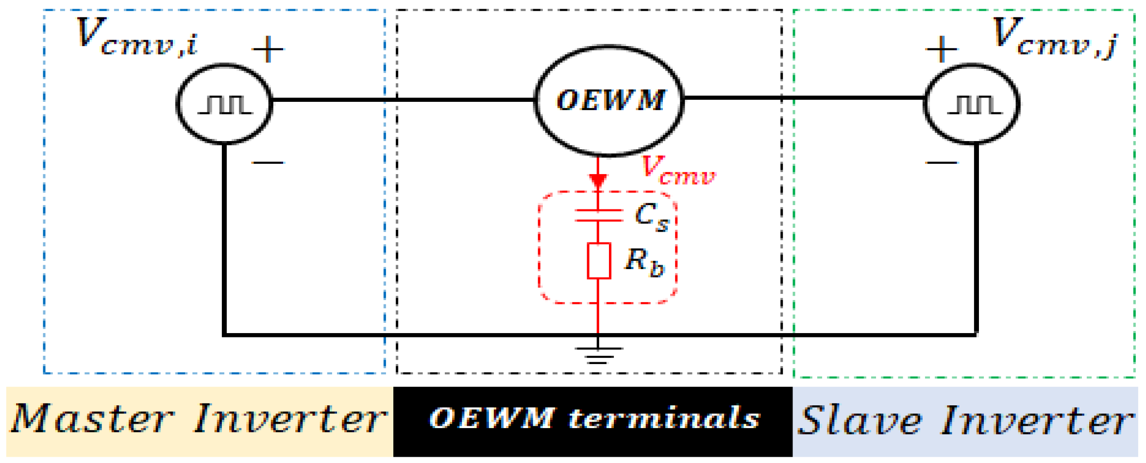
In DTLI systems, like the one shown in
Figure 5, the CMV for each inverter can be calculated using the formulas provided in the study of [
58]:
Consequently, the CMV of DTLIs can be calculated as follows [
137]:
In the context of DTLI systems, CMV-related issues become more critical due to the frequent high-frequency switching of the inverters’ switches. This rapid switching can shorten motor life and increase the risk of inverter failure. Moreover, the impact of these issues is amplified by factors such as shaft voltages, bearing currents, and electromagnetic disturbances caused by common-mode leakage currents [
138].
The effects of CMV on the system are primarily influenced by the parasitic parameters between the motor and ground. Among these, parasitic capacitance
and parasitic resistance
are crucial in the generation of bearing current, an undesirable component that can negatively affect the system’s performance. A schematic diagram (
Figure 16) effectively illustrates how these parasitic parameters contribute to bearing current generation in response to CMV.
One of the key advantages of a DTLI connection is its ability to attenuate CMV, thereby mitigating the problems associated with it. The combination of spatial vectors resulting from the use of DTLIs leads to a variety of CMV levels, as thoroughly demonstrated in
Table 3. From this table, it is evident that large vectors (such as
,
,
,
,
,
) and zero vectors (
,
,
) effectively eliminate CMV. On the other hand, zero vectors (
,
) and intermediate vectors (
,
,
,
,
,
,
,
,
,
,
,
) generate varying levels of CMV.
Various approaches have been developed to mitigate CMV, including the use of passive and active common-mode filters [
139,
140,
141,
142]. However, the implementation of these devices introduces additional costs and significant power losses. As a result, PWM methods have become the preferred solution for two-level inverters, though they do not fully eliminate CMVs [
143,
144].
In a previous study [
145], an approach was presented that exclusively uses even or odd space vector combinations to reduce CMV from
to
, without relying on null vector states, within a conventional two-level inverter. Additional modulation-based strategies have been developed to eliminate common-mode voltages by using only a specific subset of the output space vectors [
146,
147]. However, these methods face a limitation regarding the maximum phase voltage, which restricts the optimal use of the DC bus voltage.
6.1.3. Zero-Sequence Voltage (ZSV)
It is widely recognized that unbalanced three-phase voltages can be decomposed into three distinct sets of voltage components [
126]. These components, known as “symmetrical components,” are classified into positive sequence, negative sequence, and zero sequence. Their schematic representation is shown in
Figure 17a. The positive and negative sequence components represent three-phase, rotationally balanced phases, while the zero sequence components correspond to a phase with a zero-phase angle. To provide a clearer understanding of this decomposition,
Figure 17b illustrates how an unbalanced three-phase voltage breaks down into its symmetrical voltage components.
Unlike positive and negative sequence currents, zero-sequence currents present a unique challenge. Unlike the former, which compensate for each other, zero-sequence currents add arithmetically at the neutral point of a three-phase, four-wire system. This accumulation can lead to the overloading of the neutral conductor or cause a higher voltage between neutral and earth. Additionally, harmonic currents of any sequence flowing through an AC drive can increase the RMS current, resulting in higher system losses, increased THD for current or voltage, and potential overheating and vibration issues in the machine [
135].
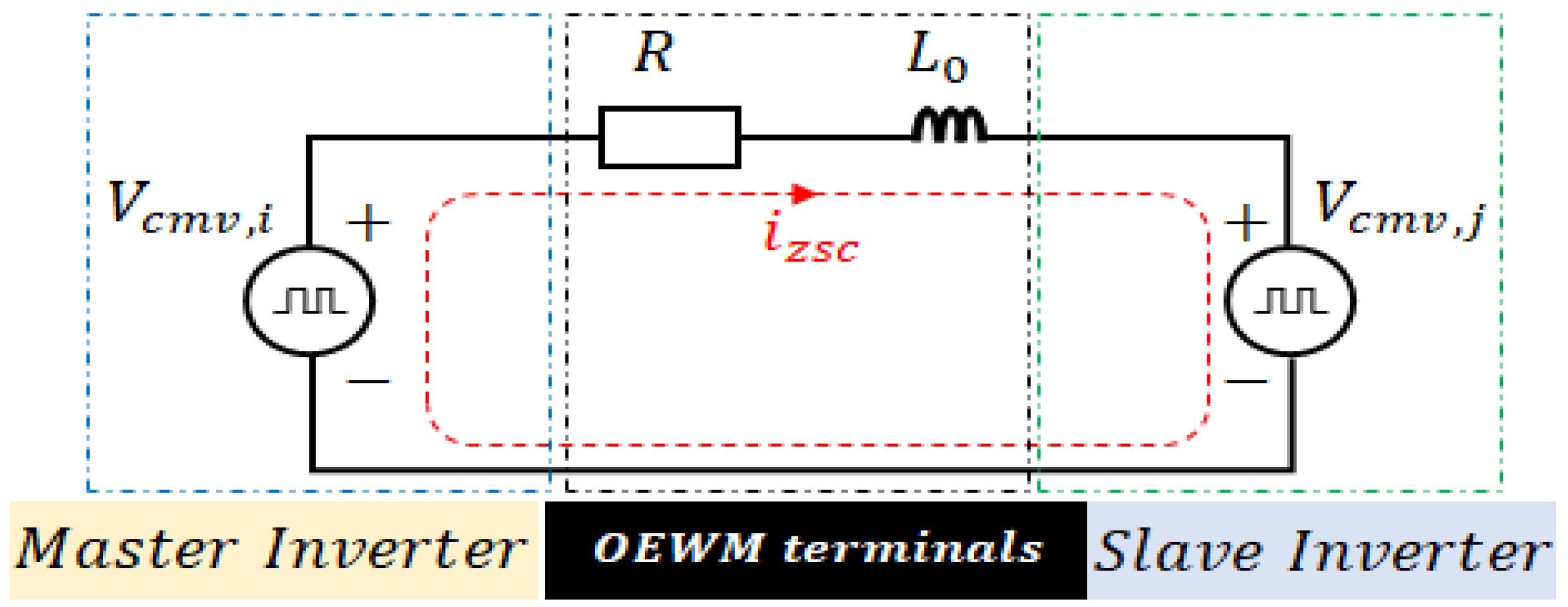
In a DTLI-powered configuration with a single DCB source, zero-sequence currents (ZSCs) can occur due to ZSV. This voltage arises from the asymmetry of the instantaneous pulse width modulated phase voltages applied to the machine windings, which results from the use of spatial voltage vectors. The corresponding equivalent diagram of the zero-sequence loop is shown in
Figure 18. In this diagram,
represents the inductance of the homopolar sequence,
is the resistance of the phase winding, and
and
are the CMVs generated by the two inverters in the system, respectively.
The ZSV can be expressed in terms of the CMV of each inverter
as follows [
62]:
In the DTLI configuration, the ZSV resulting from the 64 space vector combinations can be calculated using Equation (21), as shown in
Table 4. From
Table 3, it is clear that the zero vectors (
,
) and the intermediate vectors (
,
,
,
,
,
,
,
,
,
,
,
) eliminate the ZSV. Conversely, large vectors (
,
,
,
,
,
) and zero vectors (
,
) generate various levels of ZSV.
Table 3 and
Table 4 demonstrate that vectors generating ZSV effectively eliminate CMV. In contrast, vectors designed to eliminate ZSV inevitably introduce CMV. These results highlight the complex interplay between the vectors responsible for both generating and reducing the CMV and ZSV components.
The ZSV issue generates ZSCs, leading to the presence of triple current harmonics [
137]. This current can be harmful to motor windings, resulting in increased copper losses and potential circuit saturation. Several methods have been proposed to eliminate this voltage in DTLI configurations. In [
148], the solution involved integrating auxiliary switches, while, in [
91], an approach was suggested where one side of the OEWM is fed by a three-level inverter, and the other side is fed by a two-level inverter. However, these solutions require additional hardware, which increases costs. Therefore, a more cost-effective solution would be to design appropriate control strategies to eliminate the ZSV. For instance, in [
149], the authors proposed desynchronizing the control between the two inverters to create a 120° phase shift between the voltages of the first and second inverters. Similarly, the authors of [
150,
151] employed a 180° phase shift and introduced the use of even or odd synchronous vectors. In [
152], two approaches were suggested that allow for free selection of DTLI switching states. However, these approaches not only eliminate the ZSV but also restrict the inverter switching. Finally, the authors of [
48,
153] developed a technique called Decoupled Sample-Averaged Zero-Sequence Elimination, which forces the ZSV to zero while minimizing switching losses. A new method tailored for low switching frequencies, called Synchronous Off-Line Optimum PWM, was presented in [
154].
6.1.4. DCB Overcharging
DTLI configurations, supplied by two isolated and symmetrical voltage sources (with a voltage ratio of
, i.e., both converters use the same voltage level), designed to improve output voltage quality by enabling three-level operation, represented a significant advance in terms of output voltage quality [
155].
However, to further improve voltage quality, configurations with two isolated but asymmetrical voltage sources (with a voltage ratio of
) were introduced, allowing a four-level operation [
67]. However, the use of these asymmetrical sources introduced a potential overcharging problem, particularly at the DC bus capacitor (DCB-C) (see
Figure 19).
The overcharging problem is related to the phase current flowing in the DCB-C during the modulation process. This current is made up of the components
,
, and
, as shown in
Figure 19. Depending on the specific switching states, these currents can cause the DCB-C to overcharge. To better understand these scenarios,
Figure 20 shows different cases of current flow in the DCB-C, using colors to indicate the path of phase current flow. Green represents the
current, red the
current, and blue the
current.
For example, in
Figure 20a, current
acts on the positive pole of the DCB-C for the switching state
. However, for the switching state
, shown in
Figure 20b, no current flows through the DCB-C.
Figure 20c,d show the current flows resulting from switching states
and
, respectively. In the case of the
state, the
current flows in the positive polarity of the DCB-C, while, for the
switching state, it flows in the negative polarity of the DCB-C. These currents are referred to as
and
, respectively.
When addressing the issue of overcharging in DTLI systems, the literature typically presents two main approaches. The first approach involves adjusting modulation schemes [
67,
116,
118,
129,
131,
156], while the second involves the use of additional hardware [
113,
117,
119,
130].
In the first approach, switching states are selected by analyzing the current associated with these states to identify those that are likely to cause overcharging. These problematic states are then avoided during the modulation process. This method of voltage regulation, which assumes the direction of the load current, is referred to as the passive regulation method [
157]. However, the disadvantage of this approach is that it reduces the number of vectors available for modulation, which can negatively impact the quality of the output voltage. A strategy to switch the master inverter while keeping the slave inverter engaged is presented in [
118], but this approach involves a larger modulation area, which may result in higher harmonic distortion in the inverter output. To improve power quality, a coupled discontinuous carrier modulation technique is proposed in [
129], but this can increase switching losses. A significant limitation of passive control is that it assumes the direction of current, which can be affected by the power factor of the load [
157]. An enhanced version of passive control, called active control, was proposed in [
156]. This approach actively selects the appropriate states based on control requirements and measured phase current values.
The second approach, which utilizes additional hardware, is based on the nested rectifier–inverter structure proposed in [
117] (see
Figure 21) and further refined in [
158]. In this structure, the slave inverter with a lower DCB voltage is nested inside a higher-voltage DCB feeding the master inverter. This configuration enables the implementation of advanced modulation schemes to optimize voltage utilization for motors [
119] or to suppress ZSCs in an averaged manner [
130].
It should be noted that, while the nested rectifier–inverter configuration can address the overcharging problem, it requires an additional isolated DC power supply. This addition can lead to increased complexity, size, and cost of the motor drive system [
118,
129].
6.1.5. Floating-Capacitor (FC) Voltage
Compared to other DTLI configurations, whether with isolated or shared continuous buses, the structure based on a continuous bus and an FC has the notable advantage of minimizing the circulation of ZSVs (ZSCs), which is virtually nonexistent, and does not require additional isolation circuits. However, this approach is not without significant challenges. The main obstacle it faces lies in FC voltage management, which, due to its floating nature [
119], generates undesirable voltage steps at the converter output.
As a result of the voltage control approach applied to both converters, the voltage across the load becomes unpredictable. These unwanted voltage steps have the potential to significantly degrade output performance, thereby reducing the attractiveness of this configuration [
120]. For example, in the case where the voltage ratio is
,
Table 5 presents the 37 space vectors that will charge or discharge the FC and generate a voltage variation. These vectors can be classified into three types: Type 1 for vectors with redundancy states that cause the phase current to act on both the positive and negative polarities of the FC, Type 2 for vectors that have only one instance of current flow, and Type 3 for vectors that have no effect on the voltage variation in the FC.
The authors in [
121,
125] addressed the issue of FC voltage regulation in a DTLI while maintaining multilevel operation. Several approaches were examined:
Coupled Modulation [
121,
123,
124,
125,
128,
159]: This method treats the DTLI as a single unit for modulation, enabling analysis of the switching states’ impact on the capacitor voltage in steady-state operation. However, there is a risk of under-utilizing the capacitor voltage, which can reduce the output level.
FC Voltage Regulation with Reference to Motor Power Factor [
121]: This method involves feedback from the motor power factor angle for regulation, providing an active yet complex solution based on motor speed.
Decoupled Modulation [
65,
122,
160,
161,
162,
163]: In this approach, the FC is treated as a reactive power capacitor, and active power regulation is applied to the FC. However, it may lead to undesirable voltage steps that affect output performance.
Step Modulation for the Master Inverter and High-Frequency PWM for the Slave [
164]: In this scheme, the master inverter operates at the fundamental frequency, while the slave inverter uses high-frequency modulation. The FC voltage is regulated by adjusting the trigger angle of the fundamental voltage. While this approach reduces switching losses, it may not be suitable for all situations and is relatively complex.
6.2. Energy Efficiency: Power Losses
Generally, there are two types of losses in PWM power electronics converters: conduction losses
and switching losses
, with switching losses occurring during the transitions from
to switch-on and from
to switch-off. These losses are expressed as follows [
75]:
where
is the instantaneous phase current,
is the switch-off voltage,
and
are the switch-on and switch-off times,
is the voltage drop,
is the on-time, and
is the switching frequency.
It is well established that, in power semiconductor devices, power losses due to switching are directly proportional to the switching frequency. These switching-related losses occur during the turn-on and turn-off phases of the device and are mainly influenced by the time over which the switching voltage and current rise and fall, respectively [
165]. In other words, as the switching frequency increases, the power losses generated by switching also increase. These losses are primarily determined by the variations in voltage and current during these phases.
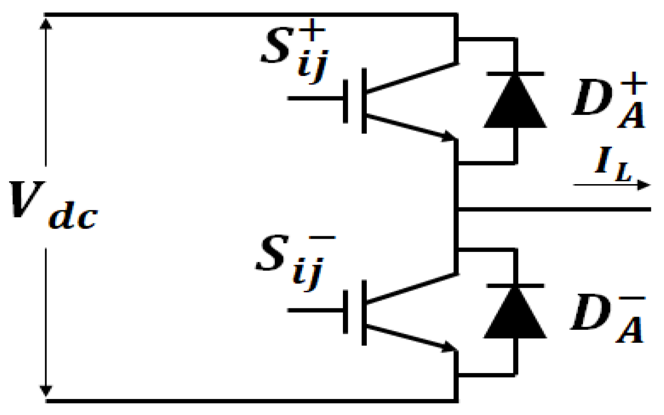
As an example,
Figure 22 illustrates phase A of an inverter arm. In this diagram, components
and
represent the upper and lower switches of the arm, while
and
are the associated antiparallel diodes. Furthermore,
Figure 23 shows the voltage across the switch and the antiparallel diode, as well as the current flowing through them and the resulting power losses, particularly when
.
However, the introduction of DTLIs into a system can negatively impact its overall efficiency, primarily due to the increased power losses they generate. In the context of our configuration, it is important to highlight that total switching losses are significantly higher, potentially reaching up to twice the levels observed in conventional systems [
97].
To increase the efficiency of DTLI systems, various modulation strategies have been explored in the literature. In references [
91,
151,
152,
166], the sub-hexagonal center PWM (SHCPWM) modulation scheme, based on PWM pulse shifting, has been developed to mitigate switching losses. This method involves sequential switching of the two inverters, effectively halving switching losses compared to conventional DTLI configurations. Additionally, SHCPWM avoids the generation of unwanted bearing currents [
91]. However, it is limited by a restricted set of switching states and requires complex PWM pulse reordering, which can be computationally intensive [
91,
151,
152,
166].
Another approach to minimizing switching losses is discontinuous pulse width modulation (DPWM), as described in [
118,
167,
168]. DPWM holds certain power semiconductors in the ON or OFF position over specific intervals. This technique is more efficient than space vector PWM (SVPWM) for high-power, high-frequency switching applications [
59]. Furthermore, different DPWM variants, such as DPWM 30°, 60°, and 120°, have been developed, which reduce switching losses by an average of 33% by avoiding switching transitions near phase current peaks [
169]. DPWM also accounts for the phase difference between current and voltage, even when the power factor is considered [
170].
7. Impact of Control Strategies on OEWM-DTLI Performance
As previously mentioned, the OEWM system is powered by a DTLI, and its modeling is similar to that of a conventional AC machine. In terms of control, two complementary levels of strategies can be identified in the literature: high-level control techniques, which focus on the regulation of machine variables (such as scalar control, vector control, and direct torque control (DTC)), and low-level control techniques, which deal directly with the generation of the modulation and carrier signals, typically based on PWM.
Given our focus on voltage quality and energy efficiency, we concentrate on the PWM control of both inverters. Thus, the performance of the OEWM largely depends on how these two inverters are modulated to produce the appropriate output signals.
To provide an overview of the existing literature,
Table 6 presents a summary of the three types of configurations studied, highlighting their key contributions and their significant effects on OEWM performance. These contributions are particularly notable for their substantial improvements in critical performance parameters, including overcharging of the capacity, CMV, ZSV, THD, and the efficiency of the DTLI system.
8. Conclusions
This paper presented a comprehensive technical analysis of Dual Two-Level Inverter (DTLI) topologies for motor drive applications. The investigation covered the fundamental operating principles of DTLI systems and examined three key structural configurations: the conventional Common DC Bus (C-DCB), the Two-Isolated DC Bus (TI-DCB), and the more recent Floating Capacitor-based DC Bus (DCB-FC). A detailed mathematical model of the DTLI system was developed to support this analysis, highlighting voltage distribution mechanisms and control strategies specific to each architecture.
To evaluate system performance, several critical criteria were considered, including total harmonic distortion (THD), common-mode voltage (CMV), zero-sequence voltage (ZSV), energy efficiency, floating capacitor voltage behavior, and the risk of DC bus overcharging. In addition, this study included a comparative summary (
Table 6) of several PWM techniques, emphasizing their influence on waveform quality and overall system efficiency across the three configurations.
Among the architectures studied, the dual C-DCB configuration stood out for its simplicity and robustness, attributed to its symmetrical design and straightforward control implementation without the need for additional hardware. However, its limitations in suppressing ZSV, alongside the DC bus overcharging risks associated with the TI-DCB configuration, motivated further interest in the DCB-FC structure. The DCB-FC demonstrated superior performance thanks to its self-regulated floating capacitor voltage and the elimination of isolation requirements.
In conclusion, both the C-DCB and DCB-FC configurations exhibit strong potential for modern high-performance power conversion systems, offering practical trade-offs between simplicity, control complexity, and electromagnetic performance. These findings serve as a foundation for the development of more efficient and reliable inverter systems in future industrial and renewable energy applications.


