Abstract
This article presents a throughput/area accelerator for elliptic-curve point multiplication over . To optimize the throughput, we proposed an efficient hardware accelerator architecture for a fully recursive Karatsuba multiplier to perform polynomial multiplications in one clock cycle. To minimize the hardware resources, we have utilized the proposed Karatsuba multiplier for modular square implementations. Moreover, the Itoh-Tsujii algorithm for modular inverse computation is operated using multiplier resources. These strategies permit us to reduce the hardware resources of our implemented accelerator over a large field size of 571 bits. A controller is implemented to provide control functionalities. Our throughput/area accelerator is implemented in Verilog HDL using the Vivado IDE tool. The results after the place-and-route are given on Xilinx Virtex-6 and Virtex-7 devices. The utilized slices on Virtex-6 and Virtex-7 devices are 6107 and 5683, respectively. For the same FPGA devices, our accelerator can operate at a maximum of 319 MHz and 361 MHz. The latency values for Virtex-6 and Virtex-7 devices are 28.73 s and 25.38 s. The comparison to the state-of-the-art shows that the proposed architecture outperforms in throughput/area values. Thus, our accelerator architecture is suitable for cryptographic applications that demand a throughput and area simultaneously.
1. Introduction
Elliptic curve cryptography (ECC) [] and Rivest-Shamir-Adleman (RSA) [] are well-known public-key cryptographic schemes. ECC guarantees comparable security with shorter key lengths compared to RSA. For example, 233 bits of ECC are sufficient to achieve identical security to a 2048-bit RSA []. The low area, low power consumption, and lower channel bandwidth are some benefits of the shorter key lengths when transmitting sensitive information over the unsecured channel. These advantages enable ECC for area-constrained applications such as wireless sensor nodes (WSNs) [,], radio-frequency-identification-networks (RFID) [,], automotive vehicles [], and secure robotics communication [].
The National Institute of Standards and Technology (NIST) (NIST is an American organization that maintains security standards for efficient communications) has standardized ECC for prime and binary fields, i.e., , and []. To implement NIST-recommended prime and binary field lengths, ECC includes four layers of a model []. The topmost layer is the protocol which ensures encryption/decryption, signature generation/verification, key authentication between two devices, etc. The critical operation in ECC is point multiplication (PM). It includes point addition (PA) and double (PD) operations for computations. The PA and PD operations are the layer two operations in ECC. The building blocks of layer one are modular arithmetic operators (adder, square, multiplier, and inversion). The efficiency of the PM operation of ECC relies on the efficient implementations of these modular arithmetic operators.
There are two possible choices to implement ECC either on software platforms (such as microcontrollers) or as hardware accelerators on field-programmable gate arrays (FPGA) and application-specific integrated circuits (ASIC) platforms. The software-ported implementations provide higher flexibility with limited throughput. Hardware accelerators provide higher throughput with limited flexibility features []. Therefore, there is always a tradeoff. ECC suggests prime and binary fields for different implementation platforms (software or hardware). The prior is more advantageous on software platforms, while due to carry-free additions, the binary fields are more appealing for hardware accelerations of building blocks of ECC. To implement prime and binary fields, ECC provides two basis for point representation []: (i) polynomial and (ii) normal. For efficient modular multiplications, polynomial basis representation is more practical. A normal basis is appropriate for frequent modular square implementations [,]. The general affine and projective coordinates influence the performance of the ECC implementations. The affine coordinate is more expensive in computational time as it needs an inversion operation during the execution of each PA and PD operation [,,]. In addition, the affine coordinates are reasonable for software implementations. On the other hand, the projective coordinates are suitable for achieving throughput/area ECC accelerators. Based on the discussions presented above, we have selected: (i) binary fields, (ii) projective coordinates, and (iii) polynomial basis representations because our focus is to accelerate ECC on a hardware platform.
Some recent FPGA and ASIC accelerators of PM computation of ECC over are described in [,,,,,,]. An efficient throughput/area ECC processor over to is presented in []. The authors presented the rescheduling of PA and PD operations to reduce the clock cycles. The decrease in clock cycles eventually reduces the latency (i.e., the computation time). A segmented digit-serial modular multiplier is employed to reduce hardware resources. The implementation results are reported on the Xilinx Virtex-7 FPGA device. Another throughput/area ECC processor is implemented in []. The authors implemented a modular digit parallel multiplier with a digit length of 41-bits to minimize the hardware resources. Moreover, the authors utilized the existing hardware resources of the multiplier to operate the modular square operation of ECC. Towards optimizing the throughput, a 2-stage pipelining is incorporated. Additionally, rescheduling the PA and PD operations is proposed to reduce the clock cycles. The implementation results over to are reported on Xilinx Virtex-7 FPGA. In addition, they implemented their design on ASIC 16nm process technology.
In [], a right-to-left PM algorithm is utilized to achieve the parallel computation of Frobenius maps and point additions. A rescheduling in consecutive point additions is proposed to minimize the latency and maximize the circuit frequency. Moreover, they have utilized a pipelined bit-parallel modular multiplier. The implementation results over to are provided on Xilinx Virtex-5 FPGA. In [], a 6CC-6CC (clock cycle) dual-field PM design is presented. This is achieved with a rescheduling of PA and PD operations of ECC. Additionally, they have utilized multiple Karatsuba-based modular multipliers to reduce the clock cycles.
A physical unclonable function is utilized with ECC to improve the security for IoT devices in []. The hardware resources are minimized by reusing the underlying finite field computing units. Their circuit achieves a maximum of 135 MHz frequency on Virtex 6 FPGA. One PM computation takes 19.33, 22.36, 41.36 and 56.5 s for 233, 283, 409 and 571 key lengths. In [], different digit lengths are applied to the data path of the multiplier and division circuits to explore the resulting performances and find out an optimal digit size. The implementation results are reported on Virtex-5 FPGA for 163, 233, 283, 409, and 571 key lengths. For the identical key lengths, their architecture takes 5.5, 17.8, 33.6, 102.6 and 384 s for one PM computation. A segmented pipelined full-precision multiplier is adopted in [] to reduce the computation time, i.e., latency. Moreover, a Lopez-Dahab Montgomery PM algorithm is modified for careful scheduling to minimize the number of clock cycles.
The PM architectures, described in [,,,,,,], shows that different optimization techniques such as pipelining, parallelism, PA and PD operations of rescheduling, and different modular multipliers, i.e., digit-serial, digit-parallel, and bit-parallel, etc., have been used in the literature to maximize the performance of PM operation. Due to higher area complexity, the PM architectures of [,,,,,] are not suitable for area-constrained applications such as WSNs, automotive vehicles, RFID, etc. Moreover, the higher computation time required in designs of [,] makes these architectures inappropriate for aforesaid applications. Therefore, the objective of this work is to provide a large field-size throughput/area accelerator for PM computation on FPGA. This is achieved with the following novel contributions:
- We present a flexible hardware accelerator of a large field-size PM processor for to optimize the throughput/area utilization. Flexibility means that the users can load different curve parameters and a scalar multiplier to our proposed processor for PM computation (more particular details are shown in Section 3.1).
- To minimize the clock cycle counts, we have implemented a fully recursive Karatsuba multiplier for a binary field of 571 bits. It computes one modular multiplication over two 571-bit inputs in one clock cycle (details are given in Section 3.3).
- To minimize the hardware resources, we have used the Karatsuba multiplier for modular square implementations. Moreover, the Itoh-Tsujii algorithm [] for the modular inverse computation is operated using our multiplier resources.
- A finite-state-machine (FSM)-based controller is implemented to provide efficient control functionalities.
The remainder of this article is structured as follows: Section 2 provides the required mathematical background to implement the ECC PM operation. Our proposed crypto processor architecture design is described in Section 3. The implementation results and comparisons are provided in Section 4. Finally, the paper is concluded in Section 5.
2. ECC Background over
For field, an affine form of ECC is defined as a set of points, i.e., x, and y, by satisfying Equation (1), where x and y present the coordinates of the field. The curve constants are a and b with . An irreducible polynomial is the . The representation of x and y coordinates of the field in a triplet, i.e., X, Y, and Z, are projective coordinates. Therefore, for the field, a Lopez Dahab projective form of Equation (1) is defined as set of points , presented in Equation (2). In Equation (2), the variables X, Y and Z are the Lopez Dahab projective elements of point , where , a and b are the curve constants with the .
The points on the elliptic curve define a group—called an additive group. It means that the ECC points are combined with the point at infinity. Following the additive group definition, adding two elements in a group defines another element in the same group. For example, we have a point P and Q on an elliptic curve. Then, a point addition will be , where R determines the resultant point. Moreover, the addition of two identical points on the ECC curve, i.e., , denotes the point double. Point addition and double operations are mandated to operate a point multiplication in ECC. Hence, point multiplication is the addition of k copies of point addition and double on the defined ECC curve and can be calculated using Equation (3).
In Equation (3), Q, k and P specify the resultant point on the curve, a scalar multiplier and an initial point on the defined ECC curve. We have several algorithms in the literature to implement Equation (3) for point multiplication computation. The most frequently utilized PM algorithms are Double and Add, Lopez Dahab, Montgomery and many more. If we compare these algorithms, a Double and Add algorithm is an appropriate choice for other models of ECC curves such as Edwards, Huff, Hessian, Twisted Edwards, etc. [,,,]. A Lopez Dahab algorithm is beneficial to gain instruction-level parallelism for higher performance improvements. The Montgomery PM algorithm is more practical for side-channel resistant implementation of ECC, as it involves similar instructions for point addition and double computations. We refer to [] for a thorough comparison of several PM algorithms. Therefore, we have used the Montgomery point multiplication algorithm, Algorithm 1 (in this article) to provide a side-channel-protected hardware implementation of ECC.
| Algorithm 1: Montgomery PM Algorithm [] |
| Input: with , |
| Output: |
 |
The Algorithm 1 takes an initial point P and a bit stream of a scalar multiplier k as an input. The x and y coordinates of a final point Q are the output of Algorithm 1. The statements provided in line one of Algorithm 1 are for the affine to Lopez Dahab projective conversions. Similarly, a for loop determines the PM computation in the Lopez Dahab projective coordinate system. The instructions inside the if and else statements are for point addition and double operations. In particular, from to are for the point addition and to are for point double. The switching between if and else statements depends on the inspected one-bit scalar multiplier. A total of fourteen instructions are concerned with point addition and double computations. More precisely, six instructions are for the modular multiplications, three are for modular additions and five are for modular squaring. Finally, the last two lines in Algorithm 1 are for reconversions from the Lopez Dahab projective to affine conversions.
3. Proposed Flexible Crypto Accelerator
The architecture of our proposed elliptic-curve processor over is shown in Figure 1. The critical building-blocks are curve parameters, a memory unit, an arithmetic unit and a dedicated control circuit. The red dotted lines determine the control signals generated by the control unit. A blue dotted line shows the scalar multiplier, i.e., k, value inputted from outside to the processor. A KeyReg is a 571-bit buffer that holds the scalar multiplier (or a secret key) value to execute the Algorithm 1 for PM computation. Before describing the architectural units of our proposed PM design, we have described the I/O pins and control signals of our PM design in Table 1. Then, in the following text, we have provided the architectural details of the building-blocks of our proposed accelerator.
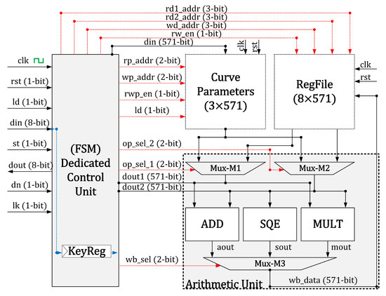
Figure 1.
Our large field-size elliptic curve cryptographic processor.

Table 1.
Description of the I/O pins and control signals of our proposed PM design.
3.1. Curve Parameters Unit
The objective of the curve parameter unit is to load the curve parameters and constants to implement the PM operation of ECC. Moreover, the flexibility in our architecture is achieved using the curve parameters unit. The flexibility means that the users can load different curve parameters and a scalar multiplier to our proposed processor for PM computation. The internal architecture of our curve parameter unit includes three 571-bit registers (i.e., , and b) to load the coordinate of initial point P and a curve constant value as the input from outside. Moreover, the output of the curve parameter unit depends on a multiplexer (not shown in Figure 1) to select an appropriate operand for the arithmetic unit as input. The corresponding values for , and b buffers are selected from the standardized NIST document [].
3.2. RegFile
It is essential to mention that the curve parameter and RegFile units are utilized for different purposes. Previously, we (already) described that the curve parameter unit loads the curve parameters and constant values for the Weierstrass model of ECC. These buffers never need to modify during the entire computation. Hence, these initial values can be used (at any time) during the entire PM execution. On the other hand, the objective of RegFile is to keep the initial, intermediate and final generated outputs. It means that the RegFile is mandated to update during the PM computation. Therefore, we used an size of a register array (RegFile). The internal design of the RegFile unit contains two sizes of multiplexers and one size of a demultiplexer. The multiplexers allow us to read two 571-bit operands from the register array and a demultiplexer updates the value of the specified register for writing back. For read/write operations, the related control signals are the responsibility of the control unit to generate.
3.3. Arithmetic Unit
An arithmetic unit is mandated to implement modular finite field operations such as addition, multiplication, square, reduction and inversion. As observed in Figure 1, the arithmetic unit consists of three routing multiplexers (M1, M2 and M3), an adder (ADD), a polynomial multiplier (MULT) and a square (SQE) unit. The design details of these circuit components are as follows.
Routing multiplexers (M1, M2 and M3). The routing multiplexers select the right operand for the modular arithmetic operators and RegFile block. The multiplexers M1 and M2 select an appropriate operand as the input to adder, multiplier and square units. The multiplexer M3 selects the outputs of these modular operators to be written back on the RegFile. The control unit generates the control signals to operate multiplexers M1, M2 and M3.
Modular addition (ADD). The realization of a modular adder over field is simple. It needs bitwise exclusive (OR) gates for implementations. Therefore, for two 571-bit operands, two-input 571 exclusives (OR) gates are needed [,,]. It takes one clock cycle for implementation.
Modular square (SQE). Like modular addition, the polynomial squaring in the binary field is relatively simple. Therefore, a 0-bit is required to place between two consecutive input data bits as explained in [,,,]. We also used this method to implement the modular square operation. It takes two 571-bit operands as input and results in a bit as output. Moreover, it bears one clock cycle for square implementation.
Proposed modular multiplier design. Before describing our proposed modular multiplier architecture, it is essential to provide the frequently utilized modular multiplication approaches in the literature. According to [], four different modular multiplication methods, i.e., (i) bit-serial, (ii) digit-serial, (iii) bit-parallel, and (iv) digit-parallel, are frequently adopted. Moreover, an open-source tool is described in [] to generate Verilog HDL implementations of different modular multipliers (schoolbook, Booth, 2-way Karatsuba, 3-way Toom-Cook and 4-way Toom-Cook). Moreover, their tool automatically generates the synthesis scripts to facilitate the ASIC designers. Therefore, the aforesaid multiplication techniques have their unique benefits and some disadvantages as well. The bit and digit serial methods are useful for implementing the area and power-optimized circuits [,]. For high-performance implementations, bit-parallel and digit-parallel multipliers are more useful [,,,]. The computational cost of these multiplication approaches is different. For example, for two l-bit sizes of polynomial operands to the multiplier as input, the bit-serial methods require cycles. The digit-serial approaches require cycles, where l is the operands length and m is the digit size. The computational cost of digit and bit-parallel approaches is a one clock cycle with area and power overheads. There is always a tradeoff between area, power and performance. We direct readers to [,] for more comprehensive comparisons over different multiplication architectures.
As shown in Figure 2, we have used a bit-parallel Karatsuba multiplier for modular multiplication computations. The cause of the implementation of the Karatsuba multiplier is to achieve a throughput/area-optimized circuit for PM computation. The one clock cycle requirement of Karatsuba for one polynomial multiplication allows us to reduce the overall clock cycles, which eventually increases the throughput. The hardware resources of the Karatsuba multiplier for square and inversion computation help to decrease the overall area requirement for the ECC point multiplication, which ensures that the proposed PM architecture is well-suited for the area-optimized applications. Karatsuba follows a divide-and-conquer approach for polynomial multiplications. For example, let us have two polynomials of length m-bit. To operate the Karatsuba multiplier, the polynomials length of m-bit needs to divide into two -bit smaller polynomials. Then, the Karatsuba multiplier operates on the smaller polynomials to generate the final polynomial. It is essential to note that the Karatsuba multiplier requires three inner multiplications (M1, M2 and M3 in Figure 2), some additions (A1, A2, A3 and A4 in Figure 2), and shift operations (S1 and S2 in Figure 2) for polynomial multiplications. Therefore, in our MULT block of Figure 1, the input polynomials of length 571 bits are partitioned into two pieces, i.e., 285, and 286. Then, the Karatsuba multiplier is applied on 285 and 286-bit polynomials to generate the resultant polynomial length of bits.
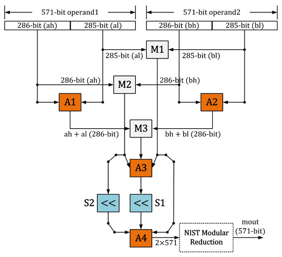
Figure 2.
Proposed Karatsuba modular multiplier.
As seen in Figure 2, three multipliers are required to implement the multiplications over 285 and 286-bit polynomial lengths. The M1 multiplies the 285-bits from the least-significant side of two input operands. Similarly, M2 multiplies the 286-bits from the most-significant side of two input operands. The M3 multiplies the sum of the least 285-bits and most 286-bits of two operands. Despite the inner multiplications, Karatsuba requires four modular additions. The adder (A1) adds the least 285-bit and most 286-bit of the first operand. Similarly, the A2 adds the least 285-bit and most 286-bit of the second operand. The adder A3 sums the multiplication result from M1 and M2. The last adder, i.e., A4, adds the sum of shifted polynomials to produce the resultant polynomial length of bits. The Karatsuba requires one clock cycle to implement one 571-bit polynomial multiplication.
NIST modular reduction. The modular square and multiplier result in a bit. Consequently, a modular reduction is mandated to operate to gain back our square and multiplier results in 571 bits. Several modular reduction approaches are available in the literature. Hence, we preferred to utilize modular reduction over recommended by NIST. We represented the modular reduction over in this work in Algorithm 2. Moreover, a block of Algorithm 2 is instantiated in our SQE and MULT units (not presented in Figure 1) to obtain the reduced polynomial in the same clock cycle. The reason is a combinational logic that we used to implement Algorithm 2 as it takes only shift and exclusive (OR) gates. Moreover, with the inclusion of the modular reduction computation, our SQE and MULT units take one clock cycle for implementation.
| Algorithm 2: NIST modular reduction over [] |
Input: Polynomial, with -bit length Output: Polynomial, with m-bit length
|
Modular inversion. As shown in Algorithm 1, the last two lines include a modular inversion computation. We have plenty of methods in the literature to perform the modular inversion. Not all inversion approaches are suitable to accelerate performances on hardware platforms due to the involvement of different mathematical structures []. Consequently, in our accelerator design, we have used a square version of an Itoh-Tsujii algorithm [] which requires squares equivalent to the field length followed by 12 modular multiplications over field. The modular inversion unit is not highlighted in Figure 1 because the beauty of the Itoh-Tsujii inversion algorithm is the square and multiplication requirements. Hence, the modular inversion operation is performed using the existing resources of the square and multiplication circuits as employed in PM architectures of [,,]. Thus, this approach reduces the hardware cost as well as the consumed power. As we described earlier in this work, the cost for one square and multiplier circuit is one clock cycle. Then, over , the implementation of the Itoh-Tsujii algorithm for modular inversion requires 571 clock cycles for square computations and 12 clock cycles for modular multiplication computation. The total cycle counts for one modular inversion computation is 583.
3.4. Control Unit and Clock Cycles Calculation
We employed an FSM-based dedicated controller to implement the Algorithm 1 for PM computation. For our implementations, we divide Algorithm 1 in four portions: (i) LSV, (ii) INT, (iii) PMC and (iv) GOP. The details are as follows. Moreover, FSM generates the corresponding control signals for the Curve Parameters unit, RegFile unit and the arithmetic unit.
- Loading secret vectors (LSV). A bit stream of a scalar multiplier k and coordinates of initial point P are required as input to Algorithm 1. Therefore, based on the related control signals, LSV determines the loading of ECC parameters and a scalar multiplier into the corresponding buffers (in the Curve Parameters unit). When a one-bit signal becomes 1, then it means that we have to load x and y coordinates of the initial point P and a curve constant b into the corresponding buffers of the Curve Parameters unit. The related control signals to our Curve Parameters unit are shown in Figure 1 and the related details are provided in Table 1. Similarly, when a one-bit signal becomes 1, it implies that we have to load a secret key (or a scalar multiplier k) into a KeyReg buffer, as shown in Figure 1. It is essential to provide that the interface of our processor architecture supports only 8-bit data loading using an 8-bit pin. Therefore, the 571-bit ECC parameters (i.e., , and b) and a secret key k needs to load in 8-bit form. For example, to load a 571-bit secret key in our KeyReg buffer, 72 clock cycles are required. Similarly, our design requires 3×72 clock cycles to load , and b in buffers of the Curve Parameters unit.
- Initialization (INT). Line one of Algorithm 1 specifies the initializations or conversions from affine to projective coordinates. As our implemented modular operators (adder, square and multiplier) require one clock cycle for one modular operation computation, 5 clock cycles are required for affine to projective conversions.
- Point multiplication computation (PMC). A for loop in Algorithm 1 defines the PM computation in Lopez Dahab projective coordinate system. The instructions mentioned in the if and else statements are for PA and PD operations. More precisely, from to are for PA and to are for PD. The switching between if and else statements relies on the value of the inspected one-bit scalar multiplier k. A total of fourteen instructions are concerned with PA and PD computations. Therefore, to implement the fourteen instructions, our design takes clock cycles, where m is the size of a secret key (i.e., 571).
- Generating output (GOP). Algorithm 1 produces x and y coordinates of a resultant point Q as an output. Therefore, the statements in the last two lines in Algorithm 1 are for generating the and coordinates of a final point Q. This stage is (also) known as reconversions from Lopez Dahab projective to affine coordinates. As observed in the last two lines of Algorithm 1, two modular inverse operations and some addition and multiplication operations are required to compute. As described earlier in this paper, our design requires 583 cycles for one inverse computation. So, we need 1166 clock cycles for two inverse operations. Moreover, our architecture takes 28 clock cycles for other addition and multiplication operations to compute. Hence, clock cycles are required for projective to affine conversions.
Consequently, the total clock cycles for one PM computation using Algorithm 1 over is 9165 (and can be calculated using cycles for + cycles for + cycles for ).
4. Results and Comparison
The implementation results and our comparison to the state-of-the-art are given in Section 4.1 and Section 4.2, respectively.
4.1. Results
Our large-field size design over is implemented in Verilog HDL using a Vivado IDE tool. We have selected the coordinates of the initial point P and a curve constant value b as inputs from NIST standardized document []. For Xilinx Virtex-6 and Virtex-7 FPGA devices, we have provided implementation results in Table 2 after place-and-route level. Columns one to three of Table 2 provide the hardware cost in slices, look-up-tables (LUTs) and flip-flops (FFs). The computation cost (of our proposed design) in terms of clock cycles, frequency (Freq in MHz), and latency (in s) are given in columns four to six. We have demonstrated the throughput values in column seven. We have computed a ratio of throughput over slices to show the performance of our proposed design and the calculated values are provided in the last column of Table 2. We have collected slices, LUTs, FFs and frequency values from the synthesis tool (i.e., Vivado IDE). We have already described the clock cycles calculation in Section 3.4. Moreover, we have calculated latency and throughput values from Equation (4) and Equation (5), respectively. Finally, we have calculated the throughput over area results using Equation (6). It is essential to mention that we have used slices as an area in Equation (6).
Table 2.
Implementation results of our large-field size ECC processor over on Xilinx FPGA devices.
Our proposed architecture on Xilinx Virtex-7 FPGA utilizes 1.07x (ratio of 6107 over 5683), 1.05x (ratio of 15,216 over 14,356) and 1.02x (ratio of 6103 over 5961) lower slices, LUTs and FFs as compared to Virtex-6 FPGA implementation. The cause of utilizing fewer resources on Virtex-7 devices is the difference in implementation technology because the Virtex-6 devices are constructed on a 40 nm process technology. On the other hand, the Virtex-7 devices are built on a 28 nm technology.
The clock cycle requirement of our design is 9165, as shown in column five of Table 2. It can be minimized using a quad Itoh-Tsujii inverse algorithm instead of a square version of the Itoh-Tsujii inversion algorithm (we used it in this work). Moreover, instruction level parallelism is another choice to decrease the clock cycle utilization of our design of Figure 1. With area overhead, multiple modular adders, multipliers, and square units can be used to reduce the clock cycles of our design. In addition, instructions rescheduling for PA and PD operations is another alternative to optimize the cycle count in ECC implementations. Comparing operational frequency, our architecture on Virtex-7 is 1.13x (ratio of 361 over 319) faster when compared to the Virtex-6 implementation. The pipeline registers in the circuit datapath are more practical to optimize the clock frequency and shorten the critical path. Digit-parallel multipliers are more convenient for minimizing the circuit delay when compared to the recursive multiplication approaches. We prefer a recursive modular multiplier (Karatsuba in this work) rather than a digit parallel because the digit-parallel multipliers utilize more hardware resources and the recursive multipliers result in longer circuit delay. There is always a tradeoff. As shown in column seven of Table 2, the time required to perform one PM computation on Virtex-7 is 25.38 s, which is comparatively 1.13x (ratio of 28.73 over 25.38) lower than the Virtex-6 implementation. The reason is the higher circuit frequency on the Virtex-7 device compared to the Virtex-6. The calculated value for throughput over the Virtex-7 device is 39.40 kbps, which is comparatively 1.13x (ratio of 39.40 over 34.80) higher than our Virtex-6 implementation (34.80kbps).
The higher the value for the performance metric, the higher will be the performance of the circuit/design. Therefore, as far as the performance metric is concerned for comparison, our design on Virtex-7 results in higher throughput over slices value (6.93), as shown in the last column of Table 2. The reason is the lower FPGA slice utilization and higher circuit frequency on the Virtex-7 device.
4.2. Comparisons
Table 3 provides the comparison to state-of-the-art PM designs on Xilinx Virtex-6 and Virtex-7 FPGA devices. Columns one and two of Table 3 provide the reference design (Ref. #) and the publication year, respectively. We have presented the implementation device in column three. The hardware resource utilizations in FPGA slices and LUTs are given in columns four and five. The clock cycle information is presented in column six. The achieved circuit frequency (in MHz) is shown in column seven. The latency (in s) and throughput () values are shown in columns eight and nine, respectively. Finally, the last two columns provide the throughput over area results. It is essential to mention that we have used ‘–’ in Table 3, where the relevant information is not reported in the reference-implemented design.
Table 3.
Comparison to most relevant state-of-the-art PM architectures over .
4.2.1. Comparison to Area, Clock Cycles, Latency, Frequency and Throughput
In this section, on different FPGA devices, we compared our implementation details in the area (slices and LUTs), clock cycles, computation time (i.e., latency), circuit frequency, and throughput with state-of-the-art implemented designs.
Comparison to Virtex-5 implementation: The comparison to [] reveals that our architecture is 1.59 (ratio of 11,640 over 7289) and 18.94 (ratio of 324,332 over 17,116) times more efficient in FPGA slices and LUTs. The reason is an additional polynomial inversion circuit using a digit serial variant of the Kim and Hong method in the reference design. In our implementation, we employed the Itoh-Tsujii inversion algorithm, which is implemented using the hardware resources of our square and multiplier circuits. Moreover, our PM implementation is 4.80 (ratio of 44,047 over 9165) and 2.33 (ratio of 296 over 127) times more efficient in clock cycles and circuit frequency, respectively. The cause is a digit serial multiplier in the reference design while we utilized a bit parallel Karatsuba multiplier for polynomial multiplications. Similarly, if we compare the latency and throughput values, our PM architecture is 11.24 (ratio of 348 over 30.96) and 11.25 (ratio of 32.29 over 2.87) times more efficient.
On an identical Virtex-5 device, our slices comparison to [] shows that the proposed accelerator architecture is 2.78 (ratio of 20,291 over 7289) times efficient. As shown in columns five to seven of Table 3, the comparison to LUTs, clock cycles and circuit frequency is not possible to make, as the corresponding information is not given in the reference design. In latency and throughput, the architecture of [] is 1.67 (ratio of 30.96 over 18.51) and 1.67 (ratio of 54.02 over 32.29) times more efficient as compared to our proposed accelerator architecture. In summary, we are winning the hardware resources, while the design of [] is more efficient in latency and throughput. There is always a tradeoff between area and throughput.
Comparison to Virtex-6 implementation: The comparison to [] shows that our architecture is 7.63 (ratio of 116,241 over 15,216) times more efficient in FPGA LUTs. As observed in column four of Table 3, the comparison to FPGA slices is not possible, as the corresponding information is not presented in the reference design. The reason for the use of higher FPGA LUTs in [] is that it is low latency ECC architecture with three modular multipliers in the datapath. In our implementation, we have only one modular multiplier. Furthermore, our PM architecture takes 9165 clock cycles for one PM computation while the reference design utilizes 7628 clock cycles (as given in column six of Table 3). The reason is three modular multipliers in the reference design (we used only one in our circuit). Our proposed design is 2.36 (ratio of 319 over 135) times more efficient in operating frequency. The reason is the shorter critical path as compared to the reference design. The comparison of latency and throughput shows that our PM architecture is 1.96 (ratio of 56.50 over 28.73) and 1.96 (ratio of 34.80 over 17.69) times more efficient.
Comparison to Virtex-7 implementation: Here, we are comparing only the hardware resources in slices and LUTs of our PM architecture to Virtex-7 implementations of [,,,]. As you can observe in columns four and five of Table 3, the value of the slices for [] and LUTs values for [] are not reported in the reference designs. Thus, our comparison to these implementations on these specific parameters (slices and LUTs) is not possible. However, the FPGA slices comparisons reveal that our PM architecture is 2.28 (ratio of 12,965 over 5683), 1.24 (ratio of 5683 over 4560) and 8.85 (ratio of 50,336 over 5683) times more efficient than [,,]. Similarly, the LUTs comparison shows that our PM implementation is 2.68 (ratio of 38,547 over 14,356), 1.13 (ratio of 14,356 over 12,691) and 5.64 (ratio of 80,970 over 14,356) times more efficient than [,,]. The reasons are different modular multipliers in the datapaths. For instance, in our PM design, we employed a recursive Karatsuba polynomial multiplication method, while in [], a digit parallel multiplier with a digit size of 41-bits is incorporated for PM implementation. Moreover, a 143-bit digit serial multiplier is employed in [] to implement modular multiplication over . Thus, different multipliers with different digit lengths result in different slices and LUTs and take different clock cycles for computation. There is always a tradeoff.
As shown in column six of Table 3, the comparison to clock cycles is not possible to [,], as the related information is not available in the reference designs. However, our PM design takes 1.34 (ratio of 12,329 over 9165) times lower clock cycles as compared to []. On the other hand, our implementation takes 9165 cycles, while the design of [] takes 3783 cycles. We know this happens due to three multipliers in the datapath of [], while we have only one modular multiplier in our PM implementation.
The comparison to circuit frequency reveals that our PM design is 1.31 (ratio of 361 over 274), 1.44 (ratio of 361 over 250), 1.06 (ratio of 361 over 340) and 3.25 (ratio of 361 over 111) times more efficient compared to [,,,]. Column eight in Table 3 shows that our proposed PM design requires lower computation time for one PM computation as compared to [,,]. However, on the other hand, the PM design of [] is more efficient in latency as compared to our proposed PM architecture. Similarly, column nine in Table 3 shows that the calculated values of throughput for our proposed PM design are higher compared to [,,]. But on the other hand, the PM design of [] is more efficient in throughput compared to our proposed PM architecture.
4.2.2. Comparison to Throughput/Area
In Section 4.2.1, the area and throughput comparison of our proposed PM architecture with state-of-the-art shows that our proposed PM design is more area and throughput efficient as compared to PM implementations of [,,,,,,]. In the throughput, the PM implementations of [,] are more efficient as compared to our work. Similarly, in the area, the PM architecture of [] is more efficient as compared to our proposed PM design. Therefore, to make a realistic comparison to the state-of-the-art, we have calculated throughput/area values using Equation (6). In Equation (6), we have used slices and LUTs as an area and the calculated values are (already) available in the last two columns of Table 3.
As compared to Xilinx Virtex-5 implementations of [], our PM design is 17.96 (ratio of 4.42 over 0.246) and 235 (ratio of 1.88 over 0.008) times more efficient in throughput/slices and throughput/LUTs. Our comparison to [] over throughput/LUTs is not possible, as the LUTs values are missing (as you can see in column five of Table 3). However, the throughput/slices comparison shows that our proposed architecture is 1.66 (ratio of 4.42 over 2.66) times more efficient.
If we compared our results to Xilinx Virtex-6 implementation of [], our PM design is 15.2 (ratio of 2.28 over 0.15) times more efficient in the throughput/LUTs. The comparison to throughput/slices is not possible as the slices values are not reported for the reference implemented design. For Virtex-7 FPGA implementations, the throughput/slices comparisons reveal that our PM architecture is 5.21 (ratio of 6.93 over 1.33), 1.14 (ratio of 6.93 over 6.04) and 11.94 (ratio of 6.93 over 0.58) times more efficient than [,,]. For the identical Virtex-7 devices, if we used LUTs as an area instead of slices in Equation (6), the throughput/LUTs comparison shows that our PM implementation is 6.08 (ratio of 2.74 over 0.45), 1.26 (ratio of 2.74 over 2.17) and 2.79 (ratio of 2.74 over 0.98) times more efficient than [,,].
In a nutshell, on different Xilinx FPGA devices (Virtex-5, Virtex-6 and Virtex-7), the last two columns of Table 3 reveals that the proposed PM architecture outperforms in throughput/slices and throughput/LUTs values as compared to the most recent state-of-the-art PM-implemented designs.
5. Conclusions and Future Trends
A flexible throughput/area ECC processor is presented over for PM computation on Xilinx Virtex-6 and Virtex-7 FPGA devices. This study demonstrates that the Lopez-Dahab projective coordinates help to decrease the total clock cycles. Moreover, a fully recursive Karatsuba multiplier is beneficial to minimize the cycle counts for the PM computation of the ECC. Furthermore, the use of a modular multiplier to implement the modular square and inversion operations of ECC is appropriate to save hardware resources. Based on the aforesaid observations, the comparison to existing PM designs in the literature shows that the proposed architecture outperforms in throughput/area and is suitable for applications that require throughput and area simultaneously for implementation.
The performance, in terms of the hardware area, of the proposed PM architecture, could be improved by employing bit- and digit-serial multiplication approaches with the throughput overhead. The throughput of the proposed architecture is possible to optimize by the rescheduling of PA and PD instructions for PM computation. For high-speed cryptographic applications, multiple adders and Karatsuba multipliers can be instantiated in the datapath of the PM design to optimize the circuit frequency and reduce clock cycles. These strategies help to reduce the computation time for one PM operation.
Author Contributions
Conceptualization, S.S.J. and A.A. (Ahmed Alhomoud) and A.A. (Amer Aljaedi); methodology, A.A. (Ahmed Alhomoud) and A.R.A.; software, A.A. (Amer Aljaedi); validation, S.S.J. and A.R.A. and A.A. (Ahmed Alhomoud); formal analysis, A.A. (Ahmed Alhomoud) and A.A. (Amer Aljaedi); investigation, S.S.J. and A.A. (Ahmed Alhomoud); resources, A.A. (Ahmed Alhomoud) and A.A. (Amer Aljaedi) and S.S.J. and S.M.A. and M.A.; data curation, A.A. (Ahmed Alhomoud); writing—original draft preparation, S.S.J. and A.A. (Amer Aljaedi); writing—review and editing, S.S.J. and S.M.A. and M.A.; visualization, S.S.J.; supervision, S.S.J. and A.A. (Ahmed Alhomoud). All authors have read and agreed to the published version of the manuscript.
Funding
This work is funded by the Deanship of Scientific Research at Northern Border University, Arar, Kingdom of Saudi Arabia under grant number RG-NBU-2022-11-1936.
Institutional Review Board Statement
Not applicable.
Informed Consent Statement
Not applicable.
Data Availability Statement
Not applicable.
Acknowledgments
The authors gratefully acknowledge the approval and the support of this research study by the grant no. RG-NBU-2022-11-1936 from the Deanship of Scientific Research at Northern Border University, Arar, Kingdom of Saudi Arabia.
Conflicts of Interest
The authors declare no conflict of interest.
References
- Miller, V.S. Use of Elliptic Curves in Cryptography. In Proceedings of the Advances in Cryptology—CRYPTO ’85 Proceedings; Williams, H.C., Ed.; Springer: Berlin/Heidelberg, Germany, 1986; pp. 417–426. [Google Scholar]
- Rivest, R.L.; Shamir, A.; Adleman, L. A method for obtaining digital signatures and public-key cryptosystems. Commun. ACM 1978, 21, 120–126. [Google Scholar] [CrossRef]
- Kumar, K.A.; Krishna, A.V.N.; Chatrapati, K.S. New secure routing protocol with elliptic curve cryptography for military heterogeneous wireless sensor networks. J. Inf. Optim. Sci. 2017, 38, 341–365. [Google Scholar] [CrossRef]
- Gulen, U.; Baktir, S. Elliptic Curve Cryptography for Wireless Sensor Networks Using the Number Theoretic Transform. Sensors 2020, 20, 1507. [Google Scholar] [CrossRef] [PubMed]
- Noori, D.; Shakeri, H.; Niazi, T.M. Scalable, efficient, and secure RFID with elliptic curve cryptosystem for Internet of Things in healthcare environment. EURASIP J. Inf. Secur. 2020, 2020, 13. [Google Scholar] [CrossRef]
- Calderoni, L.; Maio, D. Lightweight Security Settings in RFID Technology for Smart Agri-Food Certification. In Proceedings of the 2020 IEEE International Conference on Smart Computing (SMARTCOMP), Bologna, Italy, 14–17 September 2020; pp. 226–231. [Google Scholar] [CrossRef]
- Singh, R.; Miglani, S. Efficient and secure message transfer in VANET. In Proceedings of the 2016 International Conference on Inventive Computation Technologies (ICICT), Coimbatore, India, 26–27 August 2016; Volume 2, pp. 1–5. [Google Scholar] [CrossRef]
- Chavhan, S.; Doriya, R. Secured Map Building using Elliptic Curve Integrated Encryption Scheme and Kerberos for Cloud-based Robots. In Proceedings of the 2020 Fourth International Conference on Computing Methodologies and Communication (ICCMC), Erode, India, 11–13 March 2020; pp. 157–164. [Google Scholar] [CrossRef]
- NIST. Recommended Elliptic Curves for Federal Government Use. 1999. Available online: https://csrc.nist.gov/csrc/media/publications/fips/186/2/archive/2000-01-27/documents/fips186-2.pdf (accessed on 28 October 2022).
- Hankerson, D.; Menezes, A.J.; Vanstone, S. Guide to Elliptic Curve Cryptography; 2004; pp. 1–311. Available online: https://link.springer.com/book/10.1007/b97644 (accessed on 7 November 2022).
- Rashid, M.; Imran, M.; Jafri, A.R.; Al-Somani, T.F. Flexible Architectures for Cryptographic Algorithms — A Systematic Literature Review. J. Circuits Syst. Comput. 2019, 28, 1930003. [Google Scholar] [CrossRef]
- Imran, M.; Rashid, M.; Jafri, A.R.; Kashif, M. Throughput/area optimised pipelined architecture for elliptic curve crypto processor. IET Comput. Digit. Tech. 2019, 13, 361–368. [Google Scholar] [CrossRef]
- Islam, M.M.; Hossain, M.S.; Hasan, M.K.; Shahjalal, M.; Jang, Y. FPGA Implementation of High-Speed Area-Efficient Processor for Elliptic Curve Point Multiplication Over Prime Field. IEEE Access 2019, 7, 178811–178826. [Google Scholar] [CrossRef]
- Rashid, M.; Imran, M.; Kashif, M.; Sajid, A. An Optimized Architecture for Binary Huff Curves With Improved Security. IEEE Access 2021, 9, 88498–88511. [Google Scholar] [CrossRef]
- Khan, Z.U.A.; Benaissa, M. Throughput/Area-efficient ECC Processor Using Montgomery Point Multiplication on FPGA. IEEE Trans. Circuits Syst. II Express Briefs 2015, 62, 1078–1082. [Google Scholar] [CrossRef]
- Imran, M.; Pagliarini, S.; Rashid, M. An Area Aware Accelerator for Elliptic Curve Point Multiplication. In Proceedings of the 2020 27th IEEE International Conference on Electronics, Circuits and Systems (ICECS), Glasgow, UK, 23–25 November 2020; pp. 1–4. [Google Scholar] [CrossRef]
- Li, L.; Li, S. High-Performance Pipelined Architecture of Point Multiplication on Koblitz Curves. IEEE Trans. Circuits Syst. II Express Briefs 2018, 65, 1723–1727. [Google Scholar] [CrossRef]
- Li, J.; Wang, W.; Zhang, J.; Luo, Y.; Ren, S. Innovative Dual-Binary-Field Architecture for Point Multiplication of Elliptic Curve Cryptography. IEEE Access 2021, 9, 12405–12419. [Google Scholar] [CrossRef]
- Zhao, X.; Li, B.; Zhang, L.; Wang, Y.; Zhang, Y.; Chen, R. FPGA Implementation of High-Efficiency ECC Point Multiplication Circuit. Electronics 2021, 10, 1252. [Google Scholar] [CrossRef]
- Sutter, G.D.; Deschamps, J.P.; Imana, J.L. Efficient Elliptic Curve Point Multiplication Using Digit-Serial Binary Field Operations. IEEE Trans. Ind. Electron. 2013, 60, 217–225. [Google Scholar] [CrossRef]
- Khan, Z.U.A.; Benaissa, M. High-Speed and Low-Latency ECC Processor Implementation Over GF( 2m) on FPGA. IEEE Trans. Very Large Scale Integr. Syst. 2017, 25, 165–176. [Google Scholar] [CrossRef]
- Itoh, T.; Tsujii, S. A fast algorithm for computing multiplicative inverses in GF (2m) using normal bases. Inf. Comput. 1988, 78, 171–177. [Google Scholar] [CrossRef]
- Rashid, M.; Imran, M.; Jafri, A.R.; Mehmood, Z. A 4-Stage Pipelined Architecture for Point Multiplication of Binary Huff Curves. J. Circuits Syst. Comput. 2020, 29, 2050179. [Google Scholar] [CrossRef]
- Islam, M.M.; Hossain, M.S.; Hasan, M.K.; Shahjalal, M.; Jang, Y.M. Design and Implementation of High-Performance ECC Processor with Unified Point Addition on Twisted Edwards Curve. Sensors 2020, 20, 5148. [Google Scholar] [CrossRef]
- Lara-Nino, C.A.; Diaz-Perez, A.; Morales-Sandoval, M. Lightweight elliptic curve cryptography accelerator for internet of things applications. Ad Hoc Netw. 2020, 103, 102159. [Google Scholar] [CrossRef]
- Sajid, A.; Rashid, M.; Imran, M.; Jafri, A.R. A Low-Complexity Edward-Curve Point Multiplication Architecture. Electronics 2021, 10, 1080. [Google Scholar] [CrossRef]
- Imran, M.; Rashid, M. Architectural review of polynomial bases finite field multipliers over GF(2m). In Proceedings of the 2017 International Conference on Communication, Computing and Digital Systems (C-CODE), Islamabad, Pakistan, 8–9 March 2017; pp. 331–336. [Google Scholar] [CrossRef]
- Imran, M.; Abideen, Z.U.; Pagliarini, S. An Open-source Library of Large Integer Polynomial Multipliers. In Proceedings of the 2021 24th International Symposium on Design and Diagnostics of Electronic Circuits & Systems (DDECS), Vienna, Austria, 7–9 April 2021; pp. 145–150. [Google Scholar] [CrossRef]
Disclaimer/Publisher’s Note: The statements, opinions and data contained in all publications are solely those of the individual author(s) and contributor(s) and not of MDPI and/or the editor(s). MDPI and/or the editor(s) disclaim responsibility for any injury to people or property resulting from any ideas, methods, instructions or products referred to in the content. |
© 2023 by the authors. Licensee MDPI, Basel, Switzerland. This article is an open access article distributed under the terms and conditions of the Creative Commons Attribution (CC BY) license (https://creativecommons.org/licenses/by/4.0/).