1. Introduction
Our world is characterized by the widespread distribution of various cyber-physical systems (CPSs) into all spheres of human activity [
1,
2,
3]. Currently, intensive research is being carried out in the field of designing and ensuring the safety of the operation of CPSs [
4,
5,
6,
7,
8,
9]. As the name suggests, these systems include digital (cybernetic) parts interacting with physical objects [
10,
11,
12]. Very often, these digital parts include various sequential blocks [
3,
11]. These blocks can implement, for example, various security algorithms [
13]. To improve the overall quality of a cybernetic part, it is necessary to optimize characteristics of its sequential blocks. In the current paper, we discuss a case where the sequential blocks of digital parts are represented by finite state machines (FSMs) [
14].
Very often, the models of Mealy FSMs are used for the specification of sequential blocks [
14,
15]. The process of FSM design requires balancing the values of the occupied chip area, the maximum operating frequency, and power consumption [
16,
17]. We discuss a case where FSM circuits are designed with field-programmable gate arrays (FPGAs). The look-up table (LUT) elements are the basic elements used for implementing FSM circuits. As follows from [
18,
19], the circuit area has the greatest influence on the values of other characteristics. The area can be reduced due to jointly applying various methods of structural decomposition. In our paper [
20], we propose an optimization method based on jointly applying the methods of twofold state assignment (TSA) and encoding of output collections. As a result, LUT-based FSM circuits have exactly three logic levels. Let us point out that FPGAs are very popular in modern digital systems design [
5,
7,
8].
In this paper, we focus our attention on FPGA chips produced by AMD Xilinx [
21] because this corporation is the largest manufacturer of FPGA chips. To implement an FSM circuit, we use configurable logic blocks (CLBs) that include four main components: LUTs, programmable flip-flops, dedicated multiplexers, and fast interconnections. To obtain a multi-CLB circuit, the system of inter-CLB programmable interconnects should be used. The proposed method reduces the values of LUT counts in the multi-level circuits of Mealy FSMs.
The main principle of TSA-based FSMs assumes using two types of internal state codes [
20]. Each state is represented by both a maximum binary state code (MBC) and an extended state code (ESC) [
20]. Such an approach allows for reducing FSM hardware compared to methods based solely on MBCs. However, the approach in [
20] is connected with some overhead. Namely, an additional state transformer block should convert MBCs into ESCs. This converter consumes additional LUTs and interconnections. In this paper, we show how to reduce the noted overhead.
The main contribution of this paper boils down to the following. We have proposed: (1) a novel design method aimed at reducing the LUT counts in the circuits of FPGA-based Mealy FSMs with twofold state assignment and encoding of output collections; (2) a generalized FSM architecture, including three blocks of partial Boolean functions (PBFs); (3) a method of choosing one of seven possible FSM architectures based on the generalized architecture. To reduce hardware, we propose to use at least two cores of logic [
22]. The first core generates PBFs based on MBCs. The second core uses ESCs for this purpose. This approach allows for reducing hardware in the state transformer circuit because now only a part of the MBCs is transformed into ESCs. The scientific novelty of the proposed approach also includes an improvement in the known method of encoding of output collections by some additional variables. This encoding is done so that each of the cores includes some additional variables that do not occur in the second core. Thanks to this approach, the number of LUTs generating additional variables is reduced. Our current research shows that joint usage of these two approaches leads to FSM circuits having fewer LUTs compared to FSM circuits based on the approach in [
20]. The experimental results show that the proposed approach does not lead to significant deterioration of FSM temporal characteristics.
The remainder of the article is organized as follows.
Section 2 presents the background of FPGA-based Mealy FSM design.
Section 3 includes an analysis of relevant works.
Section 4 is devoted to representing a main idea of the proposed method. An example of FSM synthesis is discussed in
Section 5. The conducted experiments are analyzed in
Section 6. A generalized FSM architecture is discussed in
Section 7. Finally,
Section 8 is a short conclusion that summarizes the results.
2. Background Information for FPGA-Based Mealy FSMs
A Mealy FSM has M internal states, L external inputs, and N outputs used by other blocks of a CPS. To organize interstate transitions, special internal objects are used. These include R1 state variables and R1 input memory functions (IMFs). These objects are combined into corresponding sets
S,
I,
O,
SV, and
D [
14], which represent the following:
,
,
,
, and
. The sets
S,
I, and
O uniquely follow from, for example, the FSM state transition graph (STG) [
23]. However, the value of the parameter R1 is chosen by the circuit designer during the state assignment stage [
23].
In the case of MBCs [
24], the following formula determines the value of R1:
Formula (
1) determines the number of bits for MBCs (this is the minimum possible number for the given number of states). In the case of one-hot state assignment [
24], the value of R1 is equal to the number of states (
).
The state variables
create so-called full state codes
. Each state code bit corresponds to a flip-flop from a register
RG. The register is controlled by IMFs and two special pulses,
Res and
Clk [
25]. The pulse
Res executes the initialization of the FSM operation. This pulse sets an FSM in the initial state
. The pulse
Clk determines the instant of state code loading into RG. The
r-th bit of
is determined by the value of
. Like the vast majority of researchers, we use D flip-flops to organize the register RG [
26].
The following internal resources of FPGA fabric are involved in implementing an FSM circuit: LUTs, flip-flops, programmable interconnections, a synchronization tree, and programmable input–outputs [
27,
28]. In this paper, we consider a case where FPGAs of AMD Xilinx [
25] are used.
A LUT is a functional generator having
inputs and a single output [
24,
29]. A LUT may keep a truth table of any Boolean function it depends on up to
Boolean arguments. Nowadays, the value of
does not exceed 6. However, using dedicated multiplexers, the number of inputs can be increased to 8 (within a single CLB) [
27]. If the number of Boolean arguments exceeds 8, then a corresponding function is represented by a multi-CLB circuit. This leads to the necessity of minimizing the number of LUTs and their levels in the resulting circuit [
30,
31]. In this paper, we denote by the symbol
LUTer a block consisting of LUTs, multiplexers, flip-flops, and interconnections. All these elements are programmable [
32].
Two systems of Boolean functions (SBFs) represent an FSM logic circuit. They are the following [
17]:
These SBFs define a so-called
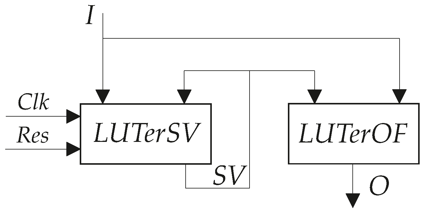
P Mealy FSM whose architecture is shown in
Figure 1 [
14].
In
Figure 1, the block
LUTerSV implements IMFs (
2). The IMFs determine the next state code (a code of the state of transition). The flip-flops of register RG are distributed among the elements of
LUTerSV. The pulses
Clk and
Res control the operation of flip-flops. The block LUTerOF generates output functions (
3).
The analysis of SBFs (
2) and (
3) shows that their functions depend on variables
and
. Each function
depends on
state variables and
inputs. The number of LUT levels in the corresponding circuit depends on the following condition:
If (
4) holds, then there is a single LUT in the corresponding logic circuit. The FSM circuit is single-level if condition (
4) holds for each function belonging to SBFs (
2) and (
3). In this case, the resulting FSM circuit is characterized by the best possible values of its main characteristics. This means that this circuit requires the minimum possible chip area, that it consumes the minimum possible power, and that it represents the fastest possible solution.
Even average FSMs can have up to 10 state variables and 30 inputs [
14]. Therefore, each function belonging to (
2) and (
3) may have up to 40 arguments. However, the number of LUT inputs is extremely small (
). In this regard, the probability of violation of the condition (
4) is very high. In the case of violation, various optimization methods are used to improve the characteristics of an FSM circuit. In this paper, we discuss a case where condition (
4) is violated.
3. Analysis of Related Work
Methods for improving spatial characteristics of FSM circuits are discussed in thousands of scientific works. For example, they can be found in [
18,
19,
25,
30,
32,
33,
34,
35,
36,
37,
38]. To estimate the chip area required for a LUT-based circuit, the designers use the values of LUT counts [
18]. Therefore, reducing the value of LUT count leads to a decrease in the area occupied by the circuit. This goal can be achieved using: 1. an optimal state assignment; 2. a functional decomposition (FD) of SBFs (
2) and (
3); and 3. a structural decomposition (SD) of the FSM logic circuit [
19].
The optimal state assignment excludes some literals from sum-of-products (SOPs) of functions (
2) and (
3) [
39]. In the best case, this exclusion allows for implementing a single-level Mealy FSM circuit. One of best state assignment methods is JEDI, which is distributed together with the CAD tool SIS [
40]. In the work of [
41], results of applying JEDI to FSMs from the library LGSynth93 are shown [
42]. These results show that JEDI allows for excluding up to 3 literals from SOPs (
2) and (
3), representing the benchmark FSMs. Therefore, using JEDI can turn multi-level circuits into single-level ones only for rather simple FSMs [
32].
Using either FD or SD leads to representing SBFs (
2) and (
3) by systems of partial Boolean functions [
34,
43]. Each PBF should depend on no more than
arguments. In this case, each PBF will be represented by a single-LUT circuit. Applying any type of decomposition produces multi-level FSM circuits. However, there is a fundamental difference in the resulting interconnection system for different decomposition methods [
19]. Applying the functional decomposition leads to FSM circuits with a “spaghetti-type” irregular interconnect system. In such a system, the same inputs and state variables may appear at any place on the circuit. Let us point out that the system of interconnections has a regular character for SD-based FSM circuits. An SD-based FSM circuit consists of large blocks [
19]. Each block has its unique systems of input variables and output functions, which can differ from FSM inputs
and state variables
. Due to this, SD-based circuits have better quality than the equivalent FD-based circuits [
19].
One such method is the encoding of FSM output collections (OCs) [
19]. A collection
is a set of outputs
that are generated simultaneously during the same interstate transition. If a particular STG has
H interstate transitions, then the number of OCs,
Q, differs from 1 to H [
19].
To encode
Q OCs by maximum binary codes
, R2 variables are enough:
These variables create the set
. There are two SBFs representing the system of FSM outputs [
19]:
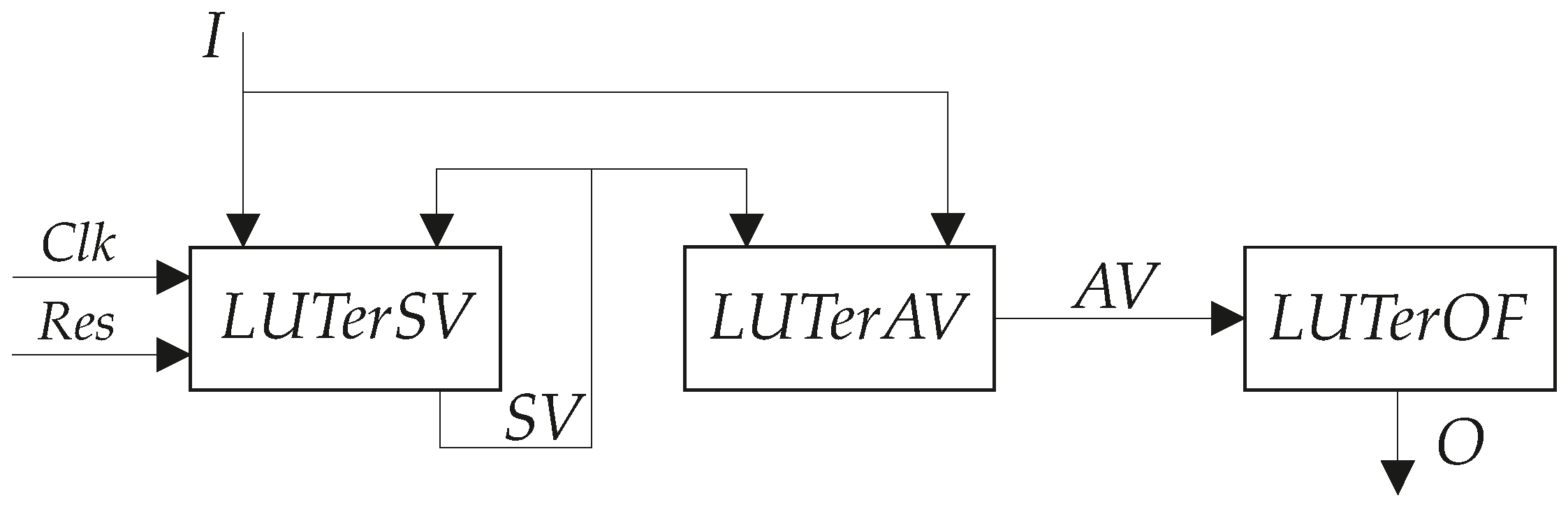
Applying this approach turns
P Mealy FSM into
PY Mealy FSM (
Figure 2).
In the LUT-based
PY Mealy FSM, the block
LUTerSV implements SBF (
2). The block
LUTerAV generates the additional variables represented by SBF (
6). The block
LUTerOF produces the FSM outputs represented by SBF (
7).
As follows from the research [
44], this approach allows for reducing the chip area necessary for generating FSM outputs compared to this parameter if the outputs are represented by SBF (
3). However, this gain reduces the value of the maximum operating frequency compared to an equivalent
P Mealy FSM. To optimize characteristics of
PY Mealy FSMs, the encoding of OCs may be connected with a twofold state assignment [
20], leading to
Mealy FSMs. We will discuss them a bit further.
To execute the TSA, we should find a partition of the set S by K classes. Each class includes compatible states. States , are compatible if their inclusion in the same class of the partition does not lead to the following phenomenon: the required number of LUT inputs exceeds the maximum number of inputs of LUT . Why such a phenomenon is possible will be clear from the further text of the article. Three sets characterize any class . These sets consist of: 1. inputs determining transitions from states (a set including elements); 2. outputs produced during the transitions from these states (a set ); and 3. IMFs determining MBCs of transition states (a set ). If the encoding of OCs is used, then the set is replaced by set . The set includes additional variables equal to 1 in the codes of OCs generated during the transitions from states .
Each class
includes
compatible states
. Inside each class, the states are encoded by partial codes
. These codes have
bits:
To create the partial codes, a set ASV of additional state variables is created. The states
are encoded using the variables
. The sets
create the set ASV, which includes R3 elements:
If a state
is compatible with states
, then including this state into
satisfies the condition:
This approach leads to a Mealy FSM. In Mealy FSMs, each state has two codes. One of them is a maximum binary full state code , and the second is a partial state code . The second code determines a particular state as an element of a particular class.
Each class
determines the following two systems of PBFs:
To obtain the final values of additional variables and IMFs, the following SBFs should be created:
Next, the codes of the OCs should be transformed into FSM outputs. The outputs are represented by SBF (
7). Additionally, the full state codes should be transformed into the corresponding partial codes. The transformation is represented by the following SBF:
SBFs (
11) and (
12) define the first level of a
Mealy FSM circuit. SBFs (
13) and (
14) determine its second level. Finally, SBFs (
7) and (
15) represent the third circuit level. The architecture of a
Mealy FSM is shown in
Figure 3.
In this architecture, the block
LUTerk generates PBFs (
11) and (
12). The block
LUTerPF implements the system of disjunctions (
13) and (
14). This block includes the distributed RG controlled by the pulses
Clk and
Res. The block
LUTerOF implements the outputs represented by SBF (
7). The block LUTerASV implements SBF (
15). Therefore, it executes the transformation of state codes.
Our previous research [
20] shows that the LUT-based circuits of
FSMs have better characteristics than the circuits of equivalent
PY FSMs. If the conditions
hold, then the circuits of
FSMs are three-level and are faster than the equivalent
PY Mealy FSMs.
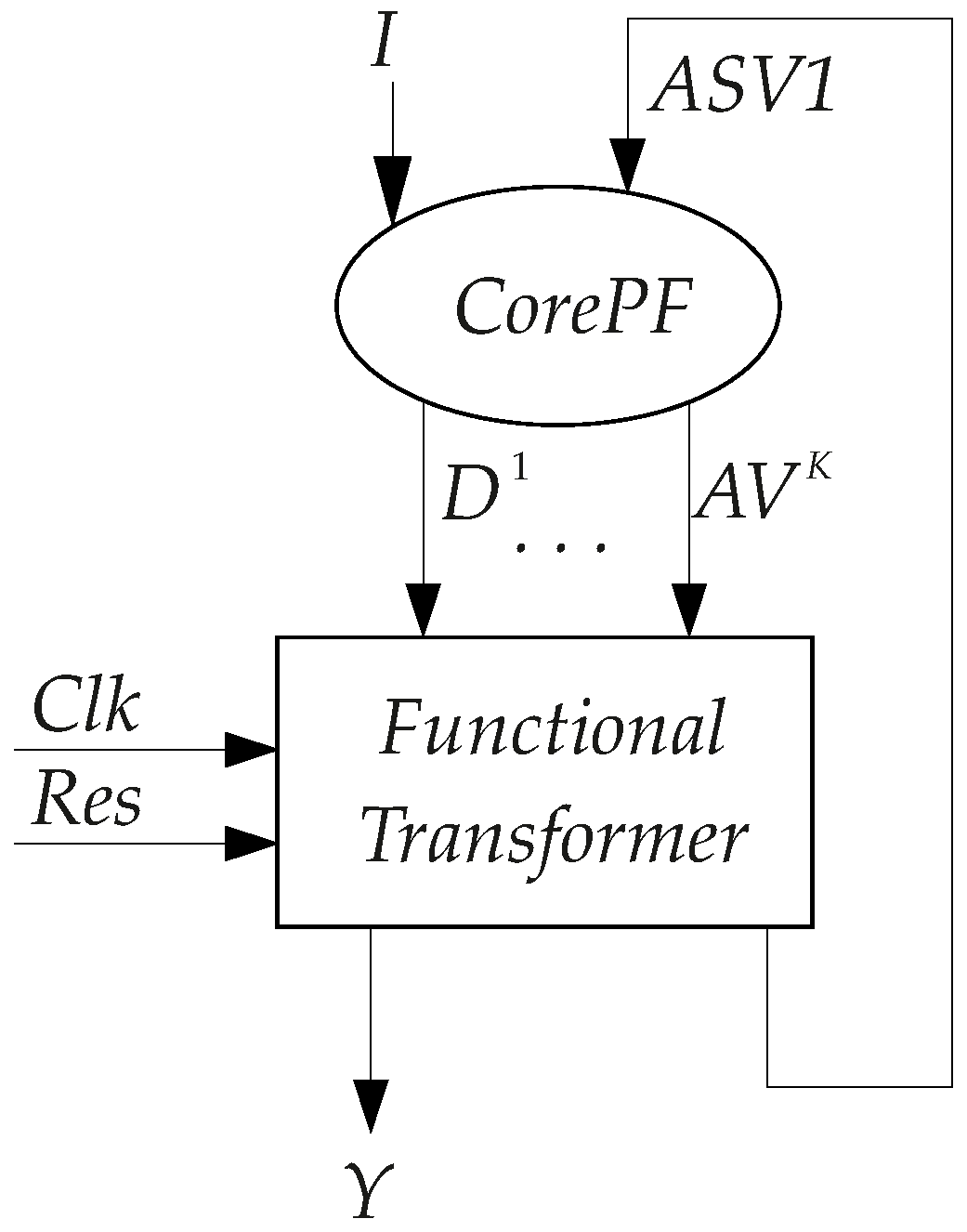
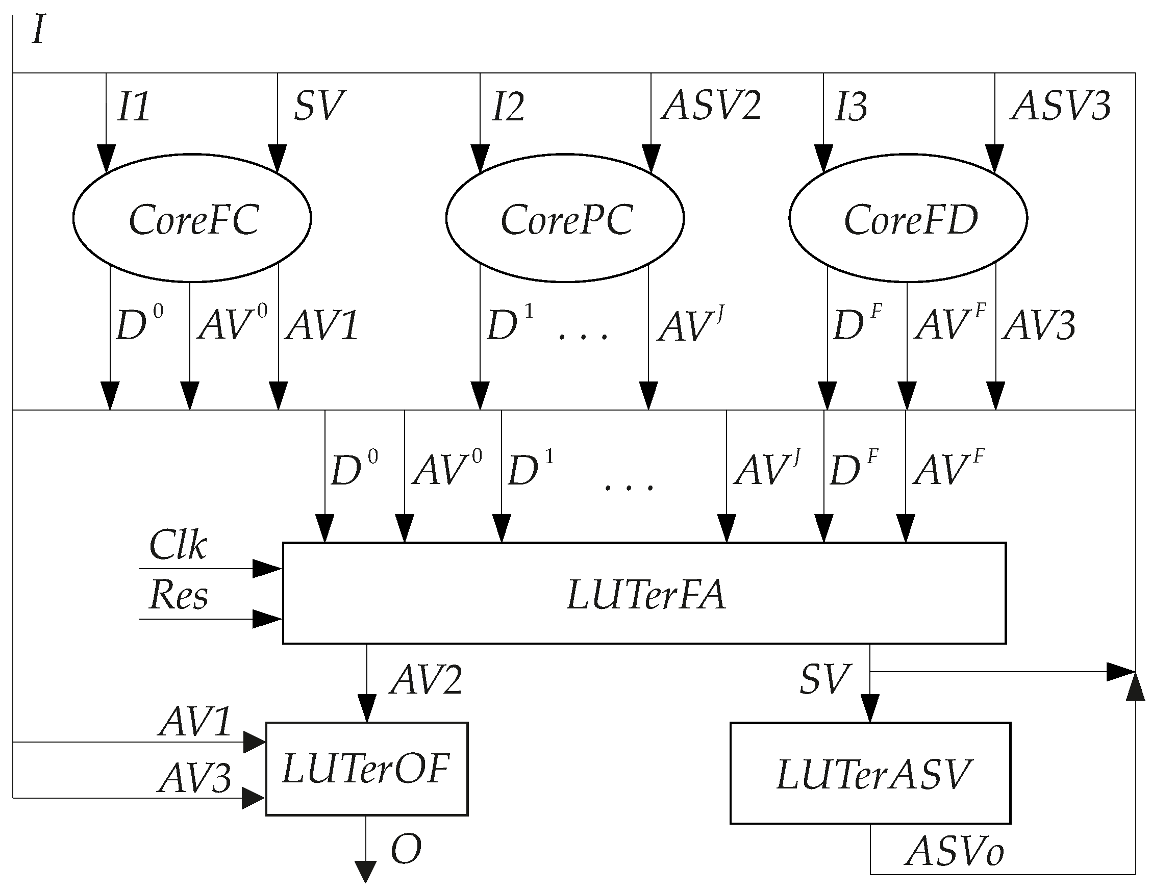
Let us represent the circuit (
Figure 3) as a combination of a core of partial functions (
CorePF) and a functional transformer. The core includes blocks
LUTer1–
LUTerK. The functional transformer includes all other blocks shown in
Figure 3. This leads to the generalized diagram of a
FSM (
Figure 4).
Analysis of the generalized diagram shows the following peculiarity: the transformation of full codes into partial codes
is executed for all FSM states. However, there is a case when there is no need in the code transformation. If, for some state
, condition (
4) holds, then, for this state, all PBFs are represented by single-LUT circuits. If we take into account this property, we can reduce the cardinality number of the partition
. Additionally, the number of state variables R3 can be reduced as compared to its value for the equivalent
FSM. In this paper, we propose a method based on taking into account the mentioned property.
4. Analysis of Our Current Approach
The transitions from state
are determined by elements of a set
. There are
elements in the set
. If the condition
holds, then it is enough for a single LUT to represent a circuit for any PBF generated during the transitions from
. Therefore, for such states, it makes sense to use the full state codes for generating PBFs. If the condition (
18) is violated, then the corresponding codes
should be transformed into partial codes. This allows for creating a class of states
whose maximum binary codes do not require the transformation. Therefore, the partition based on (
10) should be constructed only for the states
.
Based on the above-mentioned statement, we propose to use the ideas from our paper [
22]. First of all, we should divide the set
S by disjoint sets
and
. If a state
satisfies condition (
18), then this state is included in the set
. The states
create a block
CoreFC. Otherwise, the state
belongs to the set
S1. The states
form a block
CorePC. Obviously, only the codes of states
should be transformed.
CoreFC determines the sets
,
, and
. The input
causes the transitions from states creating the
CoreFC. The set
AV1 consists of additional variables
produced only during the transitions from states creating the
CoreFC. The set
consists of the additional variables produced by both FSM cores. The set
includes functions
produced during the transitions creating the
CoreFC. Therefore, the circuit of
CoreFC is determined by the following SBFs:
To synthesize CorePC, it is necessary to create the partition of the set S1. This can be done using the same approach as the one creating . CorePC determines the sets and . Their purpose is clear from the previous analysis.
Three sets (
,
,
) are determined by each class
of the partition
. Their meaning follows from the previous text. The state variables from the set
ASV2 encode the states
. The codes of states
are created from elements of the set
. There are
R4 elements in the set
. The following SBFs determine the circuit of
CorePC:
To generate the final values of additional variables, FSM outputs, and state variables, we should use the functional transformer. This block is similar to the one used in the
FSM (
Figure 3). Using this information, we propose to transform
FSMs into
Mealy FSMs (
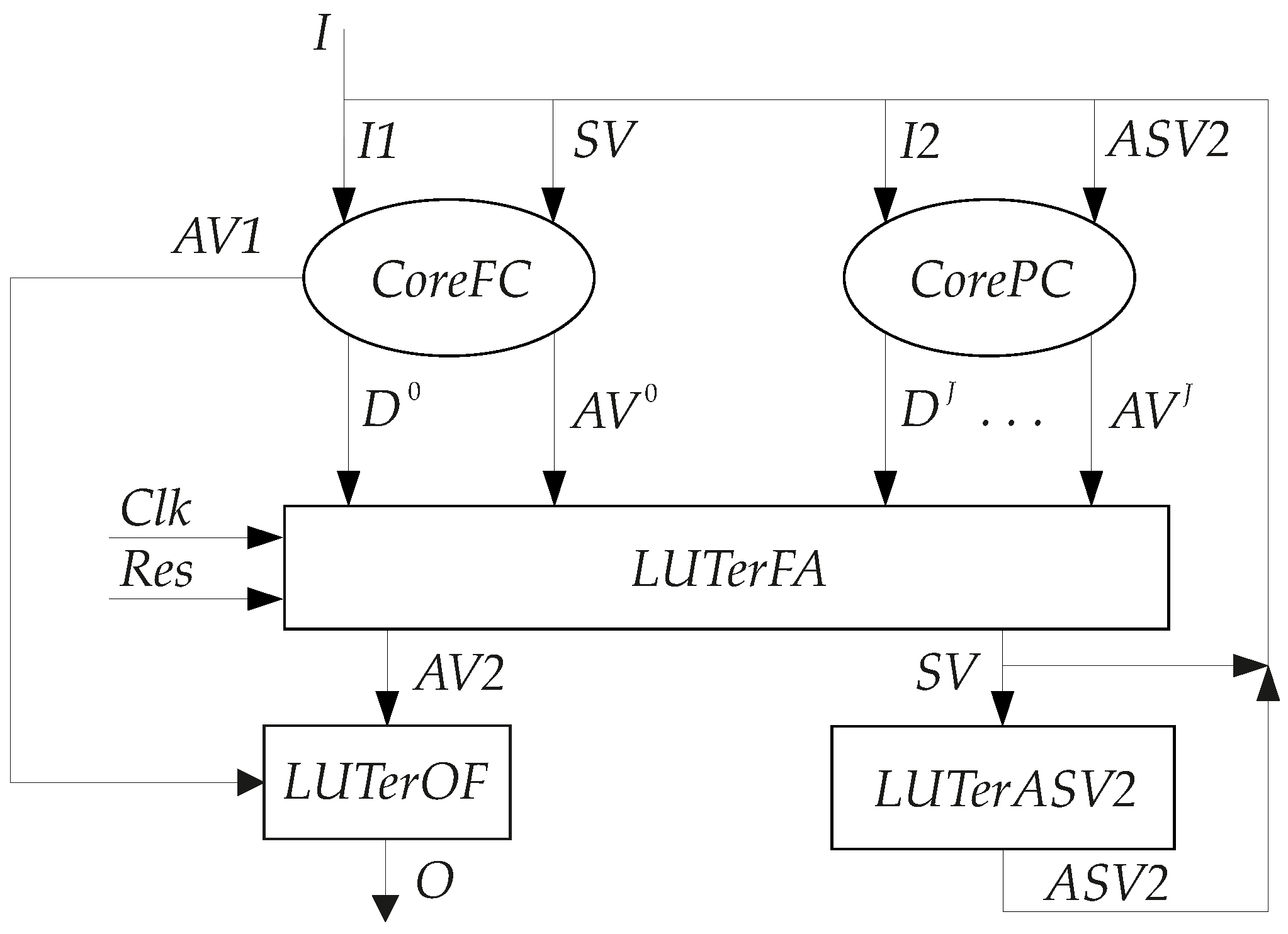
Figure 5).
In the proposed two-core FSM, the block
CoreFC implements SBFs (
19)–(
21). The block
CorePC implements SBFs (
22) and (
23). The block
LUTerFA is a functional assembler implementing the following disjunctions:
The block
LUTerFA includes a distributed full state code register whose informational inputs are connected with IMFs (
24). The register is controlled by pulses
Clk and
Res. The block
LUTerOF implements SBF (
7) where
. The block
LUTerASV2 implements SBF:
Let us analyze the proposed solution. The partition
has
J classes. Obviously, the following conditions take place:
Due to the validity of condition (
27), we can state that the circuit of the
Mealy FSM (
Figure 5) is not slower than the circuit of the equivalent FSM
(
Figure 3). Due to the validity of condition (
28), we can state that the circuit of
CorePC for FSM
should perform better LUT counts than it does for block
CorePF of the equivalent FSM
. The same is true for block
LUTerASV of the equivalent FSMs
and
. Therefore, we could expect that a circuit of
FSM (
Figure 5) requires a smaller area and is not slower compared to a circuit of equivalent
FSM (
Figure 3). These assumptions of ours have been confirmed by the conducted studies, the results of which are given in
Section 6.
Let us show the features of our method in comparison with the methods proposed in [
20,
22]. In the article [
20], we discussed
FSMs with two-fold state assignment and encoding of output collections. The
FSMs have the following differences. First, in
FSMs, the codes of all states are converted, while in
FSMs, only a part of the code is converted. This allows for optimizing the code converter circuit (compared to the circuit used in equivalent
FSMs). Secondly, the use of two cores allows us to encode OCs such that some variables
are generated only by the LUTs of
CoreFC. This allows for reducing the number of LUTs generating output signals (compared to this number for equivalent
FSMs). In the article [
22], we discussed so-called
FSMs, where two cores of LUTs are used. However,
FSMs are based on one-hot encoding of outputs. In
FSMs, we use maximum binary codes of output collections. This allows for reducing the number of LUTs generating output signals (compared to this number for equivalent
FSMs).
In this paper, we propose a synthesis method aimed at LUT-based
Mealy FSMs. The synthesis process starts from the FSM state transition graphs [
17]. Next, these graphs are transformed into equivalent state transition tables (STTs) [
17]. The sequence of steps of the proposed method is the following:
Creating an STT of P Mealy FSM.
Pre-formation of sets and S1.
Pre-formation of partition of set S1.
Final formation of sets and S1 and partition .
Creating full state codes .
Encoding of output collections
and finding SBF (
7).
Creating a table of
CoreFC and deriving SBFs (
19)–(
21).
Encoding of states by partial state codes .
Generating tables describing the blocks of
CorePC and deriving systems (
22) and (
23).
Creating a table of
LUTerFA and SBFs (
24) and (
25).
Creating a table of
LUTerASV and systems (
26).
Creating the Mealy FSM circuit.
To show that the model of FSM is used to synthesize FSM A, we use the symbol . Let us explain how to execute the steps of the proposed design method.
5. Synthesis Example
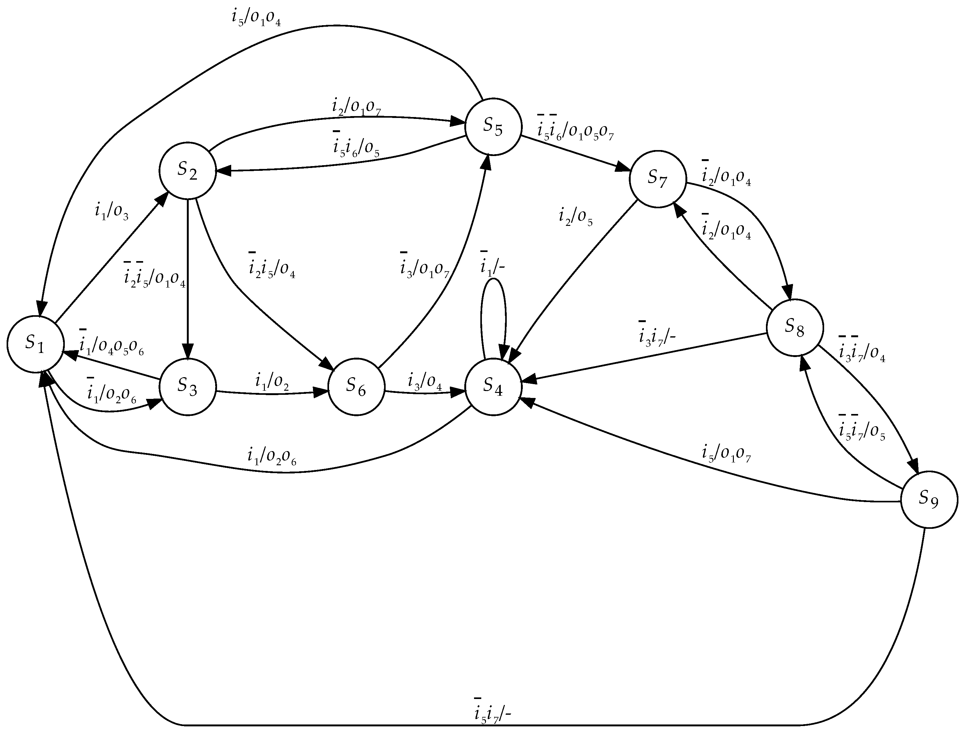
We discuss a synthesis example for Mealy FSM
A1 (
Figure 6). To implement the FSM circuit, we use LUTs with
.
The FSM states correspond to the STG vertices [
17]. To show interstate transitions, the vertices are connected by arcs. An STG includes H arcs. The
h-th arc
is marked by a pair
. In this pair, the symbol
stands for a conjunction of either FSM inputs
or their complements. This is an input signal. The set
includes FSM outputs
generated during the transition number
h.
The STG (
Figure 6) determines the following sets:
,
, and
. Therefore, the FSM
A1 is characterized by
,
. There are 22 arcs in the initial STG. This gives 22 transitions among the states of FSM
A1.
Step 1. This step is omitted if an FSM is represented by STT. The transformation is executed in the following way [
14]. The STT includes H lines. Each line corresponds to an STG arc. Each transition is characterized by its current state
, the next state
, inputs
(for the
h-th arc, this is the signal
), outputs
(for the
h-th arc, this is the OC
), and
h. Therefore, each arc determines the columns
,
,
,
, and
h.
Table 1 is an STT of
A1.
This table uniquely corresponds to the STG (
Figure 6). We add the column
q into
Table 1 to show the subscripts of output collections.
Step 2. The following values of
can be found from the analysis of
Table 1:
for states
,
,
,
,
;
for states
,
,
,
. Additionally,
. Using (
1) gives
. As follows from the initial conditions of the example,
. Therefore, condition (
18) takes place for states with
. Thus, the following sets can be created:
and
. As follows from our analysis, some states may be transferred from
to
S2. Thus, the elements of these sets can be changed. From
Table 1, we can find the sets
and
.
Step 3. Using known approach [
20], we can find the partition
of the set
S1. It includes the classes
and
. Because the set S1 is a preliminary one, this partition is also preliminary. Each class includes
elements. Using (
8) gives the following relation:
. Using (
9) gives
. Therefore, there is a set of state variables
.
Step 4. The classes
determine the following sets of inputs:
and
. Therefore, we have
. This means we cannot add new inputs in these sets due to violation of condition (
10). Each set
can include up to 3 elements without violation of (
10). Therefore, one additional state can be added to each of the sets
.
The method of state redistribution is discussed in detail in the paper [
22]. In our current paper, we just show the result of redistribution, which is the following:
and
. The redistribution gives the following classes:
and
. Now, we obtain
. Using these values and Formula (
8), we can see that
and
. Therefore, the total number of state variables
does not change, but now the set
includes fewer elements. Now we can expect a decrease in the value of the LUT count for the circuit of
CoreFC.
Step 5. There are
elements in the set
S. Therefore, using (
1) gives
. This value determines the sets
and
. As shown in [
17], it is necessary to cover the states from the same class using the minimum possible number of generalized cubes of
R1-dimensional Boolean space. Such an outcome decreases the number of literals in functions (
19)–(
21). One of the possible outcomes is shown in
Figure 6. To encode the states by MBCs, we used the algorithm JEDI [
40].
As we can see from the analysis of the resulting Karnaugh map (
Figure 7), the states
are covered by the generalized cube 00xx. The states
are represented by the generalized cube x100. The cube 1x00 covers the states
. Therefore, for our example, each class is placed into a single generalized cube.
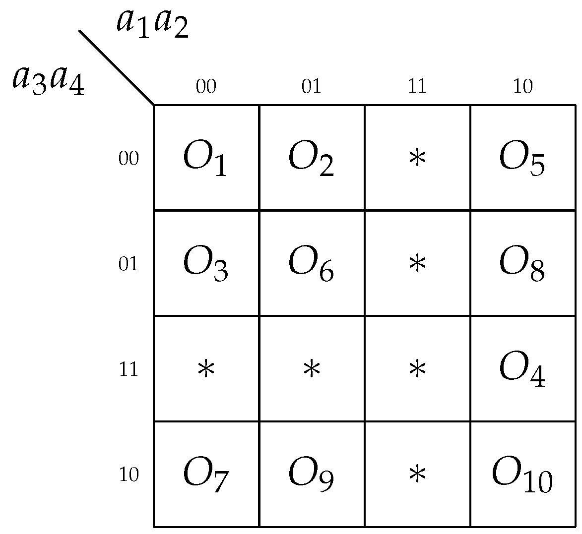
Step 6. The analysis of
Table 1 gives
output collections. They are the following:
,
,
,
,
,
,
,
,
, and
. Using (
5) gives
and the set
.
Each literal in the sum-of-product (SOP) of a Boolean function corresponds to an interconnection between the input source and a corresponding LUT. To reduce the number of interconnections, the number of literals in SOPs should be decreased. To encode the output collections, we used the methods presented in classical work [
17]. Using the approach from [
17] gives the codes shown in
Figure 8.
We encoded the OCs in a way where the variable
is generated only by one LUT of
CoreFC. To do this, we have analyzed
Table 1. The analysis of
Table 1 shows that the following OCs are generated during the transitions from states
:
,
,
, and
. Therefore, we have divided the Karnaugh map (
Figure 8) into two parts. The first part corresponds to
, and the second part corresponds to
. We have placed the OCs
,
,
, and
into the second part. Now, we can obtain the following system of functions:
The SBF (
29) determines the circuit of
LUTerOF. The function
is represented by a corresponding output of
LUTerFA. Therefore, the circuit of
LUTerOF consists of 6 LUTs. Analysis of system (
29) shows that there are 12 literals in the SOPs of the implemented functions. This determines 12 interconnections between
LUTerOF and other circuit blocks. Using the results of [
19] gives the maximum number of interconnections. In our case, it is equal to
. Thus, due to using the proposed approach, the number of interconnects is reduced by 2.33 times.
Step 7. To construct the table of
CoreFC, it is necessary to select the lines of STT with transitions from states
. In the discussed case, we should select lines 1–2 and 6–9 of STT (
Table 1). The table of
CoreFC includes 5 additional columns (compared to the baseline STT). These columns are:
,
,
,
, and
. There is a self-explanatory meaning of columns
and
. The column
includes IMFs creating the code
(to load it into the code register). The column
includes the additional variables
equal to 1 in codes of generated OCs. These variables are also produced by some blocks of
LUTerPC. The column
includes the additional variables
generated only by the block
CoreFC. Obviously, these variables are not produced by any block of
LUTerPC.
Table 2 represents the block
CoreFC for the given example.
The columns
and
are created in the following manner. For example, there is an OC
written in line 1 of
Table 1. Analysis of
Figure 8 gives the code
. This code determines the variables
,
, and
. Therefore, the first line of
Table 2 includes the variables
and
in the column
, as well as the variable
in the column
. All other lines of
Table 2 are created using a similar approach.
Using
Table 2, we can obtain SBFs (
19)–(
21). For example, the function
is represented as the following:
The block CoreFC determines the set . We will show a bit later the SOPs for functions and .
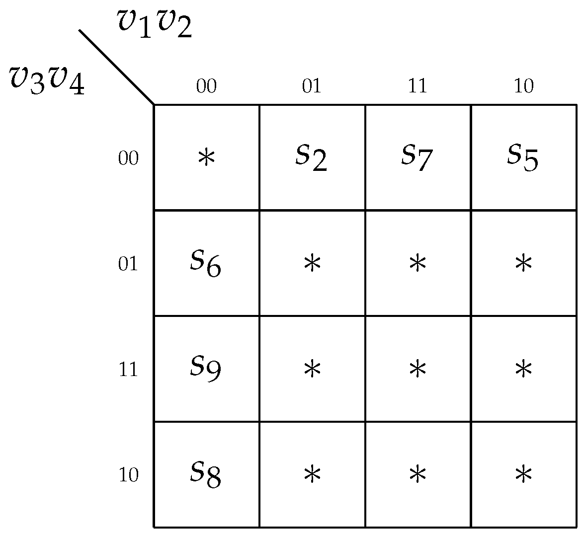
Step 8. The codes for states
use the variables
. The codes for states
are based on the variables
,
. The code combination
indicates that a particular state belongs to a class other than
. The code combination
indicates that a particular state belongs to a class other than
. Due to the fulfillment of condition (
10), the codes do not affect the number of LUTs in the circuit of
CorePC. Therefore, the partial state codes can be arbitrary. We have chosen the following approach: the smaller the subscript (m) of a state, the more nulls its partial code contains. The obtained partial state codes are shown in
Figure 9.
Using
Figure 9, we can obtain the following partial codes:
,
, and
. Using them allows for creating tables representing
CorePC.
Step 9. The block
CorePC includes two blocks of LUTs. The block
corresponds to the set
, whereas the block
corresponds to the set
. The table of
) (
Table 3) is based on lines 3–5, 10–12, and 15–16 (
Table 1).
Table 4 represents the block
. The table is constructed using the lines 13–14 and 17–22 of the initial STT.
In these tables, the current states are represented by their partial codes ; the states of transition are represented by their full codes . The column of STT is replaced by the columns and , respectively. These columns include additional variables equal to 1 in the codes of the OCs.
The transparent approach is used to construct SBFs (
22) and (
23). For example, the functions
,
, and
are represented as:
In the same way, we can obtain the following SOPs:
Step 10. The block
LUTerFA is based on
Table 5.
Table 5 includes the following columns: Function (this is an assembled function produced by
LUTerFA),
CoreFC, and
CorePC. If some function belonging to the set
is generated by a LUT of the block
CoreFC, then there is a 1 in the intersection of the row containing this function and the column
CoreFC. The opposite situation is marked by 0. The column
CorePC is divided by
J subcolumns corresponding to the classes
. The same principle is in play for placing either 1 or 0 in the rows of this part of
Table 5.
Table 5 determines the
R1 +
R2 disjunctions of partial Boolean functions. The following disjunctions represent the circuit of the block
LUTerFA:
Step 11. The block
LUTerASV transforms the full codes
into the partial state codes
. This transformation is not executed for the states
. The table of
LUTerASV includes the following columns:
,
,
, and
. The last column includes the symbols of additional variables equal to 1 in the codes
. In the discussed case, the full state codes are taken from
Figure 7; the partial state codes are taken from
Figure 9. Using these codes, we can create
Table 6.
Obviously, using
Table 6 gives us the perfect SOPs [
17] of SBF (
12). To minimize the number of interconnections between the blocks
LUTerFA and
LUTerASV, we transform
Table 6 into a multi-functional Karnaugh map (
Figure 10).
Figure 10 is based on
Figure 7. This transformation is done in an obvious way. We have simply replaced the symbols of states from
Figure 7 with symbols of corresponding additional variables. Additionally, the codes of states
are “do not care” code combinations. Using
Figure 10 gives us the following SBF:
There are 10 literals in SBF (
34). If each function from (
12) is represented by its perfect SOP, then these SOPs have
literals. Therefore, using the multi-functional Karnaugh map allows for reducing the number of interconnections by 1.6 times. As shown in [
31], the fewer interconnections a circuit has, the less power it consumes.
Step 12. During this step, various technology mapping procedures should be executed [
45,
46]. If the FPGA chip used is produced by AMD Xilinx, then their CAD tool Vivado [
47] should be applied for implementing an FSM circuit. In the next section, we show some results based on using this CAD package to implement FSM circuits. Experiments allow us to compare the effectiveness of the proposed method in relation to some known methods.
At the end of this section, we will show how to estimate the hardware amount in the circuits of FSMs
and
. We start from FSM
. To find the LUT counts for circuits of
CoreFC,
CorePC (the first logic level), and
LUTerFA (the second logic level), it is necessary to analyze
Table 5 (the table of
LUTerFA). Each symbol “1” in this table corresponds to a LUT from the first logic level. In the table, there are 21 “1” symbols. Therefore, the first-level circuits consist of 21 LUTs. If a row of the table includes more than a single 1, then this row corresponds to a LUT from the second logic level. There are 7 LUTs in the circuit of
LUTerFA. This can be found from
Table 5. To find the LUT counts for blocks
LUTerOF and
LUTerASV creating the third logic level, we should analyze SOPs (
29) and (
34), respectively. If an SOP includes at least two literals, then it determines a LUT of the third logic level. As follows from (
29), there are 6 such SOPs. The analysis of (
34) shows that the system includes 4 such SOPs. Therefore, the third logic level includes 10 LUTs. Summing up the number of LUTs for different levels, we see that the circuit of FSM
includes
LUTs.
To estimate the number of LUTs in the circuit of FSM
, it is necessary to find the compatibility classes for the set of states. Using the approach [
20] gives the partition with
. There are the following relations between the classes of
and
:
,
, and
. This means that the table of
LUTerPF (FSM
) is the same as
Table 5. This gives 21 LUTs for the first logic level consisting of the blocks
LUTer1–
LUTer3. Also, there are 7 LUTs in the circuit of
LUTerPF. The blocks
LUTerOF are the same for both FSMs (each of which includes 6 LUTs). However, there is
. This gives 6 LUTs in the block
LUTerASV. In total, 12 LUTs create the third logic level of FSM
. Summing up the number of LUTs for different levels, we see that there are
LUTs in the circuit of
.
Therefore, for such a simple FSM, we see a gain of 5.3% due to the transition from to . For more complex FSMs, the gain can be much higher. This statement is confirmed by the results of the research shown in the next section.
6. Experimental Results
As a basis for comparing the efficiency of different synthesis methods, we use the benchmark FSMs from the library [
42]. The library includes 48 benchmarks of varying complexity (numbers of states, inputs, outputs, output collections, and interstate transitions). The STTs of benchmark FSMs are represented using the format KISS2. These benchmarks have been used by different designers as a representative sample to compare the main characteristics of proposed and known FSM circuits [
33,
34,
36]. To give an idea of the complexity of these benchmarks, we show their characteristics in [
19,
42].
As a rule, in research, FSMs are considered as stand-alone units. In this case, the stability of the output signals is not one of the main design problems. However, in our current paper, we consider Mealy FSMs as some parts of digital systems. As follows, for example, from [
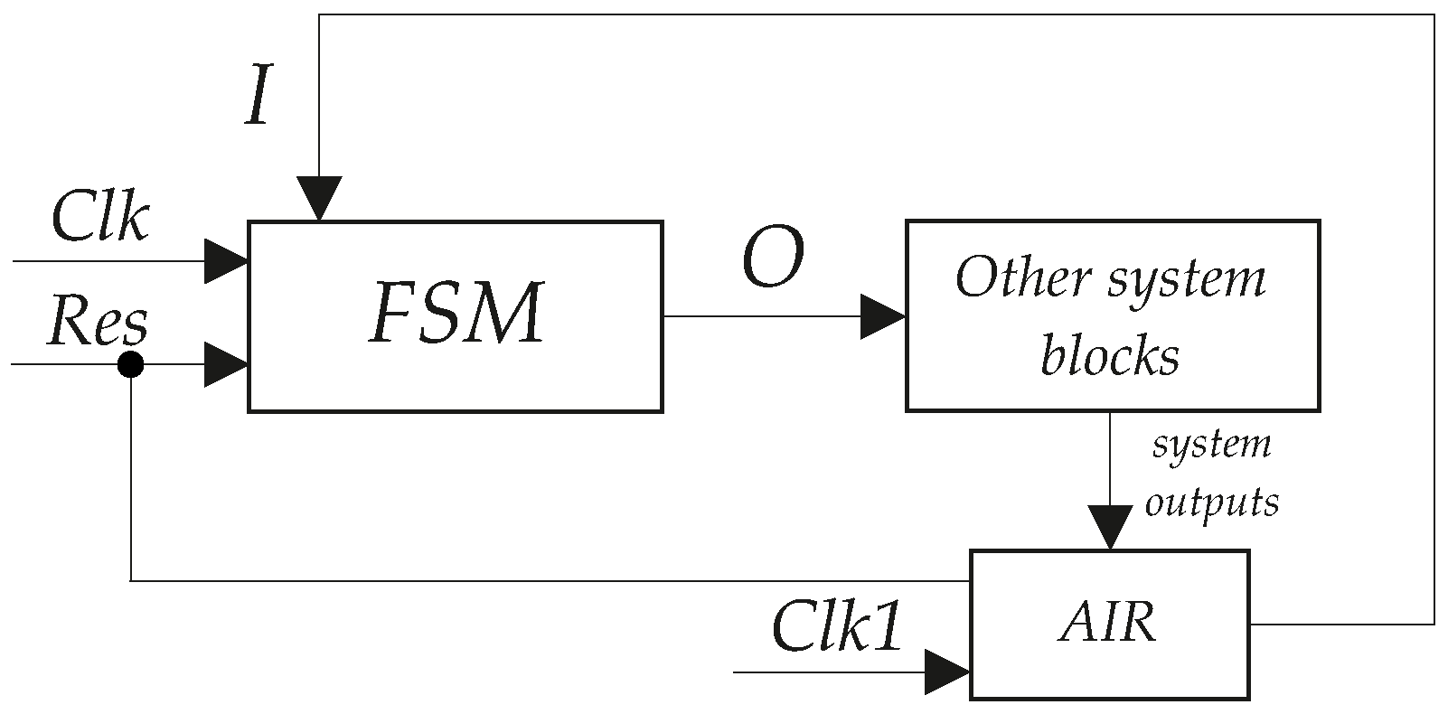
14], Mealy FSMs are unstable. This means that input fluctuations result in output fluctuations. The output fluctuations can cause operation failure in a digital system. Output stabilization can be achieved due to using a synchronous input register (AIR) [
19]. The following is a principle of interaction of an FSM and other digital system blocks (
Figure 11).
The system outputs are treated as FSM inputs forming the set I. As long as there are transients in the digital system, the synchronization signal Clk1 is equal to zero. This actually disconnects the FSM from other system blocks. When system outputs are stable, they are loaded into the AIR. Due to this, fluctuations in the system outputs do not affect the FSM output values. Of course, there is some overhead connected with this approach. Obviously, AIR consumes additional resources of the FPGA fabric. It also consumes some additional power and increases the value of FSM cycle time. Therefore, we took into account this overhead in our research.
In experiments, we use the Virtex-7 VC709 Evaluation Platform (xc7vx690tffg1761-2) [
38]. Its FPGA chip xc7vx690tffg1761-2, produced by AMD Xilinx, is a base for implementing FSM circuits. For LUTs of this chip, there is
. The step of technology mapping is executed by the CAD tool Vivado v2019.1 (64-bit) [
47]. To create tables with experimental results, we use data from the reports produced by Vivado. The VHDL-based FSM models are used to connect the benchmarks with Vivado. We use the CAD tool K2F [
10] to create VHDL codes corresponding to initial KISS2-based benchmark files.
From the Vivado reports, we have derived the following characteristics of
Mealy FSM circuits: the number of LUTs (LUT count), value of cycle time, maximum operating frequency, and power consumption. As a basis for comparison, we have chosen four different FSMs. They are the following: 1.
P Mealy FSMs with MBCs produced by the Auto method of Vivado; 2.
P Mealy FSMs with one-hot state codes produced by the One-Hot method of Vivado; 3. JEDI-based
P Mealy FSMs; and 4.
-based FSMs with twofold state assignment [
20]. We did not compare
and
PY Mealy FSMs. This is because
FSMs have better characteristics than equivalent
PY Mealy FSMs [
20]. Therefore, if the proposed approach allows for improving characteristics compared to
, then the results obtained will obviously be better than the results for equivalent
PY Mealy FSMs.
As follows from [
19,
42], the values of LUT counts and other LUT-based FSM circuits’ characteristics strongly depend on the relation between the values of
and
. In the discussed case, there is
. The benchmarks used have 5 complexity levels (
C0–
C4). These levels are determined in the following order. The benchmarks have the level C0 if
. The level C0 determines trivial FSMs. The benchmarks have the level C1 if
. The level C1 determines simple FSMs. The benchmarks have the level C2 if
. The level C2 determines average FSMs. The benchmarks have the level C3
. The level C3 determines big FSMs. The benchmarks have the level C4 if
. The level C4 determines very big FSMs.
The results of experiments are shown in
Table 7 (the LUT counts),
Table 8 (the minimum cycle times),
Table 9 (the maximum operating frequencies), and
Table 10 (the consumed power). There is a similar organization for each of these tables. Benchmark names are in the table rows. The investigated methods are shown in the table columns. The complexity of a particular benchmark is shown in the last column. The row “Sum” includes results of summation for corresponding columns. In the row “Percentage”, we show the percentage of the summarized characteristics of various FSM circuits with respect to
-based FSMs.
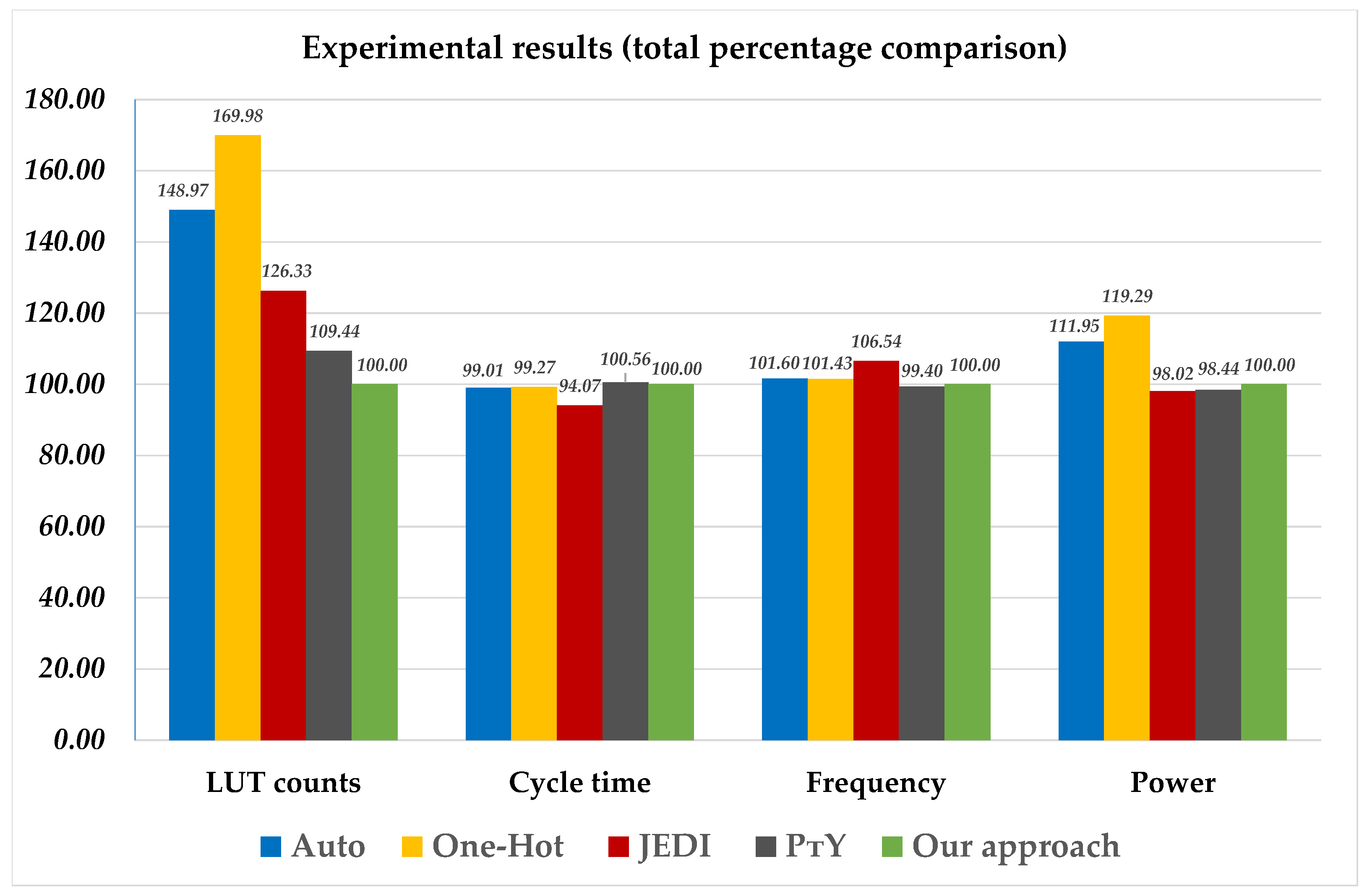
From
Table 7, we can find that, compared to other investigated methods, the circuits of
-based FSMs consume a minimum number of LUTs. The proposed approach provides the following gain: 1. 48.97% regarding the Auto-based FSMs; 2. 69.98% regarding the One-Hot-based FSMs; 3. 26.33% regarding the JEDI-based FSMs; and 4. 9.44% regarding the
-based FSMs. In our opinion, this gain is associated with a decrease in the amount of transformed state codes compared to
-based FSMs. Due to this, the LUT count in
LUTerASV is less than 1 for the code transformer of equivalent
-based FSMs. Additionally, the gain can be achieved due to reducing the cardinality number of the partition of states. The fulfillment of the condition
provides a decrease in the required number of LUT inputs for elements of
LUTerFA compared to that of the LUTs of
LUTerPF. This phenomenon can lead to a decrease in the LUT count.
The following phenomenon is clear from
Table 7: if an FSM has the complexity C0, then there are the same LUT counts for equivalent FSMs based on collection encoding. Moreover, in this case, other FSMs have better values of LUT counts than
- and
-based FSMs. We can explain this in the following way. If an FSM has the complexity C0, then the condition (
4) takes place. In this case, each SOP (
2) and (
3) is implemented by a single LUT. Therefore, in this case, there is no need to use various structural decomposition methods. However, regardless of the validity of condition (
4), the encoding of output collections is executed for both
- and
-based FSMs. As a result of this, the block
LUTerOF is used. This block consumes additional LUTs compared to other researched methods. Due to validity of (
4), there are no partial functions for FSMs having the complexity C0. As a result, there is no need to assemble blocks (
LUTerFA and
LUTerPF). This means that both
and
FSMs degenerate into equivalent
PY FSMs.
Now, let us analyze the temporal characteristics of FSM circuits. They are represented in
Table 8 (the cycle time measured in nanoseconds) and
Table 9 (the maximum operating frequency measured in megahertz).
Analysis of
Table 8 shows that JEDI-based FSMs are the fastest. It also shows that
-based FSMs are marginally slower than circuits of
-based FSMs (the average loss is 0.56%). At the same time, the proposed approach generates circuits with worse time characteristics than the circuits of
P FSMs. The Auto-based FSMs are 0.09% faster than the
-based FSMs. The One-Hot-based FSMs are 0.73% faster than the
-based FSMs. Finally, JEDI-based FSMs are 5.93% faster than
-based FSMs. If the FSM complexity exceeds C0, then both
- and
-based FSMs have three-level circuits. At the same time, it is difficult to estimate a priori the number of logic levels in circuits of
P FSMs. It all depends on the number of literals in the implemented sum-of-products.
As follows from
Table 8, if FSM complexity is equal to C0, then cycle times are the same for equivalent
- and
-based FSMs. This phenomenon takes place because, in this case, both
- and
-based FSMs turn into
PY FSMs. However, if we look at the most complex FSMs having the complexity C4, we will see that the proposed method allows for obtaining the fastest circuits. Thus, the performance of
FSMs becomes better and better as the synthesized FSMs become more complex.
As follows from
Table 9, an average, the circuits of
FSMs are slower compared to circuits of P-based FSMs. Our approach loses 1.6% to Auto-based FSMs. It loses 1.43% to One-Hot–based FSMs. The JEDI-based FSMs have the greatest gain (6.54%). Only
-based FSMs are a bit slower than
-based FSMs. Obviously, the reasons for the loss in frequency are the same as the reasons for the loss in cycle time. Additionally, analysis of
Table 9 shows that, starting with complexity level C2, our method allows us to produce faster circuits compared to other methods under study.
It is known [
48] that one of the most important characteristics of FSM circuits is their power consumption. In particular, it is important in the case of mobile and autonomous cyber-physical systems [
49]. Very often, a designer should make the choice among the area-temporal characteristics and the power consumption of a particular device. The values of power consumption can be taken from the Vivado reports. The power consumption is measured for the maximum possible value of the operating frequency. We show the experimental results for power consumption in
Table 10.
The proposed method reduces the numbers of LUTs in FSM circuits compared with this characteristic of equivalent
-based FSMs. Very often, such improvement results in an increase in power consumption [
19]. This phenomenon takes place for our method. However, as follows from comparison of
- and
-based FSMs (
Table 10),
FSMs have a very small gain in power consumption. Compared to
-based FSMs, the loss in power consumption averages 1.55%. Additionally, JEDI-based FSMs require less power than equivalent
FSMs. The proposed approach allows for obtaining FSM circuits with less power consumption than for both Auto-based FSMs (11.95% of gain) and One-Hot-based FSMs (19.29% of gain).
If FSMs have complexity C0, then both
and
FSMs have equal values of power consumption. If the FSM complexity exceeds C0, then
FSMs always require less power than equivalent
FSMs. We see the following reason for this situation. In
FSMs, the state variables enter only block
LUTerASV. In contrast to this, in
FSMs, the outputs of
LUTerFA are connected with two blocks (
LUTerASV and
CoreFC). It is known [
31] that interconnections consume up to 70% of power. Therefore, the more interconnections, the more power is consumed.
Let us sum up some results of the comparison of equivalent
and
FSMs. If FSMs have complexity C0, then there are the same values of basic characteristics for both models. For other levels of complexity,
FSMs have better spatial characteristics (the required FPGA chip area) than they do in their single-core counterparts based on twofold state assignment. For rather simple FSMs,
FSMs have better temporal characteristics. However, as the complexity increases, the cycle times (and maximum operating frequencies) of
FSMs gradually become better than in their single-core counterparts. The FSM circuits based on the proposed method always require more power. However, this loss is very small (it does not exceed 2% on average). This comparison leads to the following conclusion:
FSMs should be used instead of
FSMs if the required chip area is the main optimality criterion of designed LUT-based circuits. This conclusion is supported by diagrams shown in
Figure 12.
Under certain conditions, the proposed method can be applied to implement the LUT-based circuit of any sequential block. In this case, neither the algorithm for the functioning of this block nor the scope of the digital system in which this block operates is important. The possibility of applying the model of
FSM depends on the distribution of inputs
between the states
. If this distribution leads to the fulfillment of condition (
4), then there is no need for optimization (because the circuit of
P FSM has the best possible characteristics). If condition (
4) is violated but the distribution leads to the fulfillment of condition (
10), then the method can be applied. Otherwise, it is impossible to find a partition of the set of states for which each partial function is represented by a single-LUT circuit. The proposed method can be applied only if condition (
18) is satisfied for some states
. In this case, the corresponding partial functions depending on the state variables
are implemented using single-LUT circuits. The more states that satisfy condition (
18), the greater the gain from applying our method compared to using
FSMs. However, if condition (
18) is satisfied for all states, then there is no point in applying either
or
FSMs. In this case, both of these models degenerate into a
PY FSM. Thus, it is advisable to use the proposed method only if condition (
18) is satisfied for a number of states (but not for all M states), and condition (
10) for the rest.
7. Generalized FSM Architecture
Unfortunately, there is a condition where the proposed method cannot be applied. For a given FSM, let the set of states include at least a single state
for which the following condition is satisfied:
It is obvious that the state satisfying condition (
35) cannot be included in either set
or set
S1. To obtain partial functions generated during transitions from this state, it is necessary to apply the methods of functional decomposition. Thus, to take into account the presence of such states, it is necessary to introduce a
CoreFD based on functional decomposition into the architecture of
FSM shown in
Figure 5.
We propose to split the set
S by three disjoint sets (
,
,
). The set
includes states satisfying condition (
18). The set
includes states satisfying condition (
35). The set
includes the rest of the states, i.e.,
. The transitions from states
are determined by FSM inputs creating the set
I3. To encode these states, it is necessary to create the set of state variables
ASV3. This set includes its own unique state variables. Three sets of PBFs are generated by LUTs of
CoreFD:
(IMFs generated during the transitions from states
);
(additional variables encoding the OCs generated during the transitions from states
); and
AV3 (unique additional variables encoding the OCs generated during the transitions from states
). Therefore, the following partial SBFs are generated by LUTs of
CoreFD:
We denoted as
the proposed generalized architecture of the LUT-based FSM circuit. Here the letter “F” means the presence of the block
CoreFD. The proposed generalized architecture is shown in
Figure 13.
The generalized architecture (
Figure 13) includes three cores of PBFs.
CoreFC generates PBFs for states satisfying condition (
18).
CoreFD generates PBFs for states satisfying condition (
35).
CorePC generates PBFs for the rest of the states.
In the
FSM,
LUTerFA generates the full functions represented by the following systems of disjunctions:
LUTerOF implements SBF (
7). However, now the set AV is represented in the following form:
. To encode the states of a
FSM, the set
is used, where
. Therefore,
LUTerASV generates the SBF:
Naturally, the proposed architecture is universal. In this paper, we propose the following method for synthesizing an FSM with a generalized architecture:
Creating an STT of a P Mealy FSM.
Pre-formation of sets , S2, and S3.
Pre-formation of partition of set S2.
Final formation of sets and S2 and partition .
Creating full state codes for states .
Encoding of output collections
and finding SBF (
7).
Creating a table of
CoreFC and deriving SBFs (
19)–(
21).
Encoding of states by partial state codes .
Generating tables describing the blocks of
CorePC and deriving systems (
22) and (
23).
Encoding of states by partial state codes .
Generating tables describing the blocks of
CoreFD and deriving systems (
36)–(
38).
Creating a table of
LUTerFA and SBFs (
39) and (
40).
Creating a table of
LUTerASV and system (
41).
Implementing a Mealy FSM circuit using internal resources of a particular FPGA chip.
We hope that all the presented steps of this method are clear from the previous text. We do not, however, consider this method in detail. This will be the subject of a separate study. Now we will show that the generalized architecture (
Figure 13) generates 6 more architectures. Three conditions are used for this purpose. The fulfillment of condition (
18) indicates the presence of the block
CoreFC in the FSM circuit architecture. This means that the set
contains at least one element. The fulfillment of condition (
35) indicates the presence of the block
CoreFD. In this case, the set
S3 contains at least one element. Finally, the fulfillment of the condition
indicates the presence of the block
CorePC. In this case, the set
S2 contains at least one element. We show the possible FSM models in
Table 11. Additionally, the table rows contain conditions (or their conjunctions) in which a particular architecture should be used.
The first three columns of the table contain the names of the sets (, , ) and corresponding architectural blocks (CoreFC, CorePC, CoreFD). The fourth column contains the model designation. The fifth column shows which combination of conditions leads to the model from a particular row. If there is a zero (one) at the intersection of the column with the block and the row with the model, then this block is not included (is included) in the FSM architecture corresponding to this row.
For example, if all states satisfy condition (
35), then the architecture includes only
CoreFD. We denote this architecture by the symbol
. This is the first row of
Table 11. If some of states satisfy condition (
35) and others satisfy condition (
42), then the architecture includes blocks
CorePC and
CoreFD (row 3). This leads to
FSMs, and so on. The last row corresponds to the generalized FSM architecture, including three cores of partial functions.
Using
Table 11 and generalized architecture, we can obtain the architecture for any model represented by this table. Obviously, it is possible to transform the design method for
FSMs into a design method for any other model. In this case, of particular interest is the implementation of Step 2 of the proposed method and the definition of a model corresponding to its outcome. We have presented the algorithm for performing these steps in
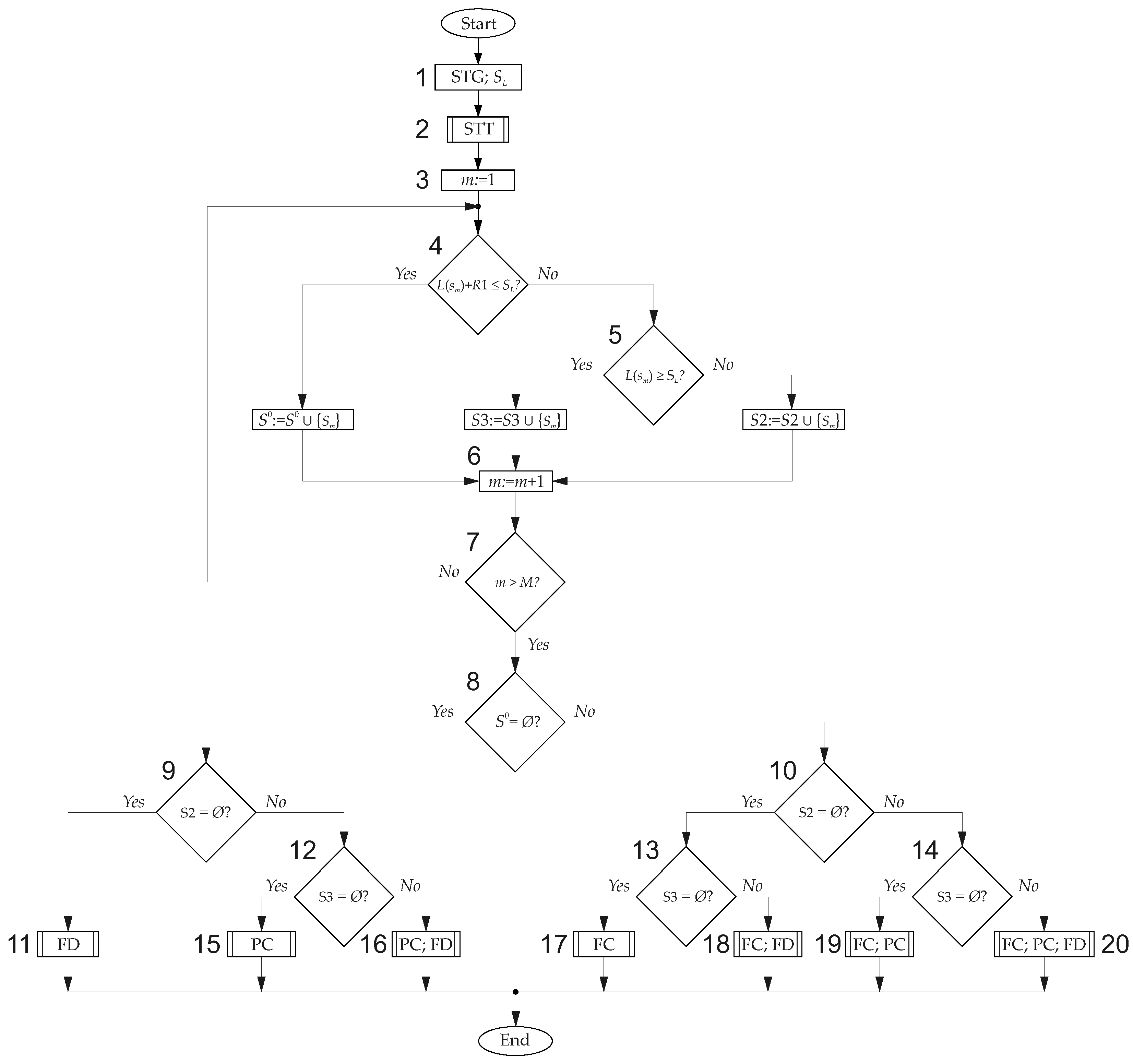
Figure 14.
Let us consider this algorithm. Block 1 shows the initial information (FSM is represented by STG and the FPGA chip is represented by the number of inputs of the LUT element). Next, this STG must be converted to the equivalent STT (block 2).
The distribution of states over sets
is performed in a cycle, including blocks 3–7. The distribution starts from the first state (block 3). In block 4, condition (
18) is checked. If this condition is met (output “Yes” from block 4), then the state
is placed in set
(block FC). If this condition is violated (output “No” from block 4), then condition (
42) is checked (block 5). If this condition is met (output “Yes” from block 5), then the state
is placed in set
S3 (block FD). If this condition is violated (output “No” from block 5), then the state
is placed in set
S2 (block PC). The analysis of the next state begins (block 6). If all states are distributed (output “Yes” from block 7), then the FSM architecture selection begins (transition to block 8). Otherwise (output “No” from block 7), the analysis continues (transition to block 4).
To choose an architecture, we analyze whether empty sets are obtained in the process of distributing states. The analysis begins with checking the set
(block 8). As follows from
Table 11, if the set
is empty (output “Yes” from block 8), then the choice is made among three architectures (
,
,
). Set
S2 is analyzed (block 9). If it is empty (output “Yes” from block 9), then the FSM
is selected (block 11). If set
S2 is not empty (output “No” from block 9), then set
S3 is analyzed (block 12). If it is empty (output “Yes” from block 12), then the FSM
is selected (block 15). If set
S3 is not empty (output “No” from block 12), then the FSM
is selected (block 16).
If the set is not empty (output “No” from block 8), then the choice is made among four architectures (, , , ). Set S2 is analyzed (block 10). If it is empty (output “Yes” from block 10), then set S3 is analyzed (block 13). If S3 is empty (output “Yes” from block 13), then the FSM PY is selected (block 17). If S3 is not empty (output “No” from block 13), then the FSM is selected (block 18). If set S2 is not empty (output “No” from block 10), then set S3 is analyzed (block 14). If S3 is empty (output “Yes” from block 14), then the FSM is selected (block 19). If S3 is not empty (output “No” from block 14), then the FSM is selected (block 20).
Thus, the architecture has been chosen, and it is necessary to proceed to the synthesis of the corresponding FSM model. We hope that the relationship between
Table 11 and the algorithm (
Figure 14) is transparent enough.


