Abstract
Out-of-plane p-n heterojunctions based on two-dimensional layered materials (2DLMs) with unusual physical characteristics are attracting extensive research attention for their application as photodetectors. However, the present fabrication method based on 2DLMs produces out-of-plane p-n homojunction devices with low photoresponsivity and detectivity. This work reports an ultrasensitive phototransistor based on a laser-induced p-doped WSe2/MoS2 van der Waals heterojunction. The laser treatment is used for p-doping WSe2 nanoflakes using high work function WOx. Then, an n-type MoS2 nanoflake is transferred onto the resulting p-doped WSe2 nanoflake. The built-in electric field of p-doped WSe2/MoS2 is stronger than that of pristine WSe2/MoS2. The p-n junction between p-doped WSe2 and MoS2 can separate more photogenerated electron–hole pairs and inject more electrons into MoS2 under laser illumination than pristine WSe2/MoS2. Thus, a high photoresponsivity (R) of ~1.28 × 10⁵ A·W−1 and high specific detectivity (D*) of ~7.17 × 10¹³ Jones are achieved under the illumination of a 633 nm laser, which is approximately two orders higher than the best phototransistor based on a WSe2/MoS2 heterojunction. Our work provides an effective and simple method to enhance photoresponsivity and detectivity in two-dimensional (2D) heterojunction phototransistors, indicating the potential applications in fabricating high-performance photodetectors based on 2DLMs.
1. Introduction
Photodetectors are critical elements of emerging technologies, such as autonomous vehicles, environmental monitoring systems, security systems, mobile phone cameras and telecommunications systems [1,2]. The most common types of photodetectors are photodiodes and phototransistors. A photodiode works by developing a p-n junction or Schottky junction, which separates the photoinduced electron–hole pairs, causing the generated electrons and holes to move in opposite directions, culminating in a photocurrent or photovoltage. In a phototransistor, electron–hole pairs are primarily separated by external bias and further regulated by a gate, resulting in a photocurrent. Photodetectors based on two-dimensional (2D) material heterostructures have remarkable responsivity, which has been confirmed through theoretical simulation models [3,4]. Most importantly, out-of-plane 2D van der Waals heterostructure phototransistors can combine the advantages of photodiodes and phototransistors. The operation schematics of a photodiode and phototransistor are shown in Figure S1a,b in the Supporting Information, respectively. In the heterostructure phototransistor configuration, the photodiode (p–n junction) part separates electron–hole pairs under light illumination, in which electrons are injected to MoS2, resulting in maximizing its electrical response to light in terms of photogain, as shown in Figure S1c. The phototransistor also minimizes the noise in its electrical output by operating the device in the depletion regime using appropriate gate voltage modulation.
Recently, phototransistors based on WSe2 and MoS2 have shown promising avenues for optoelectronic devices, with promising carrier transport properties, high on/off ratio, high light absorption coefficient, scalable thickness down to the monolayer and, most significantly, easy to introduce doping [2,5,6,7,8,9,10,11]. However, these devices have shown limited photoresponsivity and detectivity due to the weak built-in electric field formed between WSe2 and MoS2 [6,9,10]. Therefore, further investigations regarding improvements in the strength of a built-in field for boosting the performance of the phototransistor based on WSe2/MoS2 are still needed.
Among 2D transition metal dichalcogenides (TMDs), p-doping techniques have been widely reported as an effective tool to manipulate the properties of heterostructure phototransistors, including chemical doping with XeF2 vapors, PPh3/AuCl3, low-energy phosphorus implantation, Te and H2 gas, electrostatic split-gate configuration, ozone treatment and UV/ozone treatments [11,12,13,14,15,16,17]. Additionally, n-doping techniques have also been reported, including electron beam lithography, self-assembled monolayer, triphenylphosphine, lithium fluoride, nitrogen, zinc oxide and alkali metal compound-promoted chemical vapor deposition (CVD) [18,19,20,21,22,23,24,25]. However, none of these methods can simultaneously achieve controllable, scalable and stable performance over an extended period without introducing chemical impurities. This severely limits the application of optoelectronic devices based on TMDs. Nevertheless, laser treatment has been used for defining p-n heterojunctions for fabricating high-performance photodetectors. It is a simple, efficient and selective p-doping approach for 2D TMDs [5,26,27].
In this study, the laser treatment technique is used for the achievement of p-doping WSe2, forming a strong built-in electric field between p-doped WSe2 and untreated MoS2 in the p-doped WSe2/MoS2 van der Waals heterojunction. The resulting p-doped WSe2/MoS2 heterojunction phototransistor has a high photoresponsivity of ~1.28 × 10⁵ A·W−1 and specific detectivity of ~7.17 × 10¹³ Jones, which are significantly higher than those of the reported MoS2 and WSe2/MoS2 field-effect transistors (FETs) [1,2,6,8,28]. Our work opens a new avenue for high-performance photodetectors based on two-dimensional heterojunction phototransistors.
2. Materials and Methods
2.1. Multilayer WSe2/MoS2 Preparation
The WSe2 and MoS2 nanoflakes were first exfoliated from their crystal (HQ graphene company) by using blue tapes. The multilayer WSe2 was fabricated through repeated tape exfoliation and transferred to a p++ Si substrate with a 90 nm SiO2 capping layer. In contrast, the multilayer MoS2 was directly prepared on a polydimethylsiloxane (PDMS) substrate, supported by a glass slide. Atomic force microscopy (AFM, Dimension 3100, Veeco, Plainview, NY, USA) and optical microscopy (Keyence VHX-600, Osaka, Japan) were used to measure and screen the shapes and thickness of WSe2 (MoS2), respectively. When conducting these experiments, the surface of WSe2 and MoS2 should be clean. The area of MoS2 nanoflakes needs to be larger than WSe2 to completely cover the underlying WSe2.
2.2. Laser-Scanned Process
Multilayer WSe2 was scanned via Raman spectrometer laser (Renishaw in via Raman microscope) to fulfill region-selectable p-type doping. To figure out the proper power and exposure time for p-doping, multilayer WSe2 was scanned with 633 nm, 515 nm and 473 nm lasers. The laser power and exposure time were set in a series of gradients. The diameter (d) of the 633 nm laser beam was calculated as 0.61 µm by d = K·λ/NA, where K = 0.82 was used for a Gaussian beam, λ = 633 nm was the laser wavelength and NA = 0.85 was the numerical aperture of the objective; the diameters of 515 nm and 473 nm laser beam were 0.50 and 0.47 µm, respectively. The laser scanning step size was set as 0.3 µm. Then, the pristine WSe2 and laser-scanned WSe2 were measured via Raman spectrometer (Witec Alpha 300 Access, Ulm, Germany) with a 532 nm laser. Laser power was set to 0.5 mW to avoid doping effect on WSe2. The integration time was 8 s, and the number of integrations was 3. The experiment details are shown in Supporting Information Figure S2 and Table S1. After the preliminary experiment with the laser-scanned process, another WSe2 was scanned using 633 nm laser, with laser power of 4 mW, exposure time of 0.75 s and laser spot diameter of 0.61 µm.
2.3. Polydimethylsiloxane (PDMS)-Assisted Transfer
The PDMS supporting the specific MoS2 was carefully cut into 1 mm × 1 mm pieces without tearing up the MoS2 to avoid stress shredding MoS2/MoS2 heterojunction in the PDMS-assisted transfer process. After the laser-scanned process of WSe2, the specific MoS2 was accurately transferred onto the WSe2 by using a dry transfer system (E1-T multifunctional high-precision 2D material transfer system from Metatest Corporation Company, Las Vegas, NV, USA). The fabricated WSe2/MoS2 heterojunction was soaked in acetone at 40 °C for ten mins to remove uncrosslinked oligomers of PDMS that remained on the surface of MoS2, followed by isopropanol soaking and blow-dry process.
2.4. Device Fabrication
Device fabrication consists of several steps: spin coating, photolithography, surface treatment, electron beam evaporation deposition, lift-off and annealing treatment. In the spin-coating process, the WSe2/MoS2 heterojunction was coated with ultraviolet photoresist (LOR, Microchem company, Austin, TX, USA) at 5000/min rotation for 1 min and baked at 180 °C for 10 min. Then, the WSe2/MoS2 heterojunction was coated with ultraviolet photoresist (RZJ-304-25, Ruihong Electronic Chemicals Co., Ltd., Milpitas, CA, USA) at 5000/min rotation for 1 min and baked at 115 °C for 1 min. In the photolithography process, source and drain electrodes are patterned via lithography (Microwriter ML3 laser direct-writing system) on MoS2 at a laser dose of 160 mJ·cm−2. Then, the WSe2/MoS2 heterojunction was soaked in developer solution for 30 s, followed by deionized water soaking and blow-dry process. In the surface treatment process, the WSe2/MoS2 heterojunction was treated in Ar-plasma with at 4 mTorr for 1 min by using a plasma cleaner (Harrick PDC-002, NY, USA) to remove the remained photoresist. In the electron beam evaporation deposition process, 5 nm Ni and 50 nm Au were deposited by the electron beam evaporator (GX1350 from Tianxingda Vacuum Coating Equipment Co., Ltd, Shenzhen City, China). In the lift-off process, the WSe2/MoS2 heterojunction was soaked in N-Methylpyrrolidone (NMP) at 40 °C for 30 min, followed by isopropanol soaking and blow-dry process. In the annealing treatment process, the WSe2/MoS2 heterojunction was annealed at 300 °C in an Ar atmosphere for 2 h by using a tube annealing furnace (OTF-1200X-S from HF-kejing Equipment Co., Ltd., Hefei City, China) to realize better contact. The device fabrication process is shown in Figure S3 in the Supporting Information.
2.5. Optical Characterization
The fabricated MoS2/WSe2 heterojunction on the SiO2/Si substrate was characterized using Raman and photoluminescence (PL) spectroscopy (Witec Alpha 300 Access, Ulm, Germany) with a 532 nm laser. In the Raman measurements, the laser power was set to 0.2 mW to avoid doping effect on WSe2, the integration time was 5 s and the number of integrations was 2. For the PL measurements, the laser power was set to 0.5 mW, the integration time was 8 s and the number of integrations was 3. Optical microscopy (Keyence VHX-600, Osaka, Japan) and atomic force microscopy (AFM, Dimension 3100, Veeco, Plainview, NY, USA) were used to identify the device’s surface topography and step height, respectively.
2.6. Electrical Characterization
All the electric measurements were conducted with a semiconductor parameter analyzer (Agilent, Santa Clara, CA, USA, B1500A). Scanning photocurrent microscopy (SPCM) analysis system combines the electrical characterization system (Agilent B1500A) and the Raman system (Renishaw in Via, Gloucestershire, UK) using a motorized XYZ stage. The semiconductor diode laser (633 nm, Renishaw in Via, Gloucestershire, UK) was focused onto the device’s channel region utilizing a long working distance objective lens with a 50× magnification (NA = 0.5). A mechanical chopper (BET-ES from Beijing Nbet Technology Co., Ltd., Beijing, China) and an oscilloscope (Agilent 86100A) were employed to analyze the time-dependent photoresponse. The hysteretic behavior of the device transfer curve in the air environment can be effectively removed by alternating current pulse scanning (Alternating Polarity, AP) by changing the polarity of the gate voltage, which was applied to transistors of various channel materials [29,30]. Short gate voltage (VG) pulses were applied to the device to obtain the transfer characteristics with and without illumination.
3. Results and Discussion
3.1. Optical Characterization
A 3D (three-dimensional) schematic diagram, 2D schematic diagram of the operation principle and an optical image of the phototransistor based on laser-scanned WSe2/MoS2 van der Waals heterojunction are shown in Figure 1a–c, respectively. The MoS2 and WSe2 nanoflakes were exfoliated onto PDMS and SiO2 substrates, respectively. The WSe2 surrounded by a white dotted-line triangle in Figure 1c was fully scanned using a 633 nm wavelength laser. After the laser-scanned process, MoS2 nanoflakes were transferred onto the surface of laser-scanned WSe2. Source and drain electrodes were patterned via lithography on MoS2 and then 5 nm Ni and 50 nm Au were deposited by the electron-beam evaporator, followed by the lift-off process. Figure 1d presents the height profiles measured using AFM (Supporting Information, Figure S4). The thicknesses of pristine MoS2 and WSe2 and the heterojunction were 5 nm. This shows a consistent thickness. It has been shown that the ambipolar transfer characteristic of the pristine WSe2 field-effect transistor (FET) was converted into unipolar p-type behavior after laser-scanning treatment according to our former works [5,27]. The laser-oxidized product WOx is responsible for the p-type doping of WSe2 [5,27]. The laser-scanned method can also be used for p-doping MoTe2 [26,31].
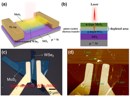
Figure 1.
Phototransistor based on laser-scanned WSe2/MoS2 van der Waals heterojunction: (a) three-dimensional (3D) schematic diagram of the phototransistor; (b) two-dimensional (2D) schematic diagram of the phototransistor’s operation principle; (c) optical microscopy image of the phototransistor; (d) atomic force microscopy image (AFM) of the phototransistor.
In order to establish the proper power and exposure time for p-doping, multilayer WSe2 samples with laser treatment of different power and exposure time were measured (Supporting Information Figure S2 and Table S1). As shown in Figure S2c, the PL peak intensity of WSe2 decreased with exposure time, suggesting effective oxidation originating from serious damage to the structure. As shown in Figure S2e, the PL peak intensity of WSe2 increased with the 633 nm laser-scanned power, indicating a photo-induced enhancement in the electron concentration. After elaborative comparison, the 633 nm laser (laser power of 4 mW, exposure time of 0.75 s) was chosen for controllably p-doping the WSe2.
Figure 2a shows the Raman spectra of multilayer WSe2, MoS2 and the overlapping region between laser-scanned WSe2 and MoS2. The corresponding fitting curves are shown in Supporting Information Figure S5; one strong peak (248 cm−1) and four weak peaks (306, 357, 371 and 392 cm−1) can be observed from WSe2′s Raman spectra, and two strong peaks (381 and 406 cm−1) can be observed from MoS2′s Raman spectra. The Raman spectra of the overlapping area show three strong peaks at 248 cm−1, 381 and 406 cm−1, which means that the laser-scanned WSe2/MoS2 heterostructure is successfully conducted [6]. However, the Raman peak intensities of the MoS2 are reduced for the laser-scanned WSe2/MoS2 heterojunction. These intensity reductions can be attributed to ultrafast charge transfers due to strong interfacial coupling in these structures between laser-scanned WSe2 and MoS2 [32,33]. Furthermore, we conducted the PL spectra of pristine WSe2, MoS2 and laser-scanned WSe2/MoS2 heterojunction, as shown in Figure 2b. Two prominent emission peaks of MoS2 are observed at 1.82 and 1.95 eV, corresponding to emissions originating from the indirect transition and A exciton, respectively. PL of WSe2 also exhibited an indirect transition and A exciton at 1.44 and 1.61 eV, respectively. In the laser-scanned WSe2/MoS2 heterojunction, the PL peak intensity of MoS2 dropped, which indicates charge transfer between p-doped WSe2 and MoS2 [32]. In order to reveal the effect of doping, we fabricated a new WSe2/MoS2 heterojunction with undoped and doped regions. PL intensity of WSe2 and MoS2 both increase obviously in the doped region compared to the undoped WSe2/MoS2 heterojunction, which suggests this carrier density is enhanced through a controllable doping process (see Supporting Information Figure S6).
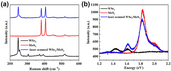
Figure 2.
Raman spectra characterization of the laser-scanned WSe2/MoS2 heterojunction. (a) Raman spectra of WSe2, MoS2 and laser-scanned WSe2/MoS2 heterojunction. (b) photoluminescence (PL) spectra of WSe2, MoS2 and laser-scanned WSe2/MoS2 heterojunction.
3.2. Electrical Characterization
We further conducted electrical measurement of the device. The sublinear IDS (drain current) −VDS (drain voltage) characteristics of a p-doped WSe2/MoS2 heterojunction transistor in Figure 3a indicate the ohmic contacts at source and drain terminals. The IDS−VG characteristic of the p-doped WSe2/MoS2 heterojunction transistor in Figure 3b shows an on/off of ~107, which is comparable to that of the best MoS2 transistors [2,6,8,17,28,34]. The gate insulator capacitance, Cg, for the 90 nm SiO2 and 5 nm WSe2, is calculated to be 3.77 × 10⁻⁸ F·cm−2, using the following formula:
where CSiO2 = 3.84 × 10⁻⁸ F·cm−2 is capacitance of 90 nm SiO2, CWSe2 = 2.07 × 10⁻⁶ F·cm−2 is capacitance of 5 nm WSe2 (COX = ɛ0ɛOX/tOX; ɛSiO2 = 3.9; ɛWSe2 = 11.7; tSiO2 = 90 nm; tWSe2 = 5 nm; where ɛ0 is the vacuum permittivity, ɛOX is relative permittivity, tOX is gate insulator thickness). The field-effect mobility (µ) of the phototransistor is 32.74 cm2/V·s according to the following formula:
where L = 8.95 µm is channel length of the device, W = 24.07 µm is channel width of the device and gm-max = 1.66 × 10⁻⁵ S is maximum transconductance according to the dark transfer curve, VDS = 5 V. We further examined the transfer characteristics of a few-layer WSe2 FET on the 90 nm SiO2/Si substrate, and the IDS−VG transfer characteristics before and after laser-scanned process (using 633 nm laser, with laser power of 4 mW, exposure time of 0.75 s and laser spot diameter of 0.61 µm) are shown in Supporting Information Figure S7. The IDS−VG transfer characteristics are transferred from ambipolar to unipolar p-type apparently, which indicates that WSe2 is effectively p-type doped through the laser-scanned process. This can help to promote a strong built-in electric field between the laser-scanned WSe2 and MoS2.
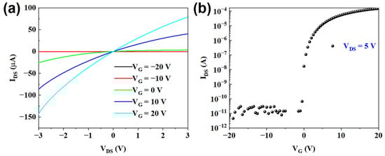
Figure 3.
Electrical characteristics of laser-scanned WSe2/MoS2 field-effect transistor (FET). (a) Output characteristics of laser-scanned WSe2/MoS2 FET. (b) Transfer characteristics of laser-scanned WSe2/MoS2 FET. IDS (drain current), VDS (drain voltage), VG (gate voltage).
3.3. Photoresponse
After the electrical characterization of a p-doped WSe2/MoS2 heterojunction transistor, its photoresponse measurements were also conducted. The device was measured under spot illumination with a 633 nm laser at different power intensities to investigate its photoresponsivity. The scanning photocurrent microscopy (SPCM) method was used to obtain a spatial-resolved photoresponse of the device. SPCM is performed at VDS = 0 V, VG = 0 V and an incident power of 1.94 μW. As shown in Figure S8, the photocurrent of the p-doped WSe2/MoS2 heterojunction is small because the photogenerated carriers cannot be effectively collected using source and drain electrodes under no bias (VDS = 0 V) conditions. To obtain more obvious photocurrent responsivity, SPCM was performed at VDS = 5 V, VG = −10 V and an incident power of 1.94 μW. As shown in Figure 4a, the IDS at a p-doped WSe2/MoS2 heterojunction is much stronger than that at nearby areas, owing to the stronger capability of separating the photogenerated electron–hole pairs in the built-in electric field of the p-doped WSe2/MoS2 heterojunction. Figure 4b shows the transfer curves of a p-doped WSe2/MoS2 heterojunction transistor without and with laser-beam illumination. The IDS of the p-doped WSe2/MoS2 heterojunction increases with the laser-beam illumination intensity. The increasing laser-beam illumination intensity can produce more photoexcited electron–hole pairs after separating through the built-in electric field of the p-doped WSe2/MoS2 heterojunction, more electrons can transfer to MoS2 and then can be effectively collected with the drain electrode, eventually forming the increasing photocurrent. The photoexcited holes are transferred to p-doped WSe2, modulating the conductance of the MoS2 channel, resulting in the photogating effect, which induces the threshold voltage leftshift. In such a heterostructure phototransistor configuration, the photodiode separates electron–hole pairs under light illumination and then cumulated holes in p-doped WSe2, modulating the current in the channel in the phototransistor. It maximizes the electrical response to light in terms of photogain.
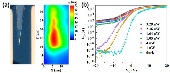
Figure 4.
Photoresponse of the phototransistor. (a) Spatial map of the photocurrent measured by conducting scan over the surface of the device using a focused laser beam at VDS = 5 V, VG = −10 V and incident power of 1.94 μW. (b) Ilight and Idark (IDS with and without illumination) measured under focused laser-beam irradiation for VDS = 5 V and VG = −20 to 20 V of 633 nm laser-beam illumination intensity from 1 nW to 3.28 µW.
To quantitatively assess the device’s photoresponse performance, two crucial parameters, photoresponsivity (R) and detectivity (D*), can be calculated according to the following formulas:
where Ilight is drain current, Idark is dark current and P is incident laser power.
where q is the element charge and A is the effective illuminated area. Figure 5a,b present photoresponsivity (R) and detectivity (D*) under the illumination of a 633 nm laser with different power intensities from 1 nW to 3.28 μW, respectively. As shown in Figure 5a, the photoresponsivity increases as gate voltage. The increasing gate voltage induces more electrons accumulated in the MoS2 channel. The photoresponse saturation emerges at VG of 20 V. A high responsivity of 1.28 × 10⁵ A·W−1 is shown at an illumination power of 1 nW, VG of 20 V and VDS of 5 V. As shown in Figure 5b, a high specific detectivity of ~7.17 × 10¹³ Jones is observed at an illumination power of 1 nW, VG of −5.5 V and VDS of 5 V, which are higher than the values reported in previous studies [1,2,5,6,8,28]. As shown in Figure 5c,d, the photocurrent (IPH = Ilight − Idark) and the logarithm of photoresponsivity of the device have a sublinear dependence on the logarithm of incident laser power from 1 nW to 3.28 μW, for VG of 20 V, VDS of 5 V. The photocurrent increases with laser power intensity, while photoresponsivity decreases with laser power intensity, which is similar to other 2D-based photodetectors [1,6,28,35].
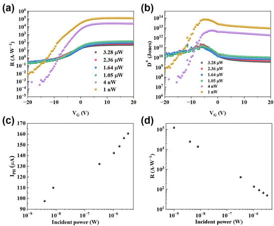
Figure 5.
Dependence of photoresponse on gate voltage and illumination intensity of the transistor. (a) Responsivity (R) and (b) detectivity (D*) of the device for VDS = 5 V, VG = −20 to 20 V, and 633 nm illumination intensity from 1 nW to 3.28 µW. (c) Photocurrent (IPH) and (d) photoresponsivity of the device as a function of the incident power for VDS = 5 V, VG = −20 to 20 V, and 633 nm illumination intensity from 1 nW to 3.28 µW.
In our work, the responsivity and specific detectivity of the device are much higher than those of conventional out-of-plane WSe2/MoS2 phototransistors [6], out-of-plane MoS2 p-n homojunctions [2], monolayer MoS2 phototransistors [28], multilayer MoS2 phototransistors [8] and laser-induced p-type doped WSe2 phototransistors [5] (Table 1). The responsivity and specific detectivity are approximately two orders higher than the out-of-plane WSe2/MoS2 phototransistor [6], demonstrating laser treatment attributes to enhancing photoproperties. The out-of-plane MoS2 p-n homojunction [2] has shown high photo responsivity and specific detectivity because they utilize a global illumination laser with a spot size of 2 mm, while we use a Raman laser spot (size of 1.04 µm) of Gaussian beam (NA = 0.5). Though they have approximately ten orders lower incident power intensity of 73 pW·cm−2 compared to ours of 1.13 × 10¹¹ pW·cm−2, we have higher responsivity, so we have better performance.

Table 1.
Performance comparison between phototransistors based on 2D-material semiconductors.
3.4. Time Dependence of Photoresponse
The time-dependent photoresponse was also measured to investigate the dynamic photoresponse of the device. A mechanical chopper and an oscilloscope (Agilent 86100A) were used to analyze the time-dependent photoresponse. Figure 6a,b present the time-dependent photoresponse of the device, which was measured using an optical chopper with a frequency of 1/30 Hz, incident power of 164 nW, at VG = −10 to 10 V with a step of 5 V and VDS = 5 V, respectively. The photocurrent of our device decreases as the time increases under positive gate voltage and increases as the time increases under negative gate voltage, which means our device can work in both bright and dark backgrounds. Figure 6c presents response time as a function of VG. Rise time decreases as VG increases. The occupied trap states in WSe2 increase as VG, leading to more photoelectrons participating in channel conductance.
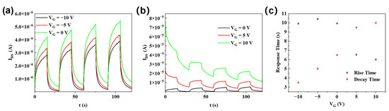
Figure 6.
Time-dependent photoresponse. (a) Time-dependent photoresponse of the phototransistor achieved using an optical chopper with a frequency of 1/30 Hz, for VG = −10 to 0 V, VDS = 5 V and incident power of 164 nW. (b) Time-dependent photoresponse of the device achieved using an optical chopper with a frequency of 1/30 Hz, for VG = 0 to 10 V, VDS = 5 V and incident power of 164 nW. (c) Response time as a function of VG.
3.5. Floating Gate and Photogating of Photoresponse
We further conducted IDS − VG transfer characteristics of forward sweep and backward sweep at 1 V/s of the device to investigate floating gate and photogating of the photoresponse. Figure 7a shows the IDS − VG transfer characteristics in dark conditions. Figure 7b shows the IDS − VG transfer characteristics under illumination intensity from 0.025 to 4 nW (power density of less than 1 nW was calculated from the transmittance of the filter). Figure 7c shows the IDS − VG transfer characteristics under illumination intensity from 2.14 to 4.48 µW. A clockwise hysteresis loop behavior was observed in both dark and illuminated conditions, indicating the charge trapping and de-trapping process at the interface between p-type doped WSe2 and MoS2. The trap charge density (Nt = 3.79 × 1012 cm−2) can be calculated using following formula:
where q is the element charge, ΔV = 16.1 V in Figure 7a is the maximum voltage shift between the transfer curves in the forward and backward sweeps and Cg = 3.77 × 10⁻⁸ F·cm−2 is the total capacitance of the 90 nm thick SiO2 layer and 5 nm WSe2 layer. The Nt is comparable with carrier density in MoS2 [36,37,38,39,40,41], which indicates that the trap states can substantially enhance the current under different illumination conditions [38,41]. Threshold voltage left-shift is observed in IDS − VDS transfer characteristics of forward sweep and backward sweep under increasing optical powers, which indicates that the trapping at the interface of p-doped WSe2 increases as illumination power, resulting in a photogating effect. Therefore, our device has high photoresponsivity and detectivity. In addition, our device can be used as optoelectronic memory for recording the perceived light information, benefiting from the large memory window.
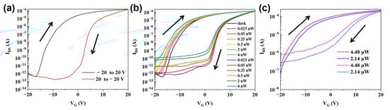
Figure 7.
IDS − VG transfer characteristics of forward sweep and backward sweep. (a) IDS − VG transfer characteristics for VDS = 5 V, VG = −20 to 20 V in dark conditions. (b) IDS − VG transfer characteristics for VDS = 5 V, VG = −20 to 20 V and 633 nm illumination intensity from 0.025 to 4 nW. (c) IDS − VG transfer characteristics for VDS = 5 V, VG = −20 to 20 V and 633 nm illumination intensity from 2.14 to 4.48 µW.
4. Conclusions
In this study, we developed an ultrasensitive phototransistor based on a laser-induced p-doped WSe2/MoS2 van der Waals heterojunction. A simple, efficient and selective p-doping approach was used for WSe2. The interface between p-doped WSe2 and MoS2 can separate the photogenerated electron–hole pairs and inject electrons into the MoS2 channel layer under laser illumination due to the strong built-in electric field. The p-doped WSe2/MoS2 heterojunction phototransistor shows a high photoresponsivity of ~1.28 × 10⁵ A·W−1 and a high specific detectivity of ~7.17 × 10¹³ Jones. Moreover, our phototransistor can operate in two modes. In the first mode, the photocurrent of our phototransistor decreases as the time increases under positive gate voltage, which means that our device can work in bright backgrounds. In the second mode, the photocurrent of our phototransistor increases as the time increases under negative gate voltage, indicating that our device can work in dark backgrounds. The capability of two work modes in our device indicates its potential application in bioinspired in-sensor visual adaptations [42]. By introducing trap states into the interface between p-doped WSe2 and MoS2, our device can be used for optoelectronic memory, benefiting from the large memory window. Together, these open a new avenue for future photoelectronic devices based on emerging 2D van der Waals heterojunctions with optimum device engineering.
Supplementary Materials
The following supporting information can be downloaded at: https://www.mdpi.com/article/10.3390/app13106024/s1, Figure S1: Operation principle schematic of photodetector; Figure S2: Preliminary experiment of laser-scanned process; Figure S3: Device fabrication process; Figure S4: Atomic force microscopy (AFM) characterization of the laser-scanned WSe2/MoS2 van der phototransistor; Figure S5: Corresponding fitting curves of Raman spectra (MoS2, WSe2 and laser-scanned WSe2/MoS2); Figure S6: PL spectra of WSe2/MoS2 heterojunction with undoped and doped regions; Figure S7: WSe2 FET before and after laser-scanned process; Figure S8: Spatial map of the photocurrent without bias; Table S1: Laser treatment parameters of the preliminary experiment.
Author Contributions
Conceptualization, J.Z., J.W. (Jing Wan), W.B, L.H., R.L., C.C. and Z.Q.; methodology, J.Z., X.Y., J.C. and J.W. (Jing Wang); software, J.W (Jing Wan)., W.B, L.H., R.L., C.C. and Z.Q.; validation, X.Y., J.C. and J.W. (Jing Wang); formal analysis, L.H., R.L., C.C. and Z.Q.; investigation, J.Z., X.Y. and J.C.; resources, W.B., C.C., and Z.Q.; data curation, J.W. (Jing Wan), W.B., R.L., L.H., C.C. and Z.Q.; writing—original draft preparation, J.Z., X.Y., J.C. and J.W (Jing Wang).; writing—review and editing, J.Z., J.W. (Jing Wan), W.B., L.H., R.L., C.C. and Z.Q.; visualization, J.W (Jing Wang).; supervision, L.H.; project administration, Z.Q.; funding acquisition, Z.Q. and C.C. All authors have read and agreed to the published version of the manuscript.
Funding
This research was funded by the Natural Science Foundation of China (nos. 62074045 and 61774040), the National Key R&D Program of China (grant no.2018YFA0703700), the Shanghai Municipal Natural Science Foundation (grant no. 20ZR1403200) and the National Young 1000 Talent Plan of China.
Institutional Review Board Statement
Not applicable.
Informed Consent Statement
Not applicable.
Data Availability Statement
The data presented in this study are available on request from the first author.
Conflicts of Interest
The authors declare no conflict of interest.
References
- Chen, Y.; Wang, Y.; Wang, Z.; Gu, Y.; Ye, Y.; Chai, X.; Ye, J.; Chen, Y.; Xie, R.; Zhou, Y.; et al. Unipolar barrier photodetectors based on van der Waals heterostructures. Nat. Electron. 2021, 4, 357–363. [Google Scholar] [CrossRef]
- Huo, N.; Konstantatos, G. Ultrasensitive all-2D MoS2 phototransistors enabled by an out-of-plane MoS2 PN homojunction. Nat. Commun. 2017, 8, 572. [Google Scholar] [CrossRef] [PubMed]
- Bansal, S.; Sharma, K.; Jain, P.; Sardana, N.; Kumar, S.; Gupta, N.; Singh, A.K. Bilayer graphene/HgCdTe based very long infrared photodetector with superior external quantum efficiency, responsivity, and detectivity. RSC Adv. 2018, 8, 39579–39592. [Google Scholar] [CrossRef] [PubMed]
- Bansal, S.; Singh, A.K.; Das, A.; Jain, P.; Prakash, K.; Sharma, K.; Kumar, N.; Sardana, N.; Gupta, N.; Kumar, S. Enhanced optoelectronic properties of bilayer graphene/HgCdTe-based single- and dual-junction photodetectors in long infrared regime. IEEE Trans. Nanotechnol. 2019, 18, 781–789. [Google Scholar] [CrossRef]
- Chen, J.; Wang, Q.; Sheng, Y.; Cao, G.; Yang, P.; Shan, Y.; Liao, F.; Muhammad, Z.; Bao, W.; Hu, L.; et al. High-performance WSe2 photodetector based on a laser-induced p-n junction. ACS Appl. Mater. Interf. 2019, 11, 43330–43336. [Google Scholar] [CrossRef]
- Shin, G.H.; Park, C.; Lee, K.J.; Jin, H.J.; Choi, S.Y. Ultrasensitive phototransistor based on WSe2-MoS2 van der Waals heterojunction. Nano Lett. 2020, 20, 5741–5748. [Google Scholar] [CrossRef]
- Fang, H.; Chuang, S.; Chang, T.C.; Takei, K.; Takahashi, T.; Javey, A. High-performance single layered WSe2 p-FETs with chemically doped contacts. Nano Lett. 2012, 12, 3788–3792. [Google Scholar] [CrossRef]
- Choi, W.; Cho, M.Y.; Konar, A.; Lee, J.H.; Cha, G.B.; Hong, S.C.; Kim, S.; Kim, J.; Jena, D.; Joo, J. High-detectivity multilayer MoS2 phototransistors with spectral response from ultraviolet to infrared. Adv. Mater. 2012, 24, 5832–5836. [Google Scholar] [CrossRef]
- Xiao, Y.; Qu, J.; Luo, Z.; Chen, Y.; Yang, X.; Zhang, D.; Li, H.; Zheng, B.; Yi, J.; Wu, R. Van der Waals epitaxial growth and optoelectronics of a vertical MoS2/WSe2 p–n junction. Front. Optoelectron. 2022, 15, 41. [Google Scholar] [CrossRef]
- Jeong, M.H.; Ra, H.S.; Lee, S.H.; Kwak, D.H.; Ahn, J.; Yun, W.S.; Lee, J.; Chae, W.S.; Hwang, D.K.; Lee, J.S. Multilayer WSe2/MoS2 heterojunction phototransistors through periodically arrayed nanopore structures for bandgap engineering. Adv. Mater. 2022, 34, 2108412. [Google Scholar] [CrossRef]
- Oh, G.H.; Kim, S.-i.; Kim, T. High-performance Te-doped p-type MoS2 transistor with high-K insulators. J. Alloys Compound. 2021, 860, 157901. [Google Scholar] [CrossRef]
- Zhang, R.; Drysdale, D.; Koutsos, V.; Cheung, R. Controlled layer thinning and p-type doping of WSe2 by vapor XeF2. Adv. Funct. Mater. 2017, 27, 1702455. [Google Scholar] [CrossRef]
- Ma, X.; Zhang, R.; An, C.; Wu, S.; Hu, X.; Liu, J. Efficient doping modulation of monolayer WS2 for optoelectronic applications. Chin. Phys. B 2019, 28, 037803. [Google Scholar] [CrossRef]
- Bie, Y.-Q.; Grosso, G.; Heuck, M.; Furchi, M.M.; Cao, Y.; Zheng, J.; Bunandar, D.; Navarro-Moratalla, E.; Zhou, L.; Efetov, D.K. A MoTe2-based light-emitting diode and photodetector for silicon photonic integrated circuits. Nat. Nanotechnol. 2017, 12, 1124–1129. [Google Scholar] [CrossRef] [PubMed]
- Wang, Q.; Chen, J.; Zhang, Y.; Hu, L.; Liu, R.; Cong, C.; Qiu, Z.-J. Precise layer control of MoTe2 by ozone treatment. Nanomaterials 2019, 9, 756. [Google Scholar] [CrossRef]
- Yang, S.; Lee, G.; Kim, J. Selective p-doping of 2D WSe2 via UV/ozone treatments and its application in field-effect transistors. ACS Appl. Mater. Interf. 2020, 13, 955–961. [Google Scholar] [CrossRef] [PubMed]
- Nipane, A.; Karmakar, D.; Kaushik, N.; Karande, S.; Lodha, S. Few-layer MoS2 p-type devices enabled by selective doping using low energy phosphorus implantation. ACS Nano 2016, 10, 2128–2137. [Google Scholar] [CrossRef] [PubMed]
- Kang, D.-H.; Hong, S.-T.; Oh, A.; Kim, S.-H.; Yu, H.-Y.; Park, J.-H. Nondegenerate n-type doping phenomenon on molybdenum disulfide (MoS2) by zinc oxide (ZnO). Mater. Res. Bullet. 2016, 82, 26–30. [Google Scholar] [CrossRef]
- Luo, T.; Pan, B.; Zhang, K.; Dong, Y.; Zou, C.; Gu, Z.; Zhang, L. Electron beam lithography induced doping in multilayer MoTe2. Appl. Surf. Sci. 2021, 540, 148276. [Google Scholar] [CrossRef]
- Wang, P.; Qu, J.; Wei, Y.; Shi, H.; Wang, J.; Sun, X.; Li, W.; Liu, W.; Gao, B. Spontaneous n-Doping in growing monolayer MoS2 by Alkali metal compound-promoted CVD. ACS Appl. Mater. Interf. 2021, 13, 58144–58151. [Google Scholar] [CrossRef]
- Khalil, H.M.; Khan, M.F.; Eom, J.; Noh, H. Highly stable and yunable chemical doping of multilayer WS2 field effect transistor: Reduction in contact resistance. ACS Appl. Mater. Interf. 2015, 7, 23589–23596. [Google Scholar] [CrossRef] [PubMed]
- Heo, K.; Jo, S.H.; Shim, J.; Kang, D.H.; Kim, J.H.; Park, J.H. Stable and reversible Triphenylphosphine-based n-type doping technique for molybdenum disulfide (MoS2). ACS Appl. Mater. Interf. 2018, 10, 32765–32772. [Google Scholar] [CrossRef] [PubMed]
- Kang, D.-H.; Kim, M.-S.; Shim, J.; Jeon, J.; Park, H.-Y.; Jung, W.-S.; Yu, H.-Y.; Pang, C.-H.; Lee, S.; Park, J.-H. High-performance transition metal dichalcogenide photodetectors enhanced by self-assembled monolayer doping. Adv. Funct. Mater. 2015, 25, 4219–4227. [Google Scholar] [CrossRef]
- Jo, S.H.; Kang, D.H.; Shim, J.; Jeon, J.; Jeon, M.H.; Yoo, G.; Kim, J.; Lee, J.; Yeom, G.Y.; Lee, S.; et al. A high-performance WSe2 /h-BN photodetector using a Triphenylphosphine (PPh3)-based n-doping technique. Adv. Mater. 2016, 28, 4824–4831. [Google Scholar] [CrossRef] [PubMed]
- Zhang, Q.; Ren, Z.; Wu, N.; Wang, W.; Gao, Y.; Zhang, Q.; Shi, J.; Zhuang, L.; Sun, X.; Fu, L. Nitrogen-doping induces tunable magnetism in ReS2. NPJ 2D Mater. Appl. 2018, 2, 22. [Google Scholar] [CrossRef]
- Chen, J.; Zhu, J.; Wang, Q.; Wan, J.; Liu, R. Homogeneous 2D MoTe2 CMOS inverters and p-n junctions formed by laser-irradiation-induced p-type doping. Small 2020, 16, e2001428. [Google Scholar] [CrossRef]
- Chen, J.; Shan, Y.; Wang, Q.; Zhu, J.; Liu, R. P-type laser-doped WSe2/MoTe2 van der Waals heterostructure photodetector. Nanotechnology 2020, 31, 295201. [Google Scholar] [CrossRef]
- Yin, Z.; Li, H.; Li, H.; Jiang, L.; Shi, Y.; Sun, Y.; Lu, G.; Zhang, Q.; Chen, X.; Zhang, H. Single-layer MoS2 phototransistors. ACS Nano 2012, 6, 74–80. [Google Scholar] [CrossRef]
- Mattmann, M.; Roman, C.; Helbling, T.; Bechstein, D.; Durrer, L.; Pohle, R.; Fleischer, M.; Hierold, C. Pulsed gate sweep strategies for hysteresis reduction in carbon nanotube transistors for low concentration NO2 gas detection. Nanotechnology 2010, 21, 185501. [Google Scholar] [CrossRef]
- Carrion, E.; Malik, A.; Behnam, A.; Islam, S.; Feng, X.; Pop, E. Pulsed nanosecond characterization of graphene transistors. In Proceedings of the 70th Device Research Conference, University Park, PA, USA, 18–20 June 2012; pp. 183–184. [Google Scholar] [CrossRef]
- Chen, J.; Zhu, J.; Li, P.; Wu, X.-M.; Liu, R.; Wan, J.; Ren, T.-L. Fabricating in-plane MoTe2 pn homojunction photodetector using laser-induced P-type doping. IEEE Trans. Electron Devices 2021, 68, 4485–4490. [Google Scholar] [CrossRef]
- Doan, M.-H.; Jin, Y.; Adhikari, S.; Lee, S.; Zhao, J.; Lim, S.C.; Lee, Y.H. Charge transport in MoS2/WSe2 van der Waals heterostructure with tunable inversion layer. ACS Nano 2017, 11, 3832–3840. [Google Scholar] [CrossRef] [PubMed]
- Fang, H.; Battaglia, C.; Carraro, C.; Nemsak, S.; Ozdol, B.; Kang, J.S.; Bechtel, H.A.; Desai, S.B.; Kronast, F.; Unal, A.A. Strong interlayer coupling in van der Waals heterostructures built from single-layer chalcogenides. Proc. Nat. Acad. Sci. USA 2014, 111, 6198–6202. [Google Scholar] [CrossRef] [PubMed]
- Cho, S.-Y.; Kim, S.J.; Lee, Y.; Kim, J.-S.; Jung, W.-B.; Yoo, H.-W.; Kim, J.; Jung, H.-T. Highly enhanced gas adsorption properties in vertically aligned MoS2 layers. ACS Nano 2015, 9, 9314–9321. [Google Scholar] [CrossRef] [PubMed]
- Deng, W.; You, C.; Chen, X.; Wang, Y.; Li, Y.; Feng, B.; Shi, K.; Chen, Y.; Sun, L.; Zhang, Y. High-performance photodiode based on atomically thin WSe2/MoS2 nanoscroll integration. Small 2019, 15, 1901544. [Google Scholar] [CrossRef]
- Park, Y.; Baac, H.W.; Heo, J.; Yoo, G. Thermally activated trap charges responsible for hysteresis in multilayer MoS2 field-effect transistors. Appl. Phys. Lett. 2016, 108, 83102. [Google Scholar] [CrossRef]
- Cai, Y.; Zhou, H.; Zhang, G.; Zhang, Y.-W. Modulating carrier density and transport properties of MoS2 by organic molecular doping and defect engineering. Chem. Mater. 2016, 28, 8611–8621. [Google Scholar] [CrossRef]
- Steinhoff, A.; Rosner, M.; Jahnke, F.; Wehling, T.O.; Gies, C. Influence of excited carriers on the optical and electronic properties of MoS2. Nano Lett. 2014, 14, 3743–3748. [Google Scholar] [CrossRef]
- Jiang, J.; Zou, X.; Lv, Y.; Liu, Y.; Xu, W.; Tao, Q.; Chai, Y.; Liao, L. Rational design of Al2O3/2D perovskite heterostructure dielectric for high performance MoS2 phototransistors. Nat. Commun. 2020, 11, 4266. [Google Scholar] [CrossRef]
- Kaushik, N.; Mackenzie, D.M.A.; Thakar, K.; Goyal, N.; Mukherjee, B.; Boggild, P.; Petersen, D.H.; Lodha, S. Reversible hysteresis inversion in MoS2 field effect transistors. NPJ 2D Mater. Appl. 2017, 1, 34. [Google Scholar] [CrossRef]
- Nur, R.; Tsuchiya, T.; Toprasertpong, K.; Terabe, K.; Takagi, S.; Takenaka, M. High responsivity in MoS2 phototransistors based on charge trapping HfO2 dielectrics. Commun. Mater. 2020, 1, 103. [Google Scholar] [CrossRef]
- Liao, F.; Zhou, Z.; Kim, B.J.; Chen, J.; Wang, J.; Wan, T.; Zhou, Y.; Hoang, A.T.; Wang, C.; Kang, J. Bioinspired in-sensor visual adaptation for accurate perception. Nat. Electron. 2022, 5, 84–91. [Google Scholar] [CrossRef]
Disclaimer/Publisher’s Note: The statements, opinions and data contained in all publications are solely those of the individual author(s) and contributor(s) and not of MDPI and/or the editor(s). MDPI and/or the editor(s) disclaim responsibility for any injury to people or property resulting from any ideas, methods, instructions or products referred to in the content. |
© 2023 by the authors. Licensee MDPI, Basel, Switzerland. This article is an open access article distributed under the terms and conditions of the Creative Commons Attribution (CC BY) license (https://creativecommons.org/licenses/by/4.0/).