Featured Application
This work investigates the potential application of microbiology and chemistry sensors and microfluidic devices.
Abstract
Surface acoustic wave (SAW) sensors have been applied in various areas with many advantages, such as their small size, high sensitivity and wireless and passive form. Love wave mode sensors, an important kind of SAW sensor, are mostly used in biology and chemistry monitoring, as they can be used in a liquid environment. Common Love wave mode sensors consist of a delay line with waveguide and sensitive layers. To extend the application of Love wave mode sensors, this article reports a novel Love wave mode sensor consisting of a waveguide layer with microphononic crystals (PnCs). To analyze the properties of the new structure, the band structure was calculated, and transmission was obtained by introducing delay line structures and quasi-three-dimensional models. Furthermore, devices with a traditional structure and novel structure were fabricated. The results show that, by introducing the designed microstructure of phononic crystals in the waveguide layer, the attenuation was barely increased, and the frequency was shifted by a small amount. In the liquid environmental experiments, the novel structure with micro PnCs shows even better character than the traditional one. Moreover, the introduced microstructure can be extended to microreaction tanks for microcontrol. Therefore, this novel Love wave mode sensor is a promising application for combining acoustic sensors and microfluidics.
1. Introduction
Surface acoustic wave (SAW) sensors, with their many advantages of small size, high sensitivity and wireless and passive form, have been applied in many areas of radar, television, phone and microelectromechanical systems (MEMS). Common types of SAW waves include the Rayleigh wave [1], shear horizontal wave [2], Love wave [3] and Lamb wave [4]. Rayleigh wave propagating in the surface of the piezoelectric is the earliest mode to be studied and widely used in the remote sensors of temperature and strain with high Q and low attenuation. However, when it is used in the liquid, it will have a serious loss of acoustic energy, as it has a large vertical displacement component. Different to the Rayleigh wave, the energy of the Love wave is focused on the waveguide layer and can propagate in the liquid; thus, the Love wave mode sensor can be used in the area of biochemistry [5,6,7].
Love wave mode is a kind of horizontal shear wave, of which the particle vibrates perpendicularly to the direction of propagation and the direction of the surface normal. The energy of the wave is trapped in the thin waveguide layer without radiating into a semi-infinite medium [8,9]. The Love wave is sensitive to surface disturbance, and thus, it has application potential in a liquid environment due to its only shear displacement parallel to the substrate.
The common Love wave mode sensor consists of a delay line structure with an emission transducer, receiving transducer, waveguide layer and sensitive layer [10], as shown in Figure 1. Usually, the wave in the piezoelectric wafer propagates perpendicularly to the transducers. When it approaches the waveguide layer, which has lower shear wave velocity, the Love wave mode will be excited with the vibration perpendicular to both the direction of wave propagation and the normal direction of the surface. When there are different target liquids (such as different concentrations and different permittivity) on the surface of the waveguide layer, the velocity of the Love wave mode will be changed. Thus, the detection signal will have different characteristics, which can represent different target liquids. Through the principle of the Love wave mode sensor, it can be observed that the performance of the Love wave mode sensor will be significantly influenced by the waveguide layer.
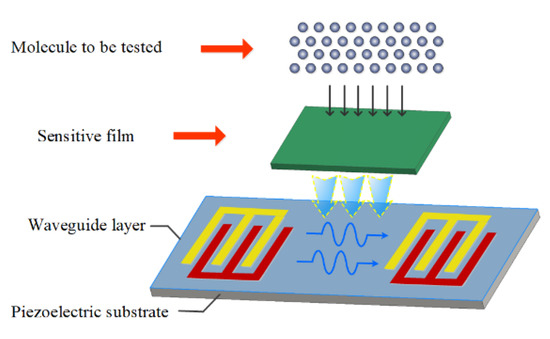
Figure 1.
Schematic diagram of the Love wave mode sensor.
Much research has been conducted on the waveguide layer materials [11,12,13,14,15,16,17,18]. The ideal waveguide layer material should have low shear velocity, low density and also excellent elastic characteristics and low acoustic absorption; otherwise, it will lead to a large insertion loss, causing a large amount of noise. Thus, much research focuses on the waveguide layer materials with excellent uniformity, high density, high density, high surface flatness and low stress to improve the performance of devices. The employed waveguide layer materials include organic waveguide, inorganic waveguide, composite waveguide and gradient waveguide, such as SiO2 [11,12], ZnO [13,14,15], PMMA [16] and SU8 [17,18].
On the other hand, piezoelectric phononic crystals (PnCs) [19] are periodic elastic structures consisting of two different elastic materials, which have band gaps. This property has led to many explorations regarding the use of piezoelectric PnCs in SAW devices [20,21,22,23,24,25]. These application explorations include SAW waveguides studied by T.T. Wu in 2006 and Yahui Tian in 2014, and SAW resonators studied by Solal in 2010. They demonstrate the potential for using piezoelectric PnCs in SAW devices to improve their characters. However, most prior studies have focused on the Rayleigh wave devices.
As the developing on-chip micro–nanosystems need many microstructures to achieve microchannels and microcontrol [26,27,28], to promote on-chip micro–nanosystems combined with Love wave mode sensors, this paper proposed a new Love wave mode delay line waveguide layer structure with microphononic crystals, which can be extended to be used as microchannels. As micro-PnCs consist of pillars on the waveguide layer, the most important factor is to analyze the propagation property of the Love wave and design to avoid disturbing the attenuation.
To analyze the Love wave property in the delay line waveguide layer with microphononic crystals, eigen modes and transmission parameters were analyzed. To verify the reliability of the theory, experiments with and without liquid environment were carried out.
2. Materials and Methods
The delay line waveguide layer with microphononic crystals consists of periodic micropillars embedded in the origin waveguide layer. To establish the theoretical platform for analysis, this study used the periodic micro-Al pillars in the SiO2 waveguide layer as an example to analyze the eigen modes and transmission parameter.
The structure is shown in Figure 2; the Al pillars have a length of 20 um, and the side length on the top surface is 10 um. The waveguide layer is SiO2 and the substrate is 36° LiTaO3.
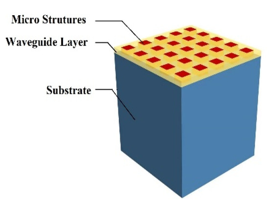
Figure 2.
Schematic diagram of a Love wave mode waveguide layer with microphononic crystals.
To analyze the Love wave property in the delay line waveguide layer with microphononic crystals, eigen modes and transmission parameters were analyzed, respectively. In the eigen mode analysis, a single-cell model was adopted with the finite element method (FEM), and in the transmission parameters analysis, two delay line structures and quasi-three-dimensional models were introduced.
2.1. Eigen Mode Analysis
For the ideal two-dimensional piezoelectric PnCs, according to the Bloch periodic theorem, it can be simplified into the single-cell model, as shown in Figure 3a. For the calculation of eigen modes, the calculated wave vector can be limited in its first Brillouin region (as shown in Figure 3b) for discrete scanning.
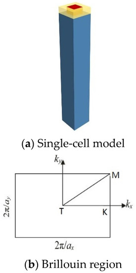
Figure 3.
Single-cell model and Brillouin region.
The finite element method was used to analyze the energy band structure, namely, the eigenvalue character. The simplified model was adopted, and a single cell was extracted as the PnC period, as shown in Figure 3a. In the model, periodic boundary conditions (PBC) were adopted on both sides of the X and Y directions, and a perfect matching layer (PML) was adopted on the bottom as an absorptive boundary. Between the two materials, a continuum boundary was used on their edges; namely, the stress, displacement and potential are continuous.
In the piezoelectric substrate, the relationships, strain vs. stress and displacement vs. electric field are considered linear; thus, the coupled constitutive equations in piezoelectric substrate can be expressed as follows:
where and are the stress and strain tensors, respectively. , and are the stiffness constant, piezoelectric stress constant and dielectric permittivity constant, respectively. and are the electric displacement vector and electric field, respectively.
According to the energy band theory, ideal PnCs have discrete translational periodicity, thus satisfying the Bloch theorem of the space periodic system; that is, the field component can be expressed as follows:
where represents all displacement components and the electric potential, and the Bloch wave vector is the wave vector in the first Brillouin region. The problem of the eigen field analysis of an ideal phononic crystal with infinite periods is in fact the problem in determining the given wave vector and corresponding eigen modes.
The discrete eigenvalue solution equation can be expressed as follows:
For Equation (4), the finite element method was used to scan different wave vectors by parameterization (discrete wave vectors on the three edges of the first Brillouin) to solve the eigenvalue. Therefore, the band structure and mode property of the mixed modes in two-dimensional piezoelectric phononic crystals can be obtained.
With the above method, in this paper, the eigen modes of Al/SiO2/36° LiTaO3 phononic crystals were analyzed. Figure 4 illustrates the band structure and typical mode of the PnCs. Multiple curves consisted of discrete points for eigen frequencies at each wave vector. The X-axis is the wave vector scanning the area of the first Brillouin region, which can be on behalf of the whole band structure according to the Bloch Periodic Theorem. The Y-axis is the eigen frequencies for each wave vector. The results show that in the low-frequency stage below 200 MHz, there is nearly no band gap. This means that most of the wave can be transmitted in this region with little attenuation.
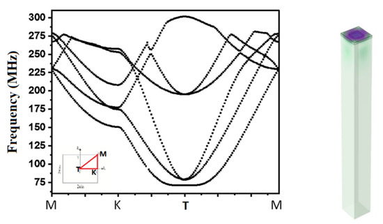
Figure 4.
Band structure of Al/SiO2/36° LiTaO3 and the typical eigen mode.
2.2. Transmission Parameters Analysis
To further analyze the Love wave transmission in the new waveguide layer with micro PnCs, transmission parameters were analyzed. As the Love wave is a typical three-dimensional wave, its analysis cannot be simplified into a two-dimensional model as with the Rayleigh wave. Therefore, to reduce the calculation complexity, quasi-three-dimensional models were adopted. To guarantee that the excited wave had a Love wave mode, structures of the delay line in the theory were introduced in this paper according to the authors in [25].
The Love wave mode delay lines, as shown in Figure 5, consist of an emitting interdigital transducer (IDT), a receiving IDT and the transmitting path with or without Al/SiO2/36° LiTaO3 piezoelectric PnCs, respectively. Quasi-three-dimensional models were applied to each to calculate their Y parameters.
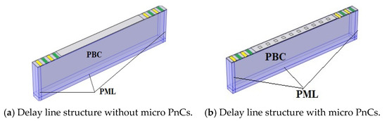
Figure 5.
The quasi-three-dimensional models of delay line structures with and without micro PnCs.
In the models, one row was extracted in the direction parallel to the IDT and the periodic boundary condition was adopted in this direction. Perpendicular to the IDT, there were two pairs of the transmitting and receiving IDT and 10 periods of pillars on the transmission path. On both sides of the edge of the transmission path, PML was adopted. On the bottom of the models, PML was also used to suppress the strong reflection of the boundary.
With the models above, FEM in frequency domain analysis, combined with the electric terminals applying on the IDT, was used to calculate the Y parameters of both delay line structures. In the model, transmitting IDT was set as terminal 1 and ground, and receiving IDT was set as terminal 2 and ground. For terminal 1, 1 V voltage was applied. With the algorithm in the FEM software, the Y parameters can be derived. The results of the Y parameters are as shown in Figure 6.
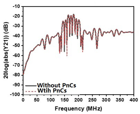
Figure 6.
Transmission of the Love wave mode delay line.
Furthermore, to analyze the transmission of the piezoelectric PnCs, a P matrix as shown in Figure 7 was introduced. According to the theory of the P matrix [29], IDT can be described as a three-port network (Figure 4) with two acoustical ports and one electrical port, as shown in the following equation:
where is the input of the acoustical ports, is the output of the acoustical ports, u is the voltage of the electrical port, i is the electrical current of the electrical port and is the P matrix element of the IDTs.
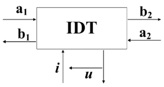
Figure 7.
The P matrix model of an IDT.
Differing from IDT, the P matrices of the free waveguide layer and waveguide layer with micro piezoelectric PnCs transmitting paths can be reduced to two acoustical ports, as shown in the following equation:
Based on the P matrices of IDT and transmitting paths, the equivalent models of the two SAW delay lines can be derived as shown in Figure 8. We assume that the arrangement of delay line structures is perfectly symmetric and the emitting IDT and the receiving IDT are the same. Thus, the P matrices of these IDTs are the same.
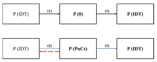
Figure 8.
The P matrix equivalent models of delay line structures with and without micro PnCs.
In Figure 8, transmitting path ① indicates that the signal transmits from the emitting IDT to the receiving IDT across the free surface, which can be expressed by the following Equation:
where is the first signal in the transfer admittance of the Love wave mode delay line with the common waveguide layer transmitting path and is the transmission coefficient of the common waveguide layer transmitting path.
In transmitting path ②, the signal transmits from the emitting IDT to the receiving IDT across the 2D piezoelectric PnCs, yielding the following equation:
where is the first signal in the transfer admittance of the Love wave mode delay line with the piezoelectric PnCs, and is the transmission coefficient of the piezoelectric PnCs.
In transmitting path ③, the signal is sent from the emitting IDT, reflected by the piezoelectric PnCs and received by the emitting IDT. Thus, the P matrix provides the relationship shown in the following equation:
where is the reflected signal of PnCs in the input admittance of the Love wave mode delay line with the piezoelectric PnCs, and is the reflection of the piezoelectric PnCs.
By comparing transmitting path ① and transmitting path ② with Equations (7) and (8), the transmission coefficient of the piezoelectric PnCs can be obtained via Equation (10) when is not equal to zero:
In this way, the transmission of the piezoelectric PnCs was obtained as shown in Figure 9. The results in the valid region [0,1] are valid; beyond this area, the results show errors caused by the numerical calculation for these two models.
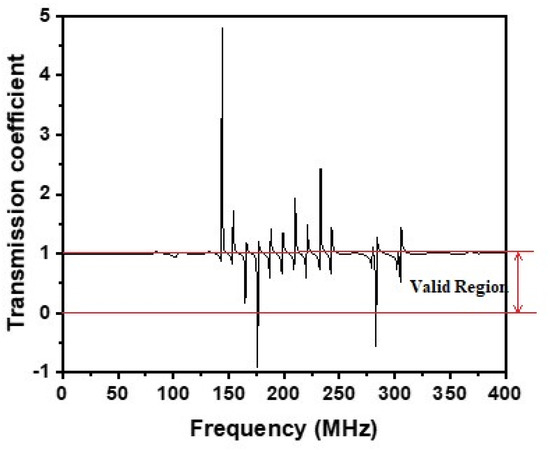
Figure 9.
The transmission of micro PnCs.
3. Experiments and Results
3.1. Fabrication of Devices and Experimental Setup
Microelectromechanical system (MEMS) fabrication technology was used in this paper to produce a new Love wave mode delay line structure with a waveguide layer of micro PnCs. The fabrication process included three layers: Al IDT and PnCs pillars, a SiO2 layer and an Au-sensitive film layer. For the process, cleaning, coating films, photoetching and etching were conducted in stages.
The first Al layer and the third Au layer were fabricated by employing magnetron sputtering. The second SiO2 layer was fabricated using plasma-enhanced vapor deposition.
As shown in Figure 10, the fabricated structure has the dimensions of 4 mm × 2 mm × 0.5 mm. In the actual devices, there are 90 pairs of IDTs and 250 × 250 arrays in the waveguide layer. Photos of microstructures were taken by the Leica 3-D confocal microscope, as shown in the Figure 10b–d, including the surface structures and body structures.
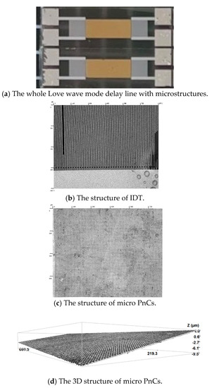
Figure 10.
Devices of the Love wave mode delay line and microstructure.
The electrical responses were measured by the vector network analyzer (VNA) with the Keysight E5071C. As the direct measurement data had many reflective signals of the bottom, the time domain window was added to extract the useful information. The treated results are demonstrated in Figure 11. From the Figure 11, it can be seen that the main peak has been slant after introducing the micro PnCs, along with a little shift up of the frequency, but with little attenuation.
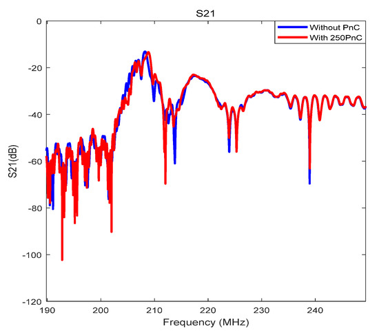
Figure 11.
Responses of fabricated Love wave mode delay lines.
3.2. Liquid Environmental Experiment
To further explore the actual performance of the new Love wave mode delay line structure with micro piezoelectric PnCs, experiments with liquid environment were conducted. As shown in Figure 12, the micro liquid channel was designed for the device using polydimethylsiloxane (PDMS), which has good biocompatibility. Using the technology of the boning, the micro-PDMS channel was combined with the Love wave mode sensor chip.
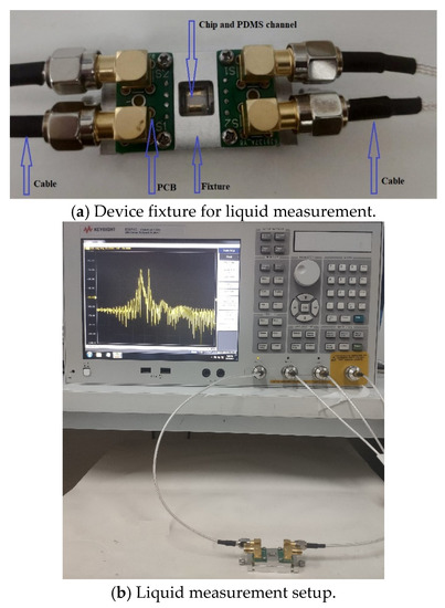
Figure 12.
Liquid environmental experiment.
For the liquid environmental experiment, phosphate buffer saline (PBS) was used as the liquid sample. Devices with the traditional Love wave mode delay line structure and the new Love wave mode delay line structure were added, respectively, with 2 µL, 5 µL and 10 µL PBS solution. The electrical responses were also measured using the vector network analyzer. The treated results of the Love wave mode delay lines with respective original status, adding PDMS channel, and adding PBS solution, are demonstrated in Figure 13.
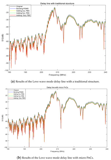
Figure 13.
Liquid environmental experimental results of the Love wave mode delay line.
The experimental results show that, for the Love wave mode delay line structures, when PDMS was boned on the device, about 1 dB of attenuation was introduced for both the traditional structure and micro PnCs. From Table 1, it can be seen when 2 µL PBS was added, the frequency shift of Love wave mode delay line was about 32 KHz and 39 KHz, respectively, with the traditional structure and micro PnCs. When 5 µL PBS was added, the frequency shift of Love wave mode delay line was about 76 KHz and 87 KHz, respectively, with the traditional structure and micro PnCs. Thus, it has been proven that the new novel structure with micro PnCs can be applied in liquid environments as well as the traditional structure, and even obtains better results. Furthermore, this micro PnCs structure can be extended to microreaction tanks for microcontrol. Therefore, this new device structure has a promising application for combining acoustic sensors and microfluidics.

Table 1.
Center frequency of the delay line (MHz).
4. Conclusions
Love wave mode sensors show great potential in MEMS for physical, chemical and biological monitoring, with their unique small sizes and wireless features. To extend the application of Love wave mode sensors, this paper proposed a novel structure of a waveguide layer in the delay line with microphononic crystals. Through the analysis of the band structures of the piezoelectric phononic crystals, the band pass was found. Therefore, the specific PnCs were introduced in the Love wave mode delay line waveguide layer. To effectively analyze the propagation of the Love wave mode sensor in the novel structure, two delay lines and quasi-three-dimensional models were introduced to calculate the responses of the Love wave. From the analysis of the results, it can be seen that, with the specific microphononic crystals, the propagation attenuation of the Love wave can barely be increased. Furthermore, experiments verify the results that the introduction of micro PnCs does not cause a serious disturbance in attenuation. Additionally, liquid environmental experiments were conducted to verify its viability.
As this microstructure can be extended to microreaction tanks for microcontrol, this novel Love wave mode sensor with a specific design has a promising application for combining acoustic sensors and microfluidics. Therefore, in future work, the application of this new structure can be further studied.
Author Contributions
Conceptualization, Y.T. and H.L.; methodology, Y.T.; software, L.W.; validation, Y.T.; formal analysis, W.L.; investigation, Y.T.; resources, H.L.; data curation, W.C.; writing—original draft preparation, Y.T.; writing—review and editing, Z.L. and X.M.; visualization, L.W.; supervision, H.L.; project administration, X.M.; funding acquisition, H.L. All authors have read and agreed to the published version of the manuscript.
Funding
This work was partially supported by the National Natural Science Foundation of China (12004413). Additional support was provided by the Key Research Project of Guangdong Province (2020B0101040002), the Technology Innovation 2025 Program of the Municipality of Ningbo (2019B10122), the Research and Development Program in Key Disciplines of Hunan Province (2019GK2111), the Technology Nova Program of Beijing (Z201100006820012) and the Tianjin Enterprise Science and Technology Commissioner Project (19JCTPJC56200).
Informed Consent Statement
Not applicable.
Data Availability Statement
Not applicable.
Conflicts of Interest
The authors declare no conflict of interest.
References
- Wu, S.; Lin, Z.-X.; Ro, R.; Lee, M.-S. Rayleigh and shear horizontal surface acoustic properties of (100) ZnO films on silicon. IEEE Trans. Ultrason. Ferroelectr. Freq. Control. 2010, 57, 1237–1239. [Google Scholar] [CrossRef]
- Ro, R.; Lee, R.; Lin, Z.-X.; Sung, C.-C.; Chiang, Y.-F.; Wu, S. Surface acoustic wave characteristics of a (100) ZnO/(100) AlN/diamond structure. Thin Solid Film. 2013, 529, 470–474. [Google Scholar] [CrossRef]
- Länge, K.; Rapp, B.; Rapp, M. Surface acoustic wave biosensors: A review. Anal. Bioanal. Chem. 2008, 391, 1509–1519. [Google Scholar] [CrossRef] [PubMed]
- Yongha, S.; Songbin, G. Wideband RF filters using medium-scale integration of Lithium Niobate laterally vibrating resonators. IEEE Electron Device Lett. 2017, 38, 387–390. [Google Scholar]
- Du, J.; Harding, G.L.; Collings, A.F.; Dencher, P.R. An experimental study of Love-wave acoustic sensors operating in Liquids. Sens. Actuators A 1997, 60, 54–61. [Google Scholar] [CrossRef]
- Harding, G.L.; Du, J.; Dencher, P.R.; Barnett, D.; Howe, E. Love wave acoustic immunosensor operating in liquid. Sens. Actuators A 1997, 61, 279–286. [Google Scholar] [CrossRef]
- Gizeli, E.; Goddard, N.J.; Lowe, C.R.; Stevenson, A.C. A Love plate biosensor utilizing a polymer layer. Sens. Actuators B 1992, 6, 131–137. [Google Scholar] [CrossRef]
- Oh, H.; Wang, W.; Lee, K.; Yang, S. Development of wireless Love wave biosensor on 41°YXLiNbO3. Smart Mater. Struct. 2009, 18, 1–9. [Google Scholar] [CrossRef] [Green Version]
- Oh, H.; Wang, W.; Lee, K.; Yoon, H.C.; Yang, S. Wirelessly driven and battery-free Love wave biosensor based on DNP immobilization. Jpn. J. Appl. Phys. 2009, 48, 06FJ0-1-7. [Google Scholar] [CrossRef]
- Mitsakakis, K.; Tserepi, A.; Gizeli, E. Integration of microfluidics with a love wave sensor for the fabrication of a multisample analytical mi-crodevice. J. Microelectromechanical Syst. 2008, 17, 1010–1019. [Google Scholar] [CrossRef]
- Kovacs, G.; Vellekoop, M.; Haueis, R.; Lubking, G.; Venema, A. A love wave sensor for (bio)chemical sensing in liquids. Sensors Actuators A Phys. 1994, 43, 38–43. [Google Scholar] [CrossRef]
- Talbi, A.; Soltani, A.; Rumeau, A.; Taylor, A.; Drbohlavova, L.; Klimša, L.; Kopeček, J.; Fekete, L.; Krecmarova, M.; Mortet, V. Simulations, fabrication, and characterization of diamond-coated Love wave-type surface acoustic wave sensors. Phys. Status Solidi A 2015, 212, 2606–2610. [Google Scholar] [CrossRef]
- Cinzia, C.; Muhanmmad, H. A theoretical study of Love wave sensors based on ZnO-Glass layered structures for application to liquid envi-ronment. Biosensors 2016, 6, 59. [Google Scholar]
- Chu, S.-Y.; Water, W.; Liaw, J.-T. An investigation of the dependence of ZnO film on the sensitivity of Love mode sensor in ZnO/quartz structure. Ultrasonics 2002, 41, 133–139. [Google Scholar] [CrossRef]
- Panth, M.; Cook, B.; Zhang, Y.; Ewing, D.; Tramble, A.; Wilson, A.; Wu, J. High-Performance Strain Sensors Based on Vertically Aligned Piezoelectric Zinc Oxide Nanowire Array/Graphene Nanohybrids. ACS Appl. Nano Mater. 2020, 3, 6711–6718. [Google Scholar] [CrossRef]
- Du, J.; Harding, G.; Ogilvy, J.; Dencher, P.; Lake, M. A study of Love-wave acoustic sensors. Sens. Actuators A Phys. 1996, 56, 211–219. [Google Scholar] [CrossRef]
- Palfreyman, J.; Love, D.; Philpott, A.; Vyas, K.; Cimorra, C.; Mitrelias, T.; Barnes, C.; Muir, L.; Cook, G.; Keynes, R. Hetero-Coated Magnetic Microcarriers for Point-Of-Care Diagnostics. IEEE Trans. Magn. 2012, 49, 285–295. [Google Scholar] [CrossRef]
- Francis, L.A.; Friedt, J.M.; Bartic, C.; Campitelli, A. An SU-8 liquid cell for surface acoustic wave biosensors. Proc. SPIE Int. Soc. Opt. Eng. 2004, 5455, 353–363. [Google Scholar]
- Sigalas, M.; Economou, E. Elastic and acoustic wave band structure. J. Sound Vib. 1992, 158, 377–382. [Google Scholar] [CrossRef]
- Sun, J.H.; Wu, T.T. Guided surface acoustic waves in phononic crystal waveguides. In Proceedings of the 2006 IEEE Ultrasonics Symposium, Vancouver, BC, Canada, 3–6 October 2006; pp. 673–676. [Google Scholar]
- Yoon, J.; Mayer, M.; Ebner, T.; Wagner, K.; Wixforth, A. Advanced 2D periodic array and full transversal mode suppression. In Proceedings of the IEEE 2013 Joint UFFC, EFTF and PFM Symposium, Prague, Czech Republic, 21–25 July 2013; pp. 733–736. [Google Scholar] [CrossRef]
- Yahui, T.; Honglang, L.; Wenjia, T.; Yabing, K.; Jingling, C.H.; Shitang, H. A weighted waveguide for surface acoustic waves based on two-dimensional piezoelectric phononic crystals. In Proceedings of the 2014 IEEE Symposium on Piezoelectricity, Acoustic Waves, and Device Applications (SPAWDA), Beijing, China, 30 October–2 November 2014; pp. 375–378. [Google Scholar]
- Solal, M.; Gratier, J.; Kook, T. A SAW resonator with two-dimensional reflectors. IEEE Trans. Ultrason. Ferroelectr. Freq. Control. 2010, 57, 30–35. [Google Scholar] [CrossRef]
- Yudistira, D.; Boes, A.; Djafari-Rouhani, B.; Pennec, Y.; Yeo, L.; Mitchell, A.; Friend, J.R. Monolithic Phononic Crystals with a Surface Acoustic Band Gap from Surface Phonon-Polariton Coupling. Phys. Rev. Lett. 2014, 113, 215503. [Google Scholar] [CrossRef] [Green Version]
- Yahui, T.; Honglang, L.; Yabing, K.; Ce, Y.; Shitang, H. P-Matrix analysis of surface acoustic waves in piezoelectric phononic crystals. Trans. Ultrason. Ferroelectr. Freq. Control. 2016, 63, 757–763. [Google Scholar]
- Juarez-Martinez, G.; Chiolerio, A.; Allia, P.; Poggio, M.; Degen, C.L.; Zhang, L.; Nelson, B.J.; Dong, L.; Iwamoto, M.; Buehler, M.J.; et al. Microfludic Whole-Cell Biosensor. In Encyclopedia of Nanotechnology; Springer: Dordrecht, The Netherlands, 2012; pp. 1415–1419. [Google Scholar] [CrossRef]
- Yamanishi, Y.; Feng, L.; Arai, F. On-Demand and size-controlled production of emulsion droplet in microfludic devices. In Proceedings of the 2010 IEEE 23rd International Conference on Micro Electro Mechanical Systems (MEMS), Hong Kong, China, 24–28 January 2010; pp. 1087–1090. [Google Scholar] [CrossRef]
- Bui, T.H.; Duc, T.B.; Duc, T.C. Microfluidic injector simulation with fsaw sensor for 3-D integration. IEEE Trans. Instrum. Meas. 2015, 64, 849–856. [Google Scholar]
- Tobolka, G. Mixed Matrix Representation of SAW Transducers. IEEE Trans. Sonics Ultrason. 1979, 26, 426–427. [Google Scholar] [CrossRef]
Publisher’s Note: MDPI stays neutral with regard to jurisdictional claims in published maps and institutional affiliations. |
© 2021 by the authors. Licensee MDPI, Basel, Switzerland. This article is an open access article distributed under the terms and conditions of the Creative Commons Attribution (CC BY) license (https://creativecommons.org/licenses/by/4.0/).