Review

Copper Nanowires for Transparent Electrodes: Properties, Challenges and Applications

by
Vittorio Scardaci
Dipartimento di Scienze Chimiche, Università degli Studi di Catania, Viale A. Doria 6, 95125 Catania, Italy
Appl. Sci. 2021, 11(17), 8035; https://doi.org/10.3390/app11178035
Submission received: 12 August 2021 / Revised: 24 August 2021 / Accepted: 26 August 2021 / Published: 30 August 2021
(This article belongs to the Special Issue Advances in Nanomaterials Based Transparent Conductors)

Abstract

:
Transparent electrodes are essential elements of devices bearing a screen or display, as well as solar cells, LEDs etc. To overcome the drawbacks presented by indium tin oxide, nanomaterials have been proposed for a long time as alternatives. Metal nanowires are particularly interesting for their high intrinsic electrical conductivity. Copper nanowires have attracted wide interest due to the low cost and high abundancy of the starting material. However, they are easily oxidized thus suitable strategies must be devised to prevent it. This review discusses the fundamental properties and challenges of copper nanowires, focusing on the efforts made to make them longer and thinner then the strategies to prevent oxidation and to join them in the network are presented. After that, mechanical properties are summarized and applications are presented, before conclusions and perspectives are finally given.

1. Introduction

Transparent conductors are key components of a wide range of devices that are common in everyday use. Such devices include displays, touch screens, light-emitting diodes (LEDs), solar cells, memory devices, to name a few [1]. While commercial devices employ indium tin oxide (ITO) as transparent conductor, this material is far from ideal due to the toxicity of indium and its availability issues that eventually will drive the cost up. Moreover, the expanding technological interest in flexible electronics rules out ITO due to its intrinsic brittleness, which would bring the material to failure over bending [2,3]. The last two decades have thus seen significant research and development effort from both the scientific community and the industry to find suitable alternatives.
In order to serve as transparent conductor, a material should have the lowest possible sheet resistance, Rs, associated with the highest possible transmittance, T, usually measured and reported at 550 nm. To match ITO performance a transparent conductor should have Rs < 100/Ω/sq and T > 90% [4]. Carbon nanotubes have been initially proposed as alternatives, as they ensure high conductivity and transparency [5,6,7,8]. However, their performance never reached that of ITO. After the discovery of graphene, this has also been proposed as ITO alternative, which only matched, and surpassed, ITO performance when grown as a single large area graphene sheet [9], while sheets produced by liquid phase exfoliation showed lesser performance than carbon nanotubes [10,11,12].
Silver nanowires (NWs) were proposed as an exciting ITO alternative given their high conductivity due to the metallic character. Indeed, Ag NWs were able to match ITO performance both in terms of Rs and T [13,14,15,16]. However, Ag is also expensive and not very abundant [17], thus NWs made of other metals have been pursued. For example copper (Cu) has been proposed as an alternative being almost as conductive as Ag and at the same time much cheaper and more abundant [17]. Indeed, the pioneering work by Rathmell et al. paved the way for the utilization of Cu NWs as ITO alternatives [18,19,20]. Cu NWs however suffer from the issues common to Cu in general, i.e., the presence of a native oxide as well as oxidation over time under ambient conditions, which hinder the conductivity and the stability. Common methods, like annealing, were proposed but had low compatibility with processing, for example in flexible electronics.
While other reviews have been published on the topic of Cu NW based transparent electrodes [21,22], Ref [21] while quite comprehensive is already five years old and Ref. [22] only focusses on applications. While the Cu NW synthesis is not the main scope of this review, synthetic strategies used for the fabrication of transparent conductors, especially those presenting an advantage in terms of electrical and optical properties will be briefly covered. More comprehensive reviews on the synthesis of Cu NWs can be found in Refs. [23,24]. This paper aims at giving a comprehensive overview on the topic including the most recent results, and is structured as follows:

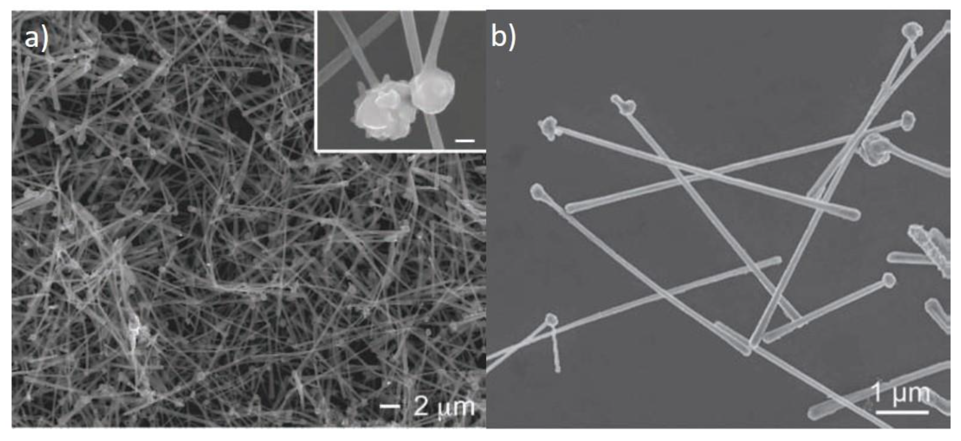
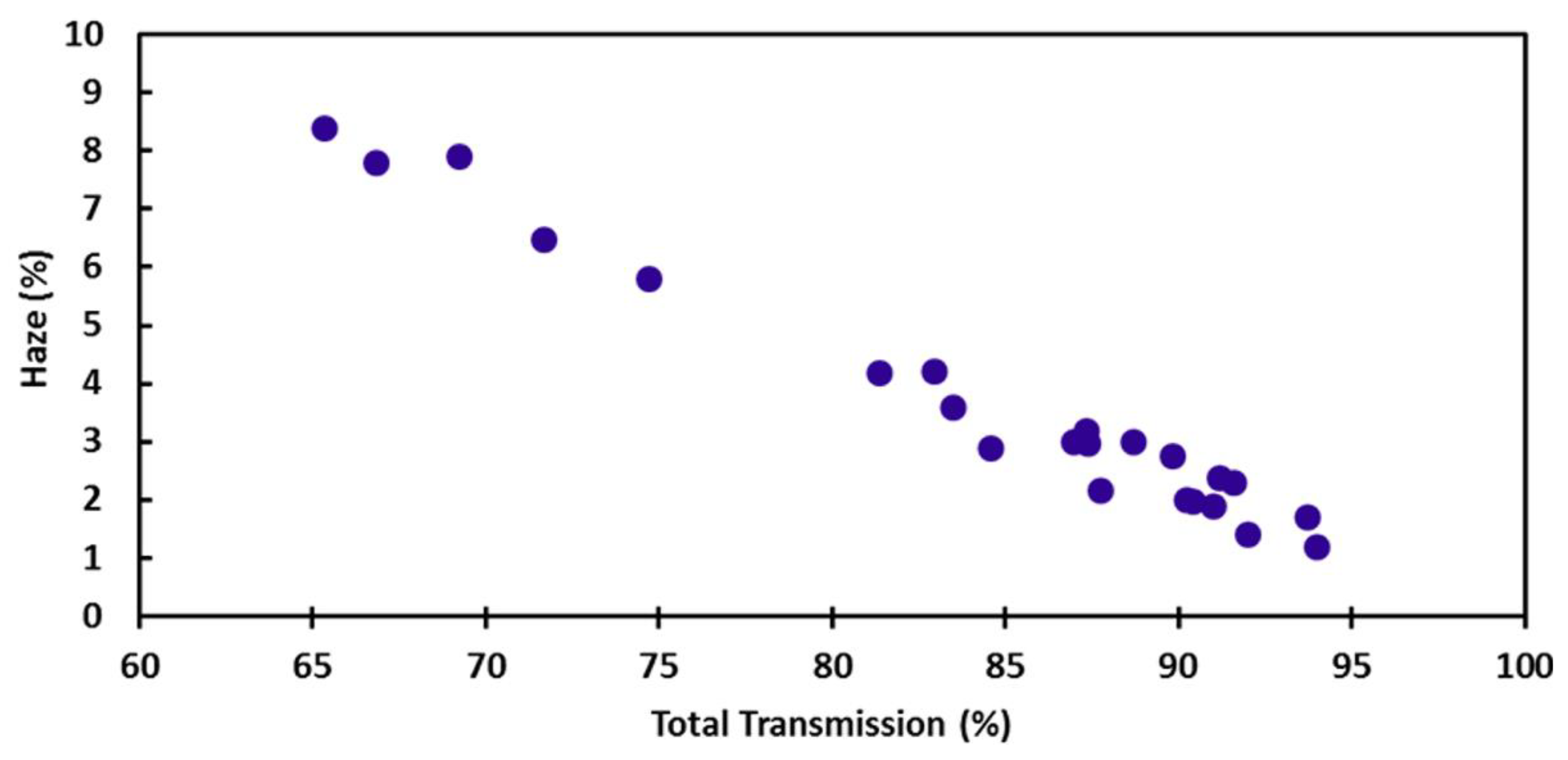
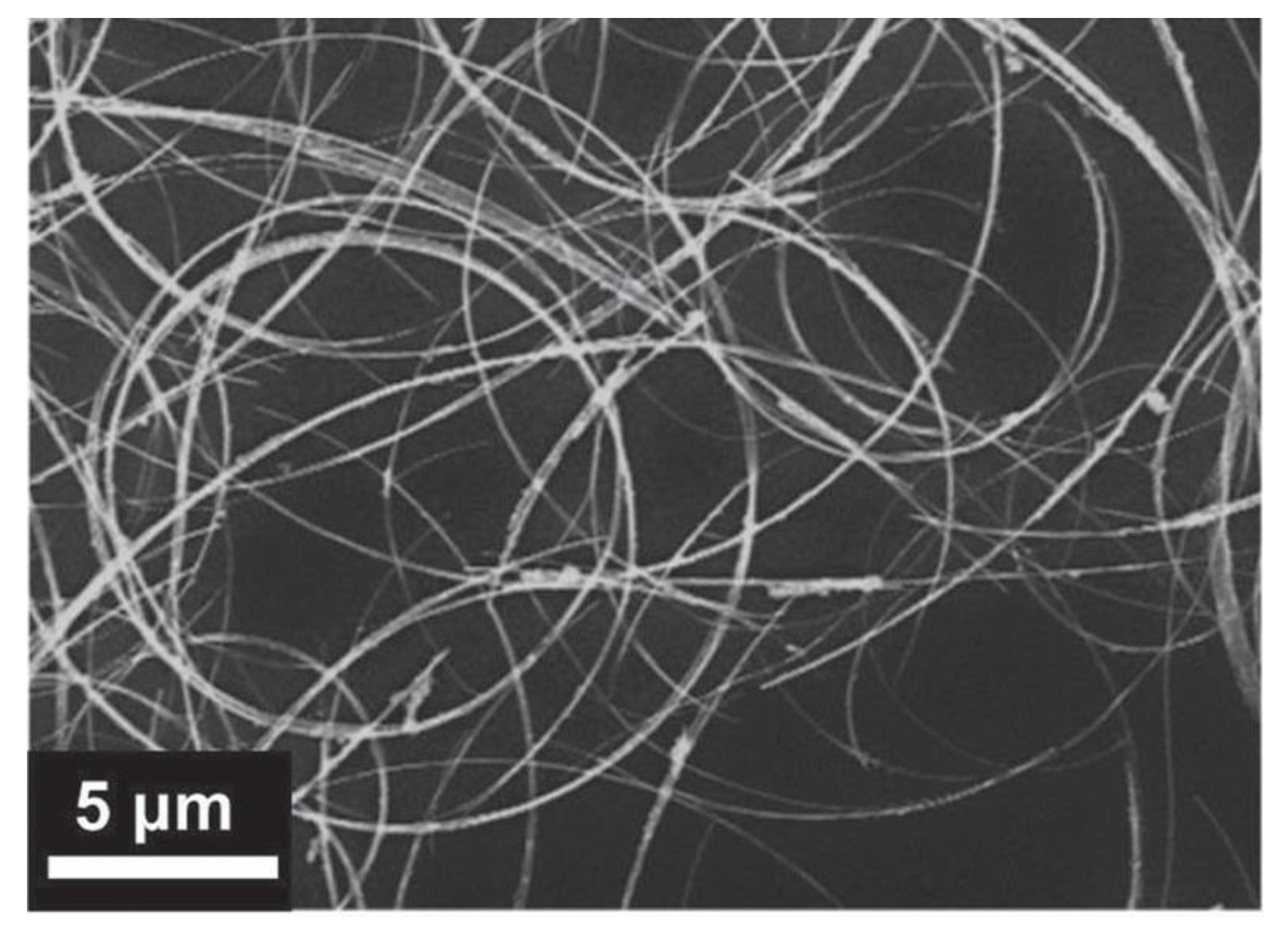
2. Electrical and Optical Properties of Cu NWs

When a thin film of nanomaterials is deposited onto a surface, such nanostructures form an interconnected network. When such nanostructures are electrically conductive, like in the case of metal NWs, electrical conduction can be measured only if there are conduction paths between electrodes, i.e., if the network is above the percolation threshold. It can be shown that, for such types of networks, the optimal conductivity is achieved for the structures with the longest length [25,26]. This is because electrons do not just travel ballistically through a single NW, but have to hop from one to another through junctions between electrodes. Junction resistance is thus another fundamental parameter that determines the overall network conductivity, more than the intrinsic material conductivity [27]. At the same time, for maximum transparency, the structures must have the smallest possible diameter [25,26]. Thus, the highest possible aspect ratio, intended as a length/diameter ratio, has to be sought after for the maximum conductivity associated with maximum transparency. Indeed, the scope of many synthetic methods has been to produce ultralong NWs. Moreover, a range of methods have been developed to reduce the junction resistance by melting the structures at the junction itself.
The first report in which Cu NWs were used as transparent electrodes appeared in 2010 from Rathmell et al. [18]. Here, Cu NWs were prepared by a chemical method, reducing Cu(NO3)2 by hydrazine in aqueous medium containing also NaOH and ethylenediamine at 80 °C. The authors obtained NWs with 90 nm average diameter and 9 μm average length, as shown by scanning electron microscopy (SEM) images in Figure 1. While Rs was as low as 15 Ω/sq at T = 65%, no data were reported at higher T, due to the large diameter of the NWs [18]. Such results were later improved by changing the synthesis method, using a heated reaction environment (80 °C) only for a short time, adding then polyvinylpyrrolidone (PVP) and cooling down the mixture in an ice bath [19]. In this way, NWs grew longer and thinner, with 20 μm length and 52 nm diameter, yielding networks with T up to 90% corresponding to Rs = 186 Ω/sq.
Other synthetic methods to improve NW morphology were also reported. Zhang et al. reported a synthesis in a liquid crystalline medium using hexadecylamine and cetyl trimethylammonium bromide (CTAB) and Cu acetylacetonate as precursor [28]. Such synthesis allowed the formation of NWs with 78 nm average diameter and length over 100 μm, with Rs = 90 Ω/sq at 90% transmittance. Compared to Ref. [19], for the same T the halving of Rs is most likely due to the much longer length, despite the wider diameter. Guo et al. obtained very thin NW (16 nm) with 40 μm length carrying out a reaction in oleylamine using a Ni-based catalyst [29]. A high transmittance of 93% was reported, associated with a low Rs of 51 Ω/sq. Compared to previous reports, the improvement here is mainly due to the very small NW diameter.
Another synthetic method to produce very long NWs was reported by Mayousse et al., who used octadecylamine and CuCl2 reacting at 165 °C for 140 h, to obtain films with Rs = 55 Ω/sq at T = 94% [30]. Unlike many other reports, the authors here also study haze, intended as the amount of light that is scattered rather than transmitted. While haze is detrimental for applications like displays or LED as they decrease transmittance, this can be seen as beneficial for solar cell applications as it allows the scattered light to be reabsorbed and thus utilized for energy production. Haze evaluation is thus related to the specific application. It was found that haze is somehow related to the transmittance, and is minimum for maximum transmittance [30]. Interestingly, the authors report diameters of a few hundred nm associated with lengths lower than 50 nm. The good performance is likely justified as the length distribution also includes structures as long as several hundred μm, which may be responsible for the low Rs at such high T. A similar finding was reported by Cui et al., who obtained NWs with 17 μm length and 17 nm diameter for a performance of 35 Ω/sq at T = 90% and haze down to 1% at T = 94% (Figure 2) [31]. The authors used a silane as reducing agent for CuCl2 in oleylamine and oleic acid. It has been shown that haze is related to NW diameter [32] so this is a further reason to try reducing NW diameter, where haze is to be minimized, beside improving T. Another method for improving T was found to be purification [33,34]. Here, NWs were purified by three cycles of centrifugation after adding n-hexane to the aqueous solution. NWs settled on the bottom of the hexane phase separating from other particles. T up to 97% were reported, associated to Rs = 103 Ω/sq. [33]. Alternatively, a method to obtain high purity NWs was proposed by Kim et al. by optimizing the relative concentrations of Cu precursor and capping agents [35].
A method for the production of NWs as long as 250 μm was reported by Zhang et al. by using polyhydric alcohols in presence of glucose and capping agents like oleylamine and oleic acid [36]. The number of hydroxyl groups in such alcohols was also found to influence the NW diameter, with more hydroxyls decreasing diameter. Here films with Rs = 92 Ω/sq at T = 91.5% were reported [36].
A synthetic process able to tune the diameters of Cu NWs was proposed by Wang et al., who could change the diameter from 20 to 90 nm by changing the concentration of halide ions [37]. They reported Rs ~60 Ω/sq at T = 90%.
The synthesis of curved Cu NWs was also reported. Yin et al. deposited these curved structures, like those shown in Figure 3, onto glass and polyimide (PI) claiming that the curved structure improves the network properties [38,39]. However, no significant improvement in Rs and T was reported compared to other reports. Zhang et al. also reported the synthesis of curved Cu NWs and their deposition on PET and PDMS, and showed T > 95% associated with Rs = 110 Ω/sq and haze < 2% [40].
In summary, this section provided an overview of the key electrical and optical properties related to transparent conductors, how they are affected by NW morphology and a brief account of the synthetic methods proposed to tune NW morphology in order to improve network performance.

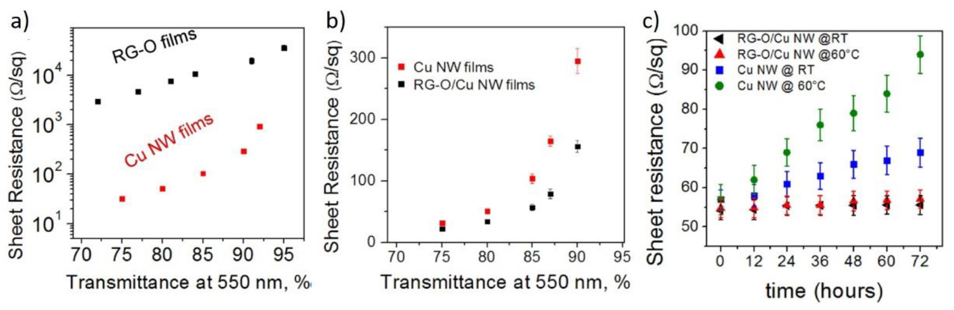
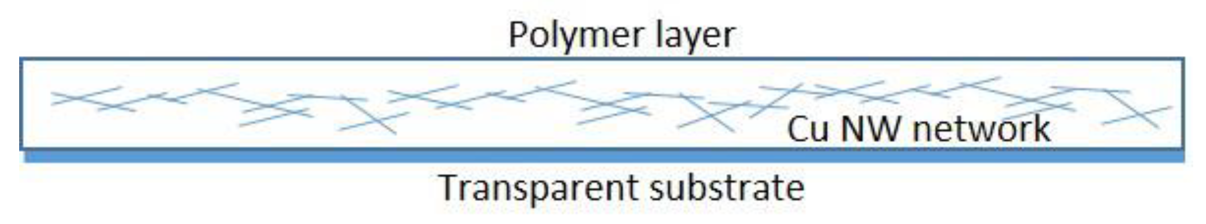
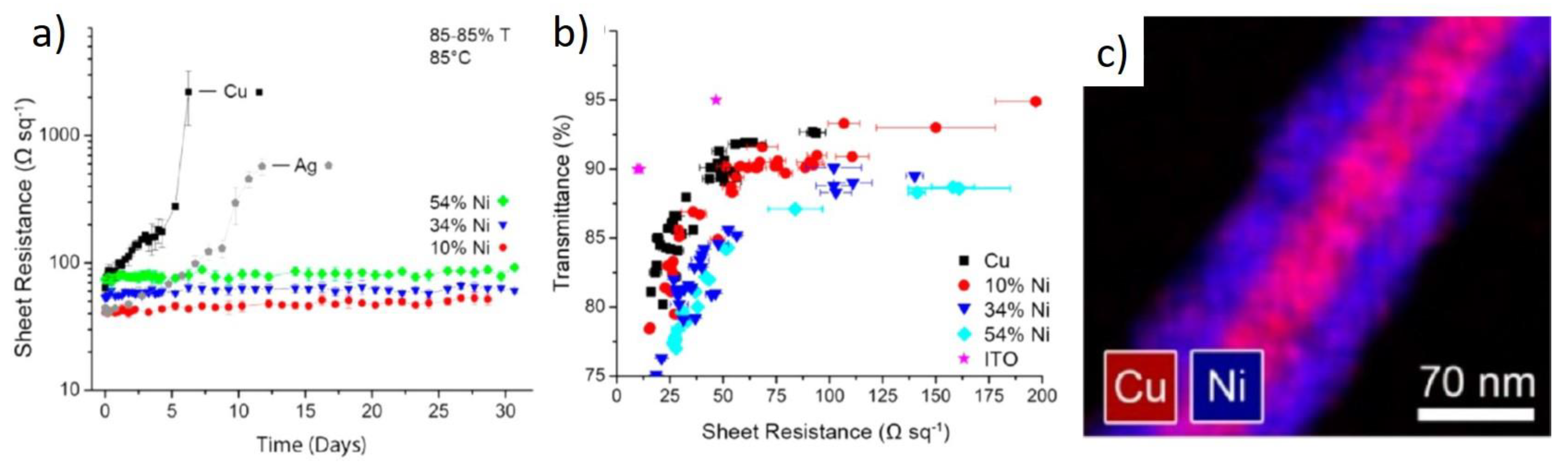
3. Oxidation Prevention

As already mentioned above, the major challenge facing Cu-based nanomaterials, including NWs, is oxidation, both as native oxide and as oxide forming over time in ambient conditions, both negatively affecting conductivity. While annealing in forming gas (5% H2 and 95% N2) is a typical way to remove the native oxide, other strategies are to be developed to protect from oxidation after synthesis [20]. For example, a UV treatment, followed by acid bath, was proposed to remove organic residues from the NW surface with subsequent performance improvement [41], though no information on the performance over time was given.
A popular method for oxidation protection is making core-shell structures with other materials, for example with Nickel [20,42,43]. This was first reported by Rathmell et al. who showed that for pristine Cu NW, when kept at 85 °C, Rs increased by two orders of magnitude within five days, while a layer of Ni kept Rs flat for at least up to 30 days (Figure 4a) [20]. The authors also reported that the presence of Ni significantly increased Rs. However, there is a clear advantage with the stability of the NWs (Figure 4b) [20]. Similar results were obtained by Stewart et al. who obtained Cu NW films deposited onto glass substrates dipped in acetic acid first to remove native oxide and then in an electroless plating Ni solution to form Cu-Ni core-shell NWs [42]. The same group later reported the synthesis of Cu-Ag core shell NWs using the same electroless plating Ag deposition [43]. The same acetic acid treatment could be repeated several times after reoxidation [34]. Unlike the case of Ni, Ag-coated Cu NWs did not show a decrease in optical and electrical performance. Xue et al. also reported Cu-Ni core-shell NWs, with findings similar to those reported above [44]. Niu et al. reported the epitaxial growth of 1–2 nm layers of Au onto Cu NWs, reporting a dramatic improvement of stability under high temperature (80 °C) and humidity (80%) [45].
Other than metals, oxides can also be viable protective coatings onto Cu NWs. For example, Chen et al. deposited metals like Zn, Sn and In by electrodeposition, followed by their oxidation, by hydrogen peroxide, into the corresponding transparent oxides [46]. A ZnO layer deposited by atomic layer deposition was used by Tigan et al. to improve the performance of transparent thin film heaters (see applications sections for more details) [47]. An Al-doped ZnO coating on the Cu NW was also proposed by Won et al. to convey ambient stability to the Cu NW network [48]. They also reported a lactic acid treatment to remove native oxide and other organic residues with no annealing.
The use of graphene and its related materials was also reported as a viable strategy to improve ambient stability of Cu NWs. Kholmanov et al. reported hybrid thin films of Cu NWs and reduced graphene oxide (RGO) [49]. They showed that while pure RGO thin films have Rs about two orders of magnitude higher than Cu NW films (Figure 5a), when combined together the Rs is decreased by about 2× from that of Cu NW films (Figure 5b). This is likely because the presence of RGO sheets lowers the junction resistance of Cu NWs and provides additional conduction paths. More importantly, Rs of such films is flat for at least 72 h at 60 °C (Figure 5c) [49]. Dou et al. reported Cu NWs wrapped with RGO with a slightly improved electrical properties and stability over 200 days [50]. Among the RGO-Cu NW films, those with lower T are the most stable, while those with higher T are more susceptible to oxidation with almost 2× Rs increase over 200 days. Core-shell Cu-graphene structures were obtained by Ahn et al. using a chemical vapor deposition process [51]. Here the NW network was tested for 30 days in ambient conditions with little Rs change, while for pure Cu NWs the Rs increased sharply after less than five days. Composites with graphene sheets which were exfoliated in the liquid phase were recently reported by Navik et al. [52]. Here the network stability was investigated for 46 days, showing a 27% increase in ambient condition and a 92% increase at 60 °C, with a significant improvement compared to bare Cu NW networks [52].
A different approach was recently proposed by Genlik et al., who applied a benzotriazole passivation layer [53]. Here benzotriazole, an organic corrosion inhibitor, made the Cu NWs stable under ambient conditions for 370 days without affecting the optoelectrical properties. Such higher stability was demonstrated also in more aggressive conditions like high temperatures p to 150 °C and humidity up to 90% [53].
In summary, this section provided an overview for the methods proposed in the literature for the protection of Cu NWs from oxidation under ambient or adverse conditions. Overall, all methods have in common a protective layer around the NW, which can be another metal, like Ni, metal oxides, another material like graphene, or molecules that act like corrosion inhibitors.

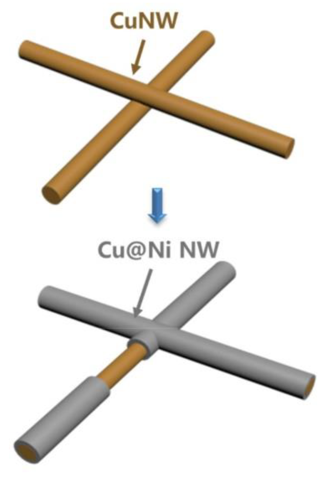
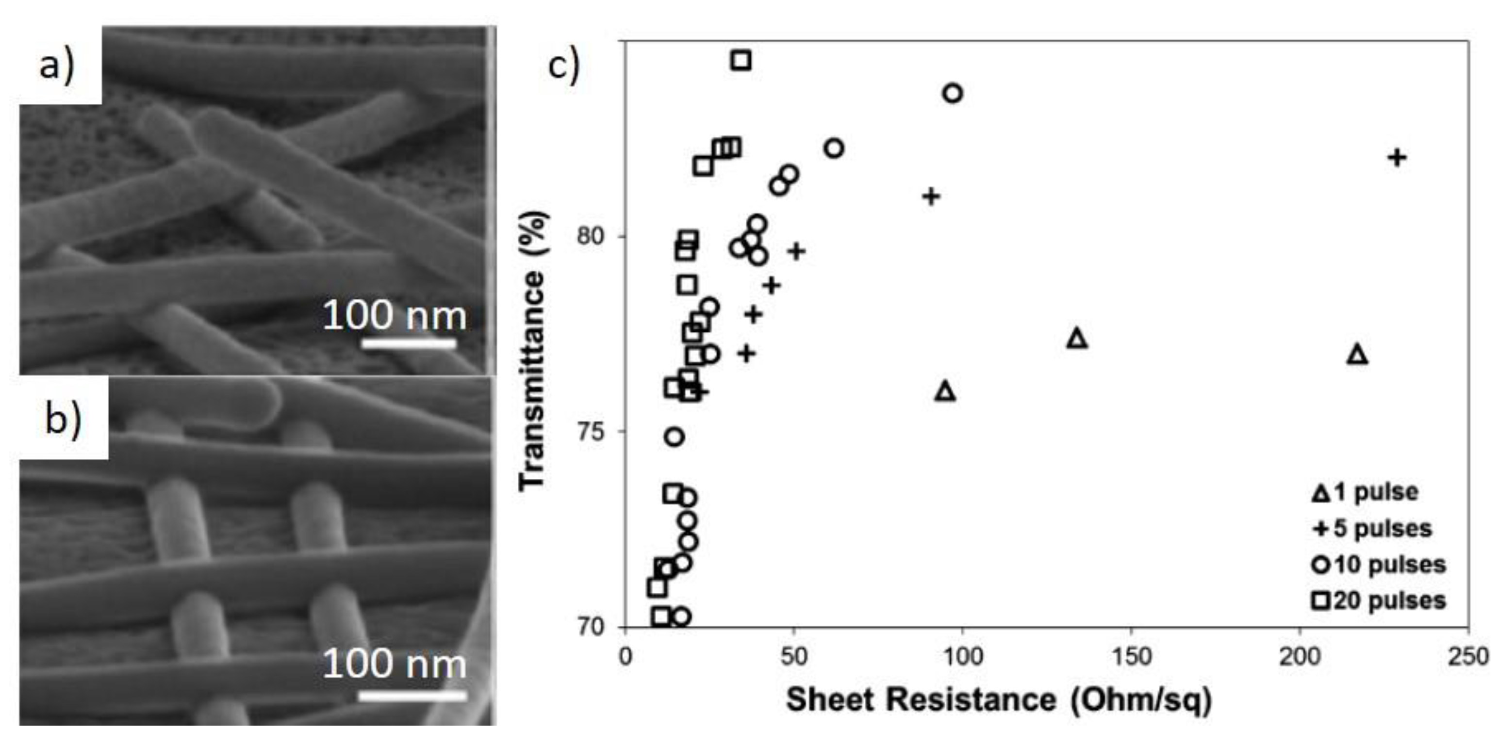
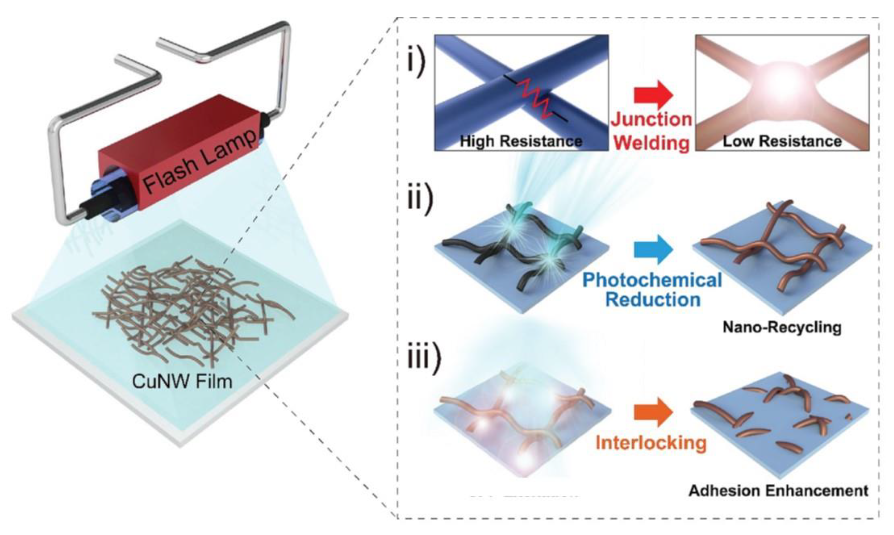
4. Joining of Nanowires

As already mentioned, junction resistance is a key factor that affects the conductivity of the whole network. Over the years, methods have then been developed to join, or weld, the NWs at the junctions, in order to eliminate, or cut down, the junction resistance. Most of these methods were firstly adopted for Ag NWs and involve the use of heat and/or light [54,55].
Such methods for Cu NWs also have the secondary effect of removing the oxide layer. Ding et al. proposed a high intensity pulsed light to induce both deoxygenation and welding [56]. Figure 6a,b shows tilted SEM images before and after the pulsed light treatment, and it can be observed that NWs are joint together after the treatment. Moreover, increasing the number of pulses dramatically improves the optical and electrical performance of the network (Figure 6c) [56], although no data were presented above 85% transmittance. Using the same method, the same group fabricated a polyurethane (PU) composite [57]. Here, the pulsed light also softened the PU matrix allowing embedding the NWs.
Wang et al. proposed a hydrogen plasma treatment to weld the NWs together, and at the same time improve their stability towards oxidation [58]. Here, the plasma treatment allowed cleaning the NW surface from organic residues from the synthesis process and oxide. At the same time, plasmonic effects allowed light intensity enhancement at the NW ends, causing thermal heating which induced melting [58]. Indeed, the Cu NWs had a plasmon resonance peak at 576 nm and a diameter of 60–100 nm, while the plasma had emission in the 570–610 nm range. Park et al. used flash light to both sinter Cu NWs, remove residues from the NW surface and induce adhesion to polyethyleneterephtalate (PET) by thermally melting the NW-PET interface (Figure 7) [59]. Similarly, plasmonic effects were exploited by Han et al. using a continuous 532 nm laser focused onto the NW network surface, for both preventing oxidation and welding the NWs [60]. Here, the Cu NWs had a diameter of 80–120 nm. Welding by electroplating was proposed by Zhao et al. who used the Cu NW film as electrode in a plating solution, then by applying voltage with a phosphor counter-electrode chemical welding was achieved [61].
A welding method not involving the use of any form of light was also proposed by Zhang et al., who synthesized core-shell NWs by electrodepositing Ni, Ag or Au-Ag on the Cu NW surface [62,63,64]. Here the metal shell, other than providing protection from oxidation, also provided welding by joining the NWs at the junctions, as shown in Figure 8.
In summary, methods for joining, or welding, Cu NWs mainly involve the use of light, which by thermal or plasmonic effects melt NWs at the junctions reducing the junction resistance. An electrodeposition method was also proposed, allowing welding as well as oxidation protection.

5. Mechanical Properties

One of the main drivers for the use of nanomaterials as transparent electrodes is their mechanical properties that, unlike ITO, guarantee flexibility upon bending and stretching. Cu NW are no exception to this, and many reports include mechanical testing, mainly bending tests performed over a large number of cycles. Table 1 summarizes the main results reported concerning mechanical testing of Cu NWs. It can be observed that in most cases the resistance of the NW network shows very little change under the length of the testing. In the case of stretching, it is interesting to note that the relative sheet resistance changes, R/R0, reported in Table 1, are obtained after the materials are subjected to a strain ranging from 50% to 250%.
Adhesion to a substrate is often a challenge for NW, which is rarely addressed in the literature. A simple tape test can be performed to address this matter, i.e., a sticky tape is pressed onto the substrate, bearing the NW network, and then peeled off. Yin et al. carried out this test for 10 times on their PU composite noting an Rs change <10% [39]. In this case, the tape had little consequences on the material as the NWs were mainly embedded within the PU matrix. Park et al. performed peeling tests on Cu NWs on PET substrates [59]. Here, while the adhesion was significantly improved after welding, after 5 cycles of peeling the Rs already increased by 10 times. Zhao et al. also performed a tape test on Cu NWs on PET, this time noting little resistance change (hardly quantifiable from the graph shown) after 10 peeling cycles on the network exposed to welding by electroplating [61].
In summary, this section provided a brief account of the mechanical properties of Cu NW-based network under a variety of testing like bending, stretching, twisting and adhesion.

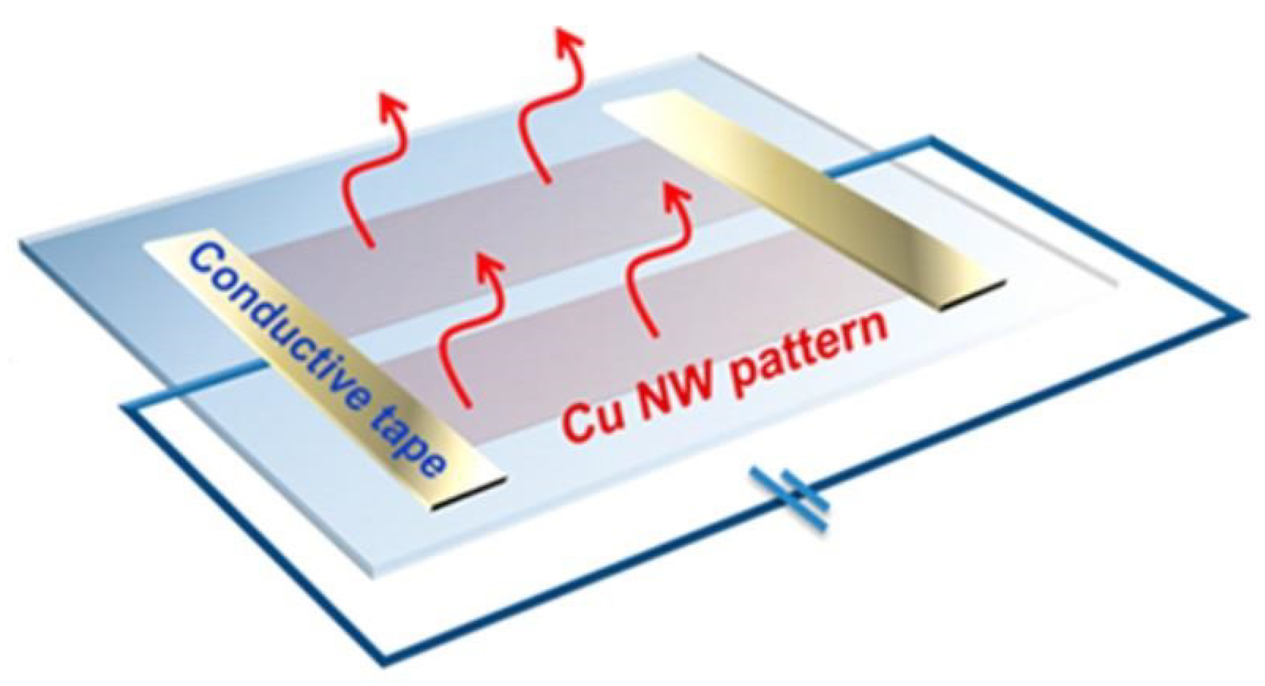
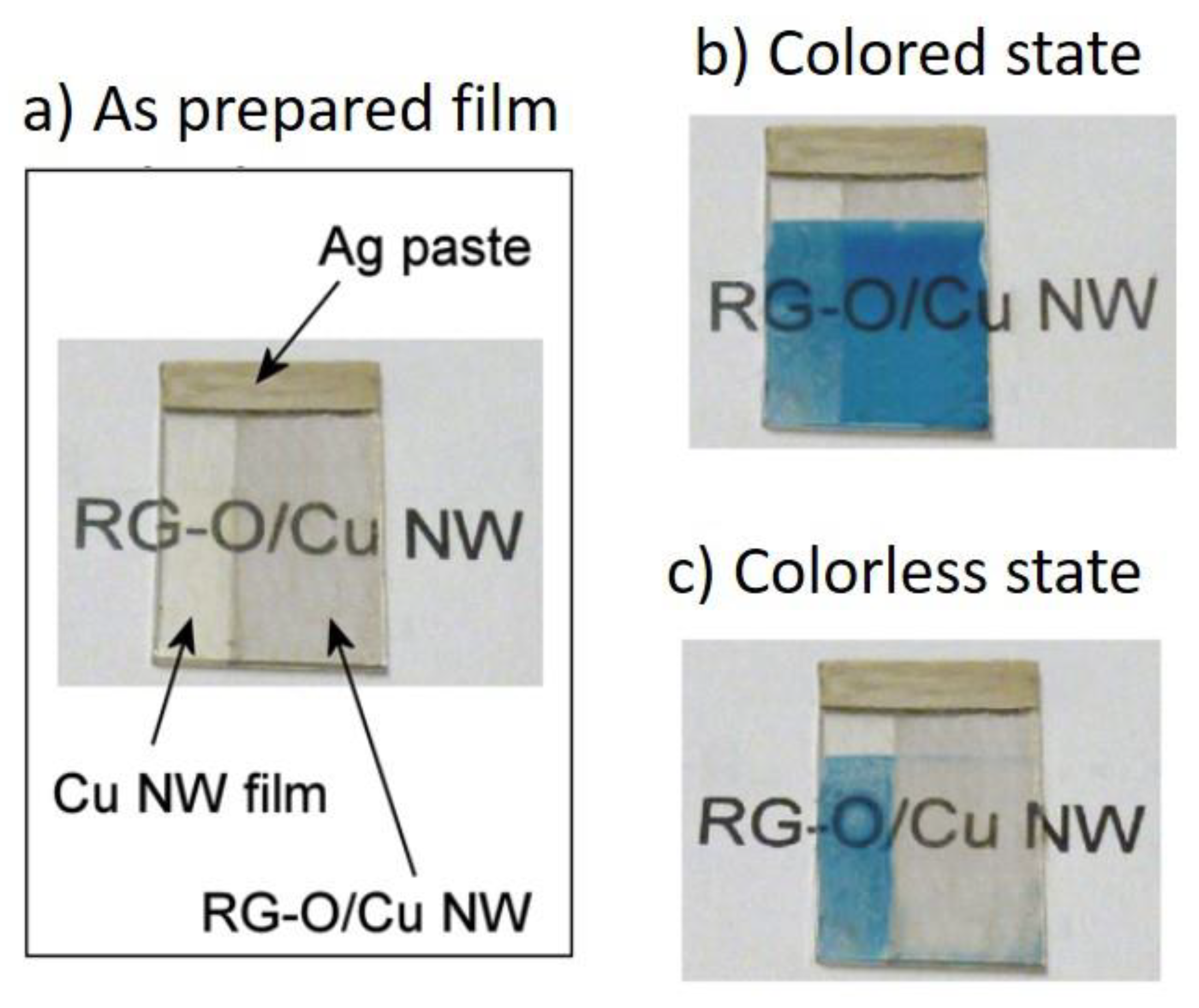
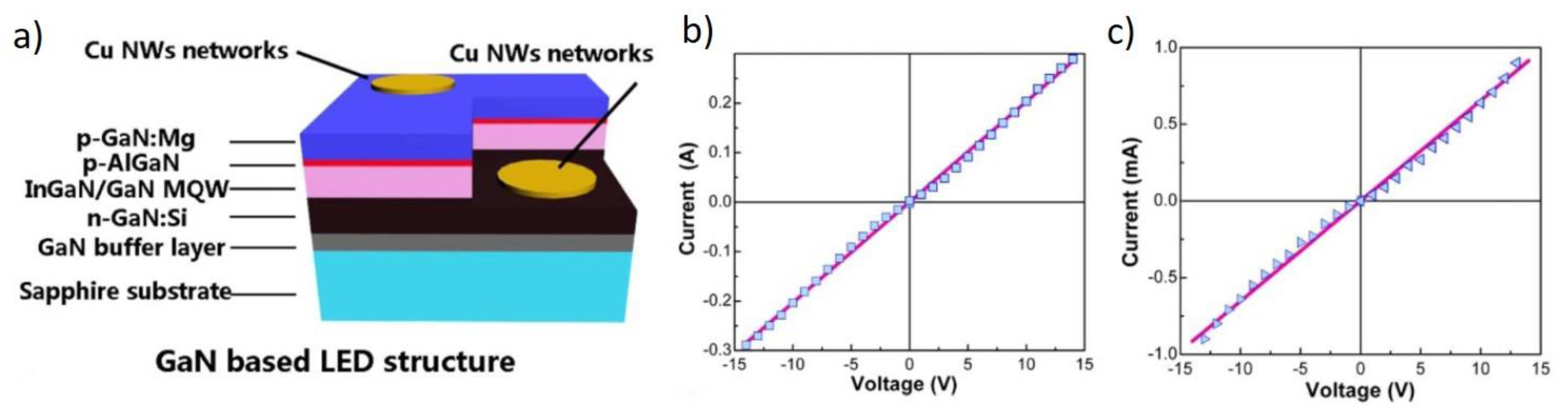
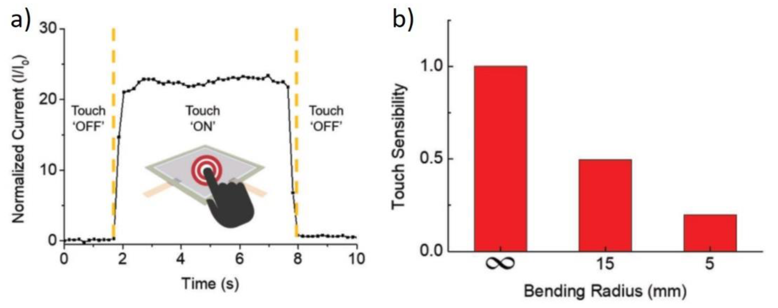
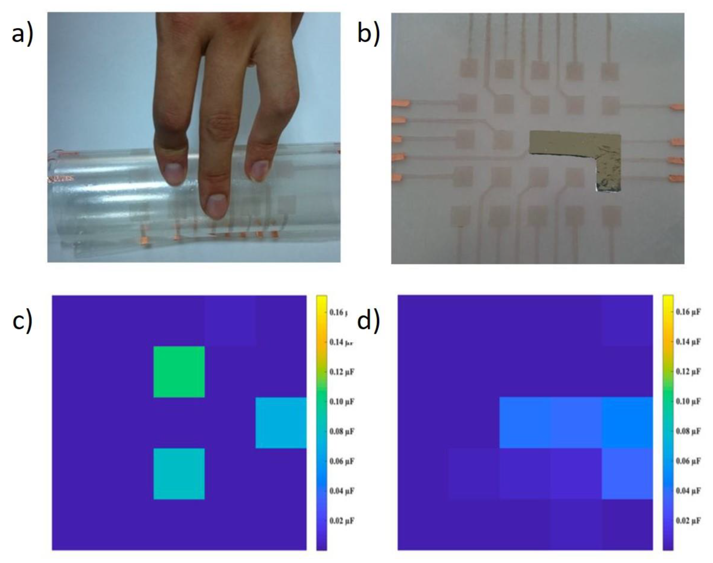
6. Applications of Copper Nanowires

Once demonstrated the viability of Cu NW based network as transparent conductors, a number of applications have also been demonstrated by several authors.
The first application was shown by Guo et al. who employed Cu NW transparent electrodes in a blue LED as ohmic contacts on n- and p-type GaN layers (Figure 9a) [29]. The ohmic contact is proved by the I-V curves in Figure 9b,c. The use in a GaN-based LED was also reported by Yoon et al. [69]. A LED structure was also demonstrated by Zhong et al. who fabricated a Cu NW based phosphorescent organic green LED with stable operation even under flexing [70]. In the same work, the authors proposed the application as transparent heater, working simply by Joule heating by applying a voltage to the ends of a Cu NW pattern, as shown in Figure 10 [70]. A transparent heater was also reported by Tigan et al. who used core-shell NWs with ZnO and Al2O3 [47]. Here, the authors employed this device for a defrosting application, reaching heating rate of 14 °C/s and maximum temperatures of 273 and 204 °C for Al2O3 and ZnO, respectively [47]. Flexible transparent heaters were similarly demonstrated with high heating uniformity and stable temperature output for up to 5 h by Zhang et al. [63,64]. Flexible transparent heaters were also demonstrated by Yu et al. using a transparent flexible conductive tape, obtained by transferring a Cu NW network from glass, where it was firstly deposited, onto a transparent tape [71]. The tape obtained had Rs ~20 Ω/sq at T = 80% and temperature up to 143 °C.
Another popular application that has been proposed for Cu NW networks is in solar cells. The first demonstration was reported by Sachse et al. who reported a small molecule organic solar cell with 3% efficiency [72]. Here, the authors used a poly(3,4-ethylenedioxythiophene) polystyrene sulfonate (PEDOT:PSS) layer for planarization applied on the NW network by spin-coating which, despite its hygroscopic and acidic properties, did not affect the stability of the Cu NWs. Stewart et al. reported an organic solar cell based on core-shell Ni-Cu NWs with 4.9% efficiency, again using a PEDOT-PSS layer on top of the NW network [42]. Similarly, Ohiienko et al. fabricated an organic solar cell with a very high efficiency of 7.31% [68]. Ahn et al. made a polymer solar cell with 4.04% efficiency using their Cu-graphene core-shell NWs and PEDOT:PSS as planarization layer [51]. This compared to a 1.90% efficiency for pure Cu NWs. Wang et al. reported an organic solar cell based on Cu NW network with 2.67% efficiency, where they used an in-situ polymerization method to make an acrylic polymer layer for planarization [58]. A simple scheme of the NW network-polymer assembly is shown in Figure 11. Table 2 summarizes the main information on the reported solar cell devices.
A very popular field of application is in the stretchable and wearable electronics, usually when the Cu NW are coupled with polymers like PU or PDMS. The first demonstration of a flexible touch sensor, based on capacitance change, was given by Mayousse et al. who fabricated a Cu NW composite with PEDOT:PSS [30]. Park et al. showed the operation of a touch-screen panel from Cu NWs on PET [59]. Here, while the device operated correctly, the counter-electrode was made of ITO, which may hinder the stability under bending. In the same work, the authors demonstrated a transparent resistive memory, again based on an ITO counter-electrode [59]. The device showed a good ON/OFF ratio of 103. Kim et al. proposed a flexible touch sensor based on their NW-PU composite [35]. Such device is able to produce a current when “touched”, i.e., a small pressure is applied (Figure 12a). This ability is maintained upon bending, although the response is significantly reduced (Figure 12b) [35]. Genlik et al. also demonstrated a transparent tactile sensor that mapped the pressure applied by finger touch or other objects (Figure 13) [53]. Zhang et al. demonstrated a wearable sensor using a NW-PDMS composite which is able to detect the movement of a finger joint with fast response [36].
Kholmanov et al. demonstrated the realization of an electrochromic device based on Prussian blue from their NW-RGO composites [49]. Such a device was fabricated depositing the dye between the NW-RGO based electrode and an ITO counter-electrode. The reduction of the Fe2+/Fe3+ mixture, typical of the Prussian blue dye, to Fe2+ upon applying a 0.6 V voltage reversibly changed the device color from blue to colorless, as shown in Figure 14 [49]. An electrochromic device was also recently demonstrated by Zhang et al. using polyaniline which was directly polymerized onto the Cu NW network [62]. Here, different colors were obtained by tuning the voltage. The device also worked for energy storage with a capacitance of 12 mF/cm2.
In summary, this section provided an overview of the applications proposed for Cu NW transparent electrodes. These include LEDs, solar cells, wearable electronics, energy storage and electrochromic devices.

7. Conclusions and Perspectives

This review covers the fundamental properties and the main challenges facing Cu NW based transparent electrodes. After briefly discussing the target properties that a NW network should have, in terms of Rs, T, NW length and diameter, Section 2 covers some of the reported synthetic strategies proposed to obtain long and/or thin NWs, which should be able to improve the network properties. In Section 3, a range of methods to prevent oxidation have been summarized. Such methods generally involve the production of core-shell systems, in which the shell is another metal, a transparent oxide or graphene. Section 4 summarizes the methods used to join, or weld, the NWs together, thus reducing the junction resistance and significantly decreasing Rs. Such methods generally involved the use of light, through lasers of flash lamps, also exploiting plasmonic effects. Section 5 covers the mechanical properties of Cu NW, summarizing the findings on the bending, stretching, folding and taping tests that have been reported in the literature. Finally, Section 6 summarizes the applications that have been proposed for Cu NW transparent conductors.
From what has been reported in this paper, it can be seen that some research and development areas for Cu NWs are more mature than others. For example, there is a vast number of papers already aiming to obtain the longest and/or the thinnest NWs. There is also enough evidence of the stability of this material under mechanical stress. However, adhesion to substrates is a challenge that has been so far poorly addressed and deserves new solutions, like for example surface treatments or encapsulation. The latter might also be a further solution for preventing oxidation, beside those presented in Section 3. As for applications, while promising, these have so far been developed as single components of more traditional systems. Scalability is also a challenge that has not yet been sufficiently addressed. If the adhesion and scalability will be satisfactorily addressed then, to the author’s opinion, Cu NWs may become competitive with other technologies.

Funding

This research received no external funding.

Institutional Review Board Statement

Not applicable.

Informed Consent Statement

Not applicable.

Data Availability Statement

Not applicable.

Conflicts of Interest

The authors declare no conflict of interest.

References

  1. Gordon, R.G. Criteria for Choosing Transparent Conductors. MRS Bull. 2000, 25, 52–57. [Google Scholar] [CrossRef] [Green Version]
  2. Chen, Z.; Cotterell, B.; Wang, W. The fracture of brittle thin films on compliant substrates in flexible displays. Eng. Fract. Mech. 2002, 69, 597–603. [Google Scholar] [CrossRef]
  3. Leterrier, Y.; Médico, L.; Demarco, F.; Månson, J.A.E.; Betz, U.; Escolà, M.F.; Kharrazi Olsson, M.; Atamny, F. Mechanical integrity of transparent conductive oxide films for flexible polymer-based displays. Thin Solid Film. 2004, 460, 156–166. [Google Scholar] [CrossRef]
  4. Rowell, M.W.; McGehee, M.D. Transparent electrode requirements for thin film solar cell modules. Energy Environ. Sci. 2011, 4, 131–134. [Google Scholar] [CrossRef]
  5. Barnes, T.M.; van de Lagemaat, J.; Levi, D.; Rumbles, G.; Coutts, T.J.; Weeks, C.L.; Britz, D.A.; Levitsky, I.; Peltola, J.; Glatkowski, P. Optical characterization of highly conductive single-wall carbon-nanotube transparent electrodes. Phys. Rev. B 2007, 75, 235410. [Google Scholar] [CrossRef]
  6. Geng, H.-Z.; Kim, K.K.; So, K.P.; Lee, Y.S.; Chang, Y.; Lee, Y.H. Effect of Acid Treatment on Carbon Nanotube-Based Flexible Transparent Conducting Films. J. Am. Chem. Soc. 2007, 129, 7758–7759. [Google Scholar] [CrossRef]
  7. Doherty, E.M.; De, S.; Lyons, P.E.; Shmeliov, A.; Nirmalraj, P.N.; Scardaci, V.; Joimel, J.; Blau, W.J.; Boland, J.J.; Coleman, J.N. The spatial uniformity and electromechanical stability of transparent, conductive films of single walled nanotubes. Carbon 2009, 47, 2466–2473. [Google Scholar] [CrossRef]
  8. Scardaci, V.; Coull, R.; Coleman, J.N. Very thin transparent, conductive carbon nanotube films on flexible substrates. Appl. Phys. Lett. 2010, 97, 023114. [Google Scholar] [CrossRef]
  9. Bae, S.; Kim, H.; Lee, Y.; Xu, X.; Park, J.-S.; Zheng, Y.; Balakrishnan, J.; Lei, T.; Ri Kim, H.; Song, Y.I.; et al. Roll-to-roll production of 30-inch graphene films for transparent electrodes. Nat. Nanotechnol. 2010, 5, 574–578. [Google Scholar] [CrossRef] [PubMed] [Green Version]
  10. De, S.; King, P.J.; Lotya, M.; O’Neill, A.; Doherty, E.M.; Hernandez, Y.; Duesberg, G.S.; Coleman, J.N. Flexible, Transparent, Conducting Films of Randomly Stacked Graphene from Surfactant-Stabilized, Oxide-Free Graphene Dispersions. Small 2010, 6, 458–464. [Google Scholar] [CrossRef]
  11. Becerril, H.A.; Mao, J.; Liu, Z.; Stoltenberg, R.M.; Bao, Z.; Chen, Y. Evaluation of Solution-Processed Reduced Graphene Oxide Films as Transparent Conductors. ACS Nano 2008, 2, 463–470. [Google Scholar] [CrossRef]
  12. Wang, X.; Zhi, L.; Müllen, K. Transparent, Conductive Graphene Electrodes for Dye-Sensitized Solar Cells. Nano Lett. 2008, 8, 323–327. [Google Scholar] [CrossRef] [PubMed]
  13. De, S.; Higgins, T.M.; Lyons, P.E.; Doherty, E.M.; Nirmalraj, P.N.; Blau, W.J.; Boland, J.J.; Coleman, J.N. Silver Nanowire Networks as Flexible, Transparent, Conducting Films: Extremely High DC to Optical Conductivity Ratios. ACS Nano 2009, 3, 1767–1774. [Google Scholar] [CrossRef] [PubMed]
  14. Hu, L.; Kim, H.S.; Lee, J.-Y.; Peumans, P.; Cui, Y. Scalable Coating and Properties of Transparent, Flexible, Silver Nanowire Electrodes. ACS Nano 2010, 4, 2955–2963. [Google Scholar] [CrossRef]
  15. Madaria, A.R.; Kumar, A.; Ishikawa, F.N.; Zhou, C. Uniform, highly conductive, and patterned transparent films of a percolating silver nanowire network on rigid and flexible substrates using a dry transfer technique. Nano Res. 2010, 3, 564–573. [Google Scholar] [CrossRef] [Green Version]
  16. Scardaci, V.; Coull, R.; Lyons, P.E.; Rickard, D.; Coleman, J.N. Spray Deposition of Highly Transparent, Low-Resistance Networks of Silver Nanowires over Large Areas. Small 2011, 7, 2621–2628. [Google Scholar] [CrossRef]
  17. USGS. Mineral Commodity Summaries 2021; USGS: Reston, VA, USA, 2021; p. 200.
  18. Rathmell, A.R.; Bergin, S.M.; Hua, Y.-L.; Li, Z.-Y.; Wiley, B.J. The Growth Mechanism of Copper Nanowires and Their Properties in Flexible, Transparent Conducting Films. Adv. Mater. 2010, 22, 3558–3563. [Google Scholar] [CrossRef]
  19. Rathmell, A.R.; Wiley, B.J. The Synthesis and Coating of Long, Thin Copper Nanowires to Make Flexible, Transparent Conducting Films on Plastic Substrates. Adv. Mater. 2011, 23, 4798–4803. [Google Scholar] [CrossRef]
  20. Rathmell, A.R.; Nguyen, M.; Chi, M.F.; Wiley, B.J. Synthesis of Oxidation-Resistant Cupronickel Nanowires for Transparent Conducting Nanowire Networks. Nano Lett. 2012, 12, 3193–3199. [Google Scholar] [CrossRef]
  21. Nam, V.B.; Lee, D. Copper Nanowires and Their Applications for Flexible, Transparent Conducting Films: A Review. Nanomaterials 2016, 6, 47. [Google Scholar] [CrossRef]
  22. Li, X.S.; Wang, Y.M.; Yin, C.R.; Yin, Z.X. Copper nanowires in recent electronic applications: Progress and perspectives. J. Mater. Chem. C 2020, 8, 849–872. [Google Scholar] [CrossRef]
  23. Zhao, S.; Han, F.; Li, J.; Meng, X.; Huang, W.; Cao, D.; Zhang, G.; Sun, R.; Wong, C.-P. Advancements in Copper Nanowires: Synthesis, Purification, Assemblies, Surface Modification, and Applications. Small 2018, 14, 1800047. [Google Scholar] [CrossRef] [PubMed]
  24. Wang, Y.M.; Yin, Z.X. Review of Wet Chemical Syntheses of Copper Nanowires and Their Recent Applications. Appl. Sci. Converg. Technol. 2019, 28, 186–193. [Google Scholar] [CrossRef]
  25. De, S.; King, P.J.; Lyons, P.E.; Khan, U.; Coleman, J.N. Size Effects and the Problem with Percolation in Nanostructured Transparent Conductors. ACS Nano 2010, 4, 7064–7072. [Google Scholar] [CrossRef]
  26. Forró, C.; Demkó, L.; Weydert, S.; Vörös, J.; Tybrandt, K. Predictive Model for the Electrical Transport within Nanowire Networks. ACS Nano 2018, 12, 11080–11087. [Google Scholar] [CrossRef]
  27. Nirmalraj, P.N.; Lyons, P.E.; De, S.; Coleman, J.N.; Boland, J.J. Electrical Connectivity in Single-Walled Carbon Nanotube Networks. Nano Lett. 2009, 9, 3890–3895. [Google Scholar] [CrossRef]
  28. Zhang, D.Q.; Wang, R.R.; Wen, M.C.; Weng, D.; Cui, X.; Sun, J.; Li, H.X.; Lu, Y.F. Synthesis of Ultralong Copper Nanowires for High-Performance Transparent Electrodes. J. Am. Chem. Soc. 2012, 134, 14283–14286. [Google Scholar] [CrossRef]
  29. Guo, H.; Lin, N.; Chen, Y.; Wang, Z.; Xie, Q.; Zheng, T.; Gao, N.; Li, S.; Kang, J.; Cai, D.; et al. Copper Nanowires as Fully Transparent Conductive Electrodes. Sci. Rep. 2013, 3, 2323. [Google Scholar] [CrossRef] [PubMed] [Green Version]
  30. Cui, F.; Yu, Y.; Dou, L.T.; Sun, J.W.; Yang, Q.; Schildknecht, C.; Schierle-Arndt, K.; Yang, P.D. Synthesis of Ultrathin Copper Nanowires Using Tris(trimethylsilyl)silane for High-Performance and Low-Haze Transparent Conductors. Nano Lett. 2015, 15, 7610–7615. [Google Scholar] [CrossRef]
  31. Mayousse, C.; Celle, C.; Carella, A.; Simonato, J.-P. Synthesis and purification of long copper nanowires. Application to high performance flexible transparent electrodes with and without PEDOT:PSS. Nano Res. 2014, 7, 315–324. [Google Scholar] [CrossRef]
  32. Khanarian, G.; Joo, J.; Liu, X.Q.; Eastman, P.; Werner, D.; O’Connell, K.; Trefonas, P. The optical and electrical properties of silver nanowire mesh films. J. Appl. Phys. 2013, 114, 024302. [Google Scholar] [CrossRef]
  33. Kang, C.X.; Yang, S.J.; Tan, M.; Wei, C.H.N.; Liu, Q.M.; Fang, J.; Liu, G. Purification of Copper Nanowires To Prepare Flexible Transparent Conductive Films with High Performance. Acs Appl. Nano Mater. 2018, 1, 3155–3163. [Google Scholar] [CrossRef]
  34. Hashimi, A.S.; Ginting, R.T.; Chin, S.X.; Lau, K.S.; Nazhif Mohd Nohan, M.A.; Zakaria, S.; Yap, C.C.; Chia, C.H. Fast microwave-assisted synthesis of copper nanowires as reusable high-performance transparent conductive electrode. Curr. Appl. Phys. 2020, 20, 205–211. [Google Scholar] [CrossRef]
  35. Kim, D.; Kwon, J.; Jung, J.; Kim, K.; Lee, H.; Yeo, J.; Hong, S.; Han, S.; Ko, S.H. A Transparent and Flexible Capacitive-Force Touch Pad from High-Aspect-Ratio Copper Nanowires with Enhanced Oxidation Resistance for Applications in Wearable Electronics. Small Methods 2018, 2, 1800077. [Google Scholar] [CrossRef]
  36. Zhang, Y.; Guo, J.; Xu, D.; Sun, Y.; Yan, F. Synthesis of Ultralong Copper Nanowires for High-Performance Flexible Transparent Conductive Electrodes: The Effects of Polyhydric Alcohols. Langmuir 2018, 34, 3884–3893. [Google Scholar] [CrossRef]
  37. Wang, X.; Wang, R.; Shi, L.; Sun, J. Kinetically controlled synthesis of Cu nanowires with tunable diameters and their applications in transparent electrodes. J. Mater. Chem. C 2018, 6, 1048–1056. [Google Scholar] [CrossRef]
  38. Yin, Z.; Song, S.K.; You, D.-J.; Ko, Y.; Cho, S.; Yoo, J.; Park, S.Y.; Piao, Y.; Chang, S.T.; Kim, Y.S. Novel Synthesis, Coating, and Networking of Curved Copper Nanowires for Flexible Transparent Conductive Electrodes. Small 2015, 11, 4576–4583. [Google Scholar] [CrossRef]
  39. Yin, Z.; Song, S.K.; Cho, S.; You, D.-J.; Yoo, J.; Chang, S.T.; Kim, Y.S. Curved copper nanowires-based robust flexible transparent electrodes via all-solution approach. Nano Res. 2017, 10, 3077–3091. [Google Scholar] [CrossRef]
  40. Zhang, Y.; Guo, J.N.; Xu, D.; Sun, Y.; Yan, F. Synthesis of ultrathin semicircle-shaped copper nanowires in ethanol solution for low haze flexible transparent conductors. Nano Res. 2018, 11, 3899–3910. [Google Scholar] [CrossRef]
  41. Lonne, Q.; Endrino, J.; Huang, Z.R. UV Treatment of Flexible Copper Nanowire Mesh Films for Transparent Conductor Applications. Nanoscale Res. Lett. 2017, 12, 577. [Google Scholar] [CrossRef] [Green Version]
  42. Stewart, I.E.; Rathmell, A.R.; Yan, L.; Ye, S.; Flowers, P.F.; You, W.; Wiley, B.J. Solution-processed copper–nickel nanowire anodes for organic solar cells. Nanoscale 2014, 6, 5980–5988. [Google Scholar] [CrossRef] [PubMed]
  43. Xue, J.; Song, J.; Zou, Y.; Huo, C.; Dong, Y.; Xu, L.; Li, J.; Zeng, H. Nickel concentration-dependent opto-electrical performances and stability of Cu@CuNi nanowire transparent conductors. RSC Adv. 2016, 6, 91394–91400. [Google Scholar] [CrossRef]
  44. Stewart, I.E.; Ye, S.; Chen, Z.; Flowers, P.F.; Wiley, B.J. Synthesis of Cu–Ag, Cu–Au, and Cu–Pt Core–Shell Nanowires and Their Use in Transparent Conducting Films. Chem. Mater. 2015, 27, 7788–7794. [Google Scholar] [CrossRef]
  45. Niu, Z.G.; Cui, F.; Yu, Y.; Becknell, N.; Sun, Y.C.; Khanarian, G.; Kim, D.; Dou, L.; Dehestani, A.; Schierle-Arndt, K.; et al. Ultrathin Epitaxial Cu@Au Core-Shell Nanowires for Stable Transparent Conductors. J. Am. Chem. Soc. 2017, 139, 7348–7354. [Google Scholar] [CrossRef] [Green Version]
  46. Chen, Z.F.; Ye, S.R.; Stewart, I.E.; Wiley, B.J. Copper Nanowire Networks with Transparent Oxide Shells That Prevent Oxidation without Reducing Transmittance. Acs Nano 2014, 8, 9673–9679. [Google Scholar] [CrossRef]
  47. Tigan, D.; Genlik, S.P.; Imer, B.; Unalan, H.E. Core/shell copper nanowire networks for transparent thin film heaters. Nanotechnology 2019, 30, 325202. [Google Scholar] [CrossRef]
  48. Won, Y.; Kim, A.; Lee, D.; Yang, W.; Woo, K.; Jeong, S.; Moon, J. Annealing-free fabrication of highly oxidation-resistive copper nanowire composite conductors for photovoltaics. NPG Asia Mater. 2014, 6, e105. [Google Scholar] [CrossRef] [Green Version]
  49. Kholmanov, I.N.; Domingues, S.H.; Chou, H.; Wang, X.; Tan, C.; Kim, J.-Y.; Li, H.; Piner, R.; Zarbin, A.J.G.; Ruoff, R.S. Reduced Graphene Oxide/Copper Nanowire Hybrid Films as High-Performance Transparent Electrodes. ACS Nano 2013, 7, 1811–1816. [Google Scholar] [CrossRef] [PubMed]
  50. Dou, L.T.; Cui, F.; Yu, Y.; Khanarian, G.; Eaton, S.W.; Yang, Q.; Resasco, J.; Schildknecht, C.; Schierle-Arndt, K.; Yang, P.D. Solution-Processed Copper/Reduced-Graphene-Oxide Core/Shell Nanowire Transparent Conductors. Acs Nano 2016, 10, 2600–2606. [Google Scholar] [CrossRef]
  51. Ahn, Y.; Jeong, Y.; Lee, D.; Lee, Y. Copper Nanowire–Graphene Core–Shell Nanostructure for Highly Stable Transparent Conducting Electrodes. ACS Nano 2015, 9, 3125–3133. [Google Scholar] [CrossRef]
  52. Navik, R.; Xiao, D.; Gai, Y.; Tan, H.; Zhao, Y. One-pot synthesis of copper nanowire-graphene composite with excellent stability and electrical performance for flexible electrodes. Appl. Surf. Sci. 2020, 527, 146694. [Google Scholar] [CrossRef]
  53. Polat Genlik, S.; Tigan, D.; Kocak, Y.; Ercan, K.E.; Cicek, M.O.; Tunca, S.; Koylan, S.; Coskun, S.; Ozensoy, E.; Unalan, H.E. All-Solution-Processed, Oxidation-Resistant Copper Nanowire Networks for Optoelectronic Applications with Year-Long Stability. ACS Appl. Mater. Interfaces 2020, 12, 45136–45144. [Google Scholar] [CrossRef]
  54. Garnett, E.C.; Cai, W.; Cha, J.J.; Mahmood, F.; Connor, S.T.; Greyson Christoforo, M.; Cui, Y.; McGehee, M.D.; Brongersma, M.L. Self-limited plasmonic welding of silver nanowire junctions. Nat. Mater. 2012, 11, 241–249. [Google Scholar] [CrossRef]
  55. Hu, A.; Peng, P.; Alarifi, H.; Zhang, X.Y.; Guo, J.Y.; Zhou, Y.; Duley, W.W. Femtosecond laser welded nanostructures and plasmonic devices. J. Laser Appl. 2012, 24, 042001. [Google Scholar] [CrossRef] [Green Version]
  56. Ding, S.; Jiu, J.; Tian, Y.; Sugahara, T.; Nagao, S.; Suganuma, K. Fast fabrication of copper nanowire transparent electrodes by a high intensity pulsed light sintering technique in air. Phys. Chem. Chem. Phys. 2015, 17, 31110–31116. [Google Scholar] [CrossRef] [PubMed]
  57. Ding, S.; Jiu, J.; Gao, Y.; Tian, Y.; Araki, T.; Sugahara, T.; Nagao, S.; Nogi, M.; Koga, H.; Suganuma, K.; et al. One-Step Fabrication of Stretchable Copper Nanowire Conductors by a Fast Photonic Sintering Technique and Its Application in Wearable Devices. ACS Appl. Mater. Interfaces 2016, 8, 6190–6199. [Google Scholar] [CrossRef]
  58. Wang, R.R.; Zhai, H.T.; Wang, T.; Wang, X.; Cheng, Y.; Shi, L.J.; Sun, J. Plasma-induced nanowelding of a copper nanowire network and its application in transparent electrodes and stretchable conductors. Nano Res. 2016, 9, 2138–2148. [Google Scholar] [CrossRef]
  59. Park, J.H.; Han, S.; Kim, D.; You, B.K.; Joe, D.J.; Hong, S.; Seo, J.; Kwon, J.; Jeong, C.K.; Park, H.-J.; et al. Plasmonic-Tuned Flash Cu Nanowelding with Ultrafast Photochemical-Reducing and Interlocking on Flexible Plastics. Adv. Funct. Mater. 2017, 27, 1701138. [Google Scholar] [CrossRef]
  60. Han, S.; Hong, S.; Ham, J.; Yeo, J.; Lee, J.; Kang, B.; Lee, P.; Kwon, J.; Lee, S.S.; Yang, M.Y.; et al. Fast Plasmonic Laser Nanowelding for a Cu-Nanowire Percolation Network for Flexible Transparent Conductors and Stretchable Electronics. Adv. Mater. 2014, 26, 5808–5814. [Google Scholar] [CrossRef]
  61. Zhao, L.; Yu, S.H.; Li, X.P.; Wu, M.Y.; Li, L.X. High-performance flexible transparent conductive films based on copper nanowires with electroplating welded junctions. Sol. Energy Mater. Sol. Cells 2019, 201, 110067. [Google Scholar] [CrossRef]
  62. Zhang, H.; Tian, Y.; Wang, S.; Huang, Y.; Wen, J.; Hang, C.; Zheng, Z.; Wang, C. Highly stable flexible transparent electrode via rapid electrodeposition coating of Ag-Au alloy on copper nanowires for bifunctional electrochromic and supercapacitor device. Chem. Eng. J. 2020, 399, 125075. [Google Scholar] [CrossRef]
  63. Zhang, H.; Wang, S.; Tian, Y.; Liu, Y.; Wen, J.; Huang, Y.; Hang, C.; Zheng, Z.; Wang, C. Electrodeposition fabrication of Cu@Ni core shell nanowire network for highly stable transparent conductive films. Chem. Eng. J. 2020, 390, 124495. [Google Scholar] [CrossRef]
  64. Zhang, H.; Wang, S.; Hang, C.; Tian, Y. Joining of copper nanowires by electrodepositing silver layer for high-performance transparent electrode. Weld. World 2021, 65, 1021–1030. [Google Scholar] [CrossRef]
  65. Hu, W.; Wang, R.; Lu, Y.; Pei, Q. An elastomeric transparent composite electrode based on copper nanowires and polyurethane. J. Mater. Chem. C 2014, 2, 1298–1305. [Google Scholar] [CrossRef]
  66. Aliprandi, A.; Moreira, T.; Anichini, C.; Stoeckel, M.A.; Eredia, M.; Sassi, U.; Bruna, M.; Pinheiro, C.; Laia, C.A.T.; Bonacchi, S.; et al. Hybrid Copper-Nanowire-Reduced-Graphene-Oxide Coatings: A “Green Solution” Toward Highly Transparent, Highly Conductive, and Flexible Electrodes for (Opto)Electronics. Adv. Mater. 2017, 29, 1703225. [Google Scholar] [CrossRef] [Green Version]
  67. Zhang, X.Y.; Tang, Z.; Tian, D.; Liu, K.Y.; Wu, W. A self-healing flexible transparent conductor made of copper nanowires and polyurethane. Mater. Res. Bull. 2017, 90, 175–181. [Google Scholar] [CrossRef]
  68. Ohiienko, O.; Oh, Y.-J. Preparation of narrow copper nanowires with less oxidized surface for flexible and transparent electrodes under octadecylamine. Mater. Chem. Phys. 2020, 246, 122783. [Google Scholar] [CrossRef]
  69. Yoon, H.; Shin, D.S.; Babu, B.; Kim, T.G.; Song, K.M.; Park, J. Control of copper nanowire network properties and application to transparent conducting layer in LED. Mater. Des. 2017, 132, 66–71. [Google Scholar] [CrossRef]
  70. Zhong, Z.; Lee, H.; Kang, D.; Kwon, S.; Choi, Y.-M.; Kim, I.; Kim, K.-Y.; Lee, Y.; Woo, K.; Moon, J. Continuous Patterning of Copper Nanowire-Based Transparent Conducting Electrodes for Use in Flexible Electronic Applications. ACS Nano 2016, 10, 7847–7854. [Google Scholar] [CrossRef]
  71. Yu, S.; Liu, Z.; Zhao, L.; Gong, B. High-performance flexible transparent conductive tape based on copper nanowires. Opt. Mater. 2021, 119, 111301. [Google Scholar] [CrossRef]
  72. Sachse, C.; Weiß, N.; Gaponik, N.; Müller-Meskamp, L.; Eychmüller, A.; Leo, K. ITO-Free, Small-Molecule Organic Solar Cells on Spray-Coated Copper-Nanowire-Based Transparent Electrodes. Adv. Energy Mater. 2014, 4, 1300737. [Google Scholar] [CrossRef]
Figure 1. SEM images from chemically produced Cu NW. (a) an low magnification entangled network of Cu NWs; (b) a high magnification view of individual Cu NWs. Adapted with permission from Ref. [18]. Copyright © 2021 WILEY-VCH Verlag GmbH & Co. KGaA, Weinheim.
Applsci 11 08035 g001
Figure 2. Haze vs. transmittance plot. Reprinted with permission from Ref. [31]. Copyright 2015 American Chemical Society.
Applsci 11 08035 g002
Figure 3. SEM image of curved Cu NWs. Reprinted with permission from Ref. [38]. © 2021 WILEY-VCH Verlag GmbH & Co. KGaA, Weinheim.
Applsci 11 08035 g003
Figure 4. Performance of Cu-Ni core shell NWs. (a) Rs over time of pure Cu NW compared with core-shell NWs with different fractions of Ni; (b) T vs. Rs plot of Cu NW and core-shell NWs; (c) energy dispersive X-Ray spectroscopy image of a Cu-Ni core-shell NW. Adapted with permission from Ref. [20]. Copyright 2012 American Chemical Society.
Applsci 11 08035 g004
Figure 5. (a) Rs vs. T comparison for pristing Cu NW and RGO films; (b) Rs vs. T comparisonof pristine Cu Nw films and NW-RGO composite films; (c) Rs evolution over time for pristine Cu NW and NW-RGO films at room temperature and at 60 °C. Adapted with permission from Ref. [49]. Copyright 2013 American Chemical Society.
Applsci 11 08035 g005
Figure 6. Tilted SEM images of Cu NW before (a) and after (b) welding by high intensity pulsed light; (c) T vs. Rs plot of Cu NWs exposed to increasing nmber of light pulses. Adapted with permission from Ref. [56]. Copyright 2015 Royal Society of Chemistry.
Applsci 11 08035 g006
Figure 7. Schematics of the flash lamp treatment process, allowing junction welding (i), photochemical reduction (ii) and interlocking (iii). Adapted with permission from Ref. [59]. © 2021 WILEY-VCH Verlag GmbH & Co. KGaA, Weinheim.
Applsci 11 08035 g007
Figure 8. Welding NWs by Ni electrodeposition. Reprinted with permission from Ref. [63]. Copyright (2020) Elsevier.
Applsci 11 08035 g008
Figure 9. (a) Scheme of the blue light LED stack; (b) I-V curve of n-GaN contact; (c) I-V curve of the p-GaN contact. Adapted with permission from Ref. [29].
Applsci 11 08035 g009
Figure 10. Scheme of a simple transparent heater. Reprinted with permission from Ref. [70]. Copyright 2016 American Chemical Society.
Applsci 11 08035 g010
Figure 11. Scheme of a NW network-polymer assembly.
Applsci 11 08035 g011
Figure 12. (a) Electrical response of a NW-PU touch sensor; (b) touch response under bending. Adapted with permission from Ref. [35]. Copyright © 2021 WILEY-VCH Verlag GmbH & Co. KGaA, Weinheim.
Applsci 11 08035 g012
Figure 13. Transparent flexible tactile sensor. (a) touch by fingers; (b) touch by an object; (c) sensor response to touch by fingers; (d) sensor response to touch by an object. Adapted with permission from Ref. [53]. Copyright 2020 American Chemical Society.
Applsci 11 08035 g013
Figure 14. Operation of an electrochromic device based on Cu NW-RGO composite. (a) As prepared film; (b) colored state; (c) beached state. Adapted with permission from Ref. [49]. Copyright 2013 American Chemical Society.
Applsci 11 08035 g014
Table 1. Summary of mechanical tests reported for Cu NWs. PDMS: polydimethylsiloxane.
Test TypeSubstrate/MatrixNumber of CyclesR/R0Ref.
BendingFiltration membrane10001[18]
BendingPET10001.33[19]
BendingPI100~1[29]
BendingPI20,000~1[60]
FoldingPI61.4[60]
StretchingEco-flex8501.1[60]
StretchingPU2001[65]
BendingPET12801.5[48]
BendingPET2000<1.1[38]
StretchingPU10002[57]
BendingPU1001.5[57]
BendingPET10,000<1.04[66]
BendingPU1000<1.1[39]
BendingPU500<1.1[67]
BendingPU1500<1.05[35]
BendingPET/PDMS1000~1.04[40]
StretchingPDMS10001.1[40]
TwistingPDMS10001.05[40]
BendingPET2000~1.2[62]
BendingPET2000<1.05[63]
BendingPET1000<1.05[64]
BendingPET10001.15[52]
BendingPET5001.33[68]
Table 2. Summary of solar cell devices made using Cu NWs as transparent electrode.
Solar Cell TypePlanarizationEfficiencyRef
OrganicPEDOT:PSS3%[72]
OrganicPEDOT:PSS4.9%[42]
OrganicPEDOT:PSS7.3%[68]
PolymerPEDOT:PSS4%[51]
OrganicAcrylic polymer2.7%[58]
Publisher’s Note: MDPI stays neutral with regard to jurisdictional claims in published maps and institutional affiliations.

