Abstract
We developed and tested a 2D periodic array of cold-electron bolometers arranged into a wideband frequency selective metasurface that absorbs more than 70% of the incident power in the frequency range 100–800 GHz. The array had 10 × 10 unit cells, each containing four bolometers incorporated into a ring. The chip with bolometers was mounted on the back side of the silicon lens without a back-reflector. Preliminary experiments demonstrated voltage responsivity as high as 109 V/W for the current-biased series array. Simulation of the noise performance shows realization of background noise-limited performance with NEPtot < NEPphot for the optical power load P0 > 15 pW. Results of numerical simulation made for the unit cell of the array are presented together with the equivalent diagram based on lumped network elements. The unit cell also was developed numerically to operate in two radiation modes.
1. Introduction
A cold-electron bolometer (CEB) is a cryogenic device with a tiny absorbing normal metal stripe connected to the two superconducting electrodes via superconductor–insulator–normal metal (SIN) tunnel junctions [1,2]. The incoming RF-signal increases the temperature of electrons in the normal metal, however in the presence of DC current hot electrons leave the absorber via SIN-junctions. An effect of electron cooling by the bias current increases the dynamic range of CEBs and reduces their noise equivalent power (NEP) [3,4,5]. Currently, the NEP level of CEBs is shown to be close to the photon noise limit [6,7], which makes CEBs attractive for balloon-borne radio astronomical missions such as the Large Scale Polarization explorer (LSPE) [8] and OLIMPO [9]. When CEBs are arranged into a periodic 2D array acting as a frequency selective surface (FSS) the incident RF signal is evenly distributed between all the bolometers. The resulting saturation RF-power of the array pixel is higher than that of a single bolometer by the factor which approximately equals the number of bolometers in the pixel. For achieving optimal NEP with reasonably high responsivity, the low-frequency impedance of the array should be matched to the impedance of the readout amplifiers. This can be done by an appropriate combination of parallel and series DC-connections between elementary unit cells [10]. It was shown in [11,12,13] that bolometric arrays consisting of the half-wavelength unit cells and fabricated on thick substrates provided 5–10% bandwidth. A reasonable agreement was obtained [12,13] between the experimentally measured frequency response and the one numerically calculated for the unit cell. In this paper we present the concept of an ultra-wideband array of CEBs with the unit cell size of the order of λ/10 at the central frequency 350 GHz.
2. Numerical Model
The effective surface impedance ZFSS (Ohm per square) of the periodic array of CEBs should be matched to the electrodynamic environment. Unlike conventional frequency selective surfaces, which do not contain active elements, a layout of the unit cell of the bolometric array must contain DC-lines for biasing and readout. It turns out that the way how DC-biasing issue is resolved determines the polarization of the incoming signal the array is sensitive to. The equivalent diagram of the array sitting on the back of a silicon lens without a back-reflector can be represented (see Figure 1) by the two impedances, vacuum impedance (ZVAC) and silicon impedance (ZSI) connected in parallel to ZFSS. They are frequency independent and correspond to the characteristic impedances of the vacuum and the silicon half-spaces. If ZFSS = 90 Ω then Pabs, the fraction of the RF-power coupled from ZSI to ZFSS, will be about 80% [14].
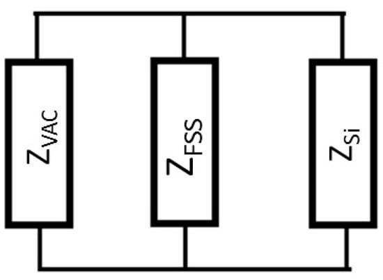
Figure 1.
Equivalent diagram.
Figure 2 shows the model of the unit cell with dimensions 64 μm × 64 μm in XY-plane and its SEM image. The array is designed for receiving linear Y-polarized signal corresponding to the Floquet mode #1 and coming from the silicon half-space. E-field of the mode#1 is parallel to the DC-biasing lines that provide ZFSS close to the optimal value 90 Ω in a wide frequency range. Gaps between the neighboring rings result in capacitive ZFSS and therefore poor matching with ZSI. The orthogonal mode #2 is sensitive to the gaps between the neighboring rings and has poor matching because of capacitive ZFSS. The unit cell has periodic boundaries in X and Y directions, while the two Floquet ports are defined at the boundaries corresponding to the maximum and the minimum of z-coordinates. These parts are touching vacuum and silicon spaces correspondingly. The reference planes of both ports are touching the array of model by a lumped element with a series connection of resistance R and capacitance C. For a real CEB, R is determined by the DC resistance of the normal absorber, while C is the capacitance of the two SIN-junctions connected in series to the absorber. The optimal capacitance C = 20 fF and the resistance R = 100 Ω for each CEB.

Figure 2.
Unit cell of the CEB array: (a) 3D model with lumped elements representing CEBs [14], (b) SEM-image.
Small unit cell size allows for absorption by the bolometric array in a wide range of both frequency and incidence angle φ. The dependence of Pabs as a function of frequency and φ computed for the two orthogonal modes is shown in Figure 3. In these simulations φ is defined in YZ-plane. The focus of a silicon lens is a waist of the Gaussian beam, where the condition of the planar normally incident wave is nearly satisfied. For normal incidence the array absorbs nearly 80% of mode#1 power in the range from 100 GHz to 800 GHz. However, Figure 3a demonstrates moderate Pabs for φ values up to 40 degrees. This fact makes the array promising for integration into a waveguide or a back-to-back horn, where the k-vector of the incident wave has tangential component to the plane of the absorbing array.
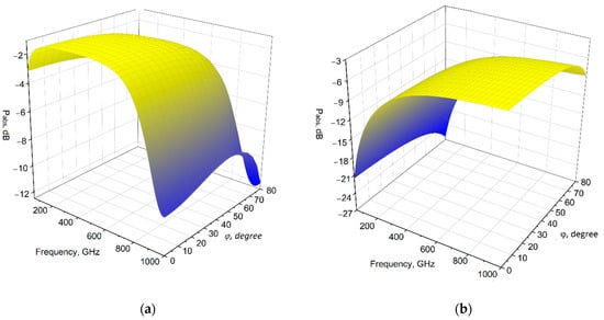
Figure 3.
Computed Pabs for the FSS unit cell: (a) mode #1, (b) mode #2.
With a new modification of the unit cell (see numerical model shown in Figure 4a) the array of CEBs absorbs an acceptable amount of power from two orthogonal modes. The equivalent network of a single ring with the four bolometers can be represented by that of a single bolometer and the inductance of the ring Lr excited by a plane wave (see Figure 4b). Capacitive coupling between the adjacent rings in the array is associated with capacitance Cr, which creates negative contribution to the imaginary part of ZFSS. Biasing wires between the rings can be represented by small resistance r connected in series with inductance Lw. Vertical wires seen by mode #1 have ohmic contacts to the rings, while horizontal wires seen by mode #2 with horizontal polarization have a thin SiO2 layer between the wire pad and the ring in the overlapping area that creates series capacitance Cw, such that Cw >> Cr. Impedance of wire inductance Lw is shunting large impedance of Cr and reduces its reactance to the value comparable to the reactance of the ring with the four CEBs. Both equivalent networks shown in Figure 4b and representing ZFSS are equivalent to a series resonant network, which impedance around the resonant frequency is real and equal to the resistance R = 100 Ω of the CEB.

Figure 4.
(a) Unit cell layout for dual mode sensing. (b) Equivalent circuits for ZFSS for two orthogonal modes of the Floquet port.
Figure 5 indicates calculated ZFSS for both modes. As is shown, both modes can see the DC-biasing wires (the horizontal and vertical wires) and capacitive coupling between two adjacent unit cells can be tuned out at around 350 GHz for mode#1 and 750 GHz for mode#2. Series capacitance Cw shifts the absorption frequency for mode#2 and increases the absorption bandwidth (see Figure 6). Figure 6a shows absorption of the waves coming from the silicon half-space for both orthogonal modes, Absorption of arbitrary polarization Pabs can be calculated as total absorption of different waves with amplitude a and random uniform distribution of polarization angle θ. The inset in Figure 6b shows vectors P1 and P2 corresponding to polarizations of mode #1 and mode #2. Pabs can be found by taking a simple integral:
where Pabs(1) is absorbed power of mode#1 and Pabs(2) is absorbed power of mode#2.
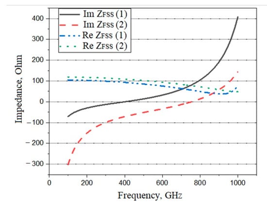
Figure 5.
Real and imaginary impedances of ZFSS calculated for mode#1 and mode#2.
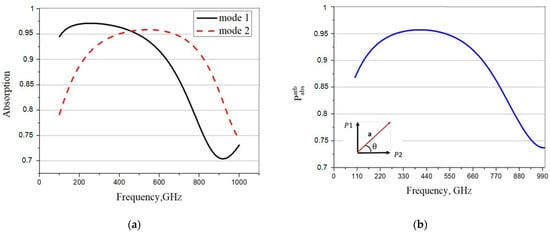
Figure 6.
(a) Pabs of mode#1 and mode#2, (b) Pabsarb of the unit cell for arbitrary polarization.
From Equation (1) the calculated absorbed power of both modes for the pattern of array with the optimized unit cell design as functions of frequency are provided and shown in Figure 6, which illustrates the results of a wideband of frequency range from 100 GHz to 1000 GHz. Figure 6a shows absorption for each mode separately and it can be seen for two modes the absorption is from 70% to more than 95%. According to Equation (1) the absorption power of the two modes can be concluded (see Figure 6b), which shows absorption more than 75% (from 75% to 95%).
3. Noise Analysis
In our noise analysis of the 2D CEB array we use the basic CEB model with a strong electrothermal feedback due to electron cooling [15,16] and the concept of series arrays in a current-biased mode [9]. The operation of a CEB array can be analyzed using the heat balance equation for a single CEB, taking into account the power distribution between the N × W bolometers:
Here, is the heat flow from the electron to the phonon subsystems in the absorber, Σ is a material constant, Λ is the volume of the absorber, Te and Tph are, respectively, the electron and phonon temperatures of the absorber, is the cooling power of the SIN tunnel junction, Rj is the sub-gap resistance of the tunnel junction, Ra is the resistance of the absorber, is the incoming RF power changes and P0 is absorbed signal power. We can separate Equation (2) into the time independent term,
and the time dependent term,
The first term in Equation (4), , is the cooling thermal conductance of the SIN junction that gives the negative electrothermal feedback (ETF); when this term is large, it reduces the temperature response, δΤ, because the cooling power, PSIN, compensates for the change of signal power in the bolometer. The second term in Equation (4), , is the electron-phonon thermal conductance of the absorber. From Equation (4), we can define an effective complex thermal conductance that controls the temperature response of the CEB to the incident signal power:
In analogy with TES [10], the effective thermal conductance of the CEB is increased by electron cooling (negative ETF). Here, we assume that the SIN tunnel junctions are current-biased, and the voltage is measured by a JFET amplifier. The responsivity, SV, is described by the voltage response to the incoming power:
In the second term of Equation (7),
is the cooling thermal conductance of the SIN junction, which provides some electron cooling and helps to avoid the overheating of the absorber.
Noise properties are characterised by the noise equivalent power (NEP), which is the sum of three contributions:
here, NEPe-ph is the noise associated with electron–phonon interaction:
In Equation (8), NEPSIN is the noise of the SIN tunnel junctions. The SIN noise has three components: the shot noise, 2eI/ S2I, the fluctuation of the heat flow through the tunnel junctions, and the correlation between these two processes:
Due to this correlation, the shot noise is increased by 30–50% in contrast to a CEB in voltage-biased mode, where strong anti-correlation decreases the shot noise.
The last term of Equation (8) depends on the voltage δV and the current δ I noise of a JFET, which are expressed in nV Hz−1/2 and pA Hz−1/2:
Estimations were made for the 150 GHz channel of balloon telescope LSPE.
The results of the simulation of the 2D array with JFET readout are shown in Figure 7.
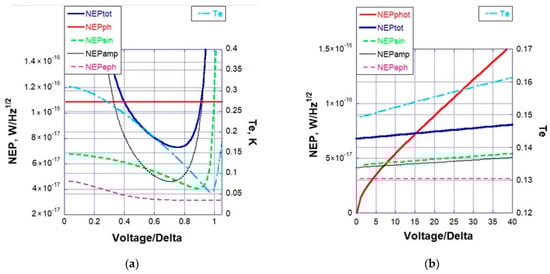
Figure 7.
(a) NEP components for the 2D periodic array of cold-electron bolometers with 10 × 10 unit cells, each containing four bolometers incorporated into a ring. Electron temperature, Te, is shown for both cases referring to the right axis. Parameters: f = 350 GHz, Po = 20 pW Iamp = 5 fA/Hz1/2, Vamp = 5 nV/Hz1/2 (JFET), R = 1 kΩ, Λ = 0.02 µm−3, T = 300 mK, (b) dependence of the noise component and electron temperature on optical power of absorbed signal.
Figure 7a shows realization of improved noise properties with total CEB noise NEPtot = 7 × 10⁻¹⁷ W/Hz1/2 less than photon noise of the signal NEPphot = 1.1 × 10⁻¹⁶ W/Hz1/2 for the array with a series and parallel combination of CEBs at the optical power load of 20 pW. Improvement of the NEP in 2D array is achieved due to distribution of the optical power load between 400 CEBs and the decrease in the amplifier noise, as determined by the product of the amplifier current noise and the Rd (11). Dynamic resistance of the array is matched to the noise impedance of the amplifier by proper combination of two CEBs in parallel (W = 2) and 64 CEBs in series (N = 64).
The total noise is determined mainly by the amplifier noise (JFET) (11) and the SIN tunnel junction noise (11). The electron–phonon noise (10) is small due to the small volume of the absorber and the low temperature. As we can see from Figure 7, the noise performance for the optical power load of 20 fW fits the requirements of NEPtot < NEPphot for R = 1 kΩ.
The results of the simulation for the 2D array for different optical power load, P0, are shown in Figure 7b. As we can see from Figure 7b, the noise performance for the optical power load P0 > 15 pW fits the requirements of background noise limited performance with NEPtot < NEPphot. Relatively large crossover power load is related with a large number of bolometers for wideband realization and consumption of large power load typical for the balloon experiments type of LSPE.
4. Experimental Check
As can be seen in Figure 8, the backward wave oscillator (BWO) acts as a tuneable wave source, whose signal is split by the chopper between the pyroelectric detector and the optical window of the He3 sorption cryostat. The pyroelectric is used as a reference detector for simultaneous calibration of power emission from BWO. Half of the BWO power passes through the chopper and enters the optical window of the cryostat. The window contains a combination of high- and low-pass quasioptical filters and a set of cold neutral density filters which act as cold attenuators to reduce the power of blackbody radiation from the room temperature background. After the filters, the signal is collected by a silicon lens mounted in a holder on the cryostat cold plate. The chip with an array of CEBs is placed on the back of the lens and DC-connected to the room temperature electronics via biasing filters containing cold resistors.
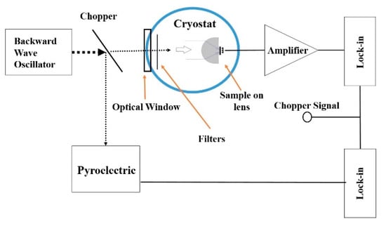
Figure 8.
A diagram of the experimental arrangement.
The resulting experimentally measured frequency response [14] normalized to the theoretically expected one is shown in Figure 9. The response decay above 350 GHz is associated with the cut-off frequency of the low-pass quasioptical filter at the cryostat optical window. Experiments with the blackbody radiations source demonstrated the voltage responsivity higher than 109 V/W [14].
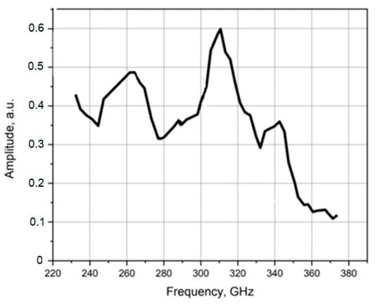
Figure 9.
Experimental frequency response of the CEB-array [14].
5. Conclusions
We developed and tested a new concept of the ultra-wideband array of CEBs consisting of sub-wavelength unit cells with voltage responsivity as high as 109 V/W and absorbing 80% of the incident power in the frequency range 100–800 GHz. Simulation of the noise performance shows realization of background noise limited performance with NEPtot < NEPphot for the optical power load P0 > 15 pW. We also optimized the structure for performance in two modes, so that we have a high level of the absorption powers for two modes.
Author Contributions
Conceptualization, L.S.K. and A.S.S.; methodology, L.S.K. and A.S.; numerical simulation, B.B.; formal analysis, L.S.K., B.B. and M.Y.L.; writing—original draft preparation, A.S.S., L.S.K. and B.B.; funding acquisition L.S.K. All authors have read and agreed to the published version of the manuscript. All authors have read and agreed to the published version of the manuscript.
Funding
This research was funded by Russian Science Foundation (Project No. 21-79-20227). The work of Alexander Sobolev was supported by the State Task.
Acknowledgments
The authors would like to greatly acknowledge M.A. Tarasov for stimulating discussions and for assistance in samples fabrication and experimental measurements.
Conflicts of Interest
The authors declare no conflict of interest.
References
- Kuzmin, L.S. Cold-Electron Bolometer. In BOLOMETERS; Intechweb.org ed.; Perera, A.G.U., Ed.; Intech: Rijeka, Croatia, 2012; p. 77. ISBN 978-953-510235-9. [Google Scholar]
- Tarasov, M.A.; Kuzmin, L.S.; Edel’man, V.S.; Mahashabde, S.; de Bernardis, P. Optical Response of a Cold-Electron Bolometer Array Integrated in a 345-GHz Cross-Slot Antenna. IEEE Trans. Appl. Supercond. 2011, 21, 3635–3639. [Google Scholar] [CrossRef]
- Kuzmin, L. Ultimate cold-electron bolometer with strong electrothermal feedback. Proc. SPIE 2004, 5498, 349–361. [Google Scholar]
- Kuzmin, L.; Agulo, I.; Fominsky, M.; Savin, A.; Tarasov, M. Optimization of electron cooling by SIN tunnel junctions. Supercond. Sci. Technol. 2004, 17, s400–s405. [Google Scholar] [CrossRef]
- Gordeeva, A.V. Record electron self-cooling in cold-electron bolometers with a hybrid superconductor-ferromagnetic nanoabsorber and traps. Sci. Rep. 2020, 10, 21961. [Google Scholar] [CrossRef] [PubMed]
- Gordeeva, A.V.; Zbrozhek, V.O.; Pankratov, A.L.; Revin, L.S.; Shamporov, V.A.; Gunbina, A.A.; Kuzmin, L.S. Observation of photon noise by cold-electron bolometers. Appl. Phys. Lett. 2017, 110, 162603. [Google Scholar] [CrossRef]
- Kuzmin, L.S.; Pankratov, A.L.; Gordeeva, A.V.; Zbrozhek, V.O.; Shamporov, V.A.; Revin, L.S.; Blagodatkin, A.V.; Masi, S.; de Bernardis, P. Photon-noise-limited cold-electron bolometer based on strong electron self-cooling for high performance cosmology missions. Commun. Phys. 2019, 2, 1–8. [Google Scholar] [CrossRef]
- Aiola, S.; Amico, G.; Battaglia, P.; Battistelli, E.; Baù, A.; De Bernardis, P.; Bersanelli, M.; Boscaleri, A.; Cavaliere, F.; Coppolecchia, A.; et al. The Large-Scale Polarization Explorer (LSPE). Proc. SPIE 2012, 8446, 84467A. [Google Scholar]
- Kuzmin, L. 2D Array of Cold-Electron Nanobolometers with Double Polarization Cross-Dipole Antennae. Nanoscale Res. Lett. 2012, 7, 224. [Google Scholar] [CrossRef] [PubMed]
- Masi, S.; Ade, P.; Boscaleri, A.; De Bernardis, P.; De Petris, M.; De Troia, G.; Fabrini, M.; Iacoangeli, A.; Lamagna, L.; Lange, A.; et al. OLIMPO: A Balloon-Borne, Arcminute-Resolution Survey of the Sky at mm and Sub-mm Wavelengths. In Proceedings of the 16th ESA Symposium on European Rocket and Balloon Programmes and related Research, ESA-SP 530, Sankt Gallen, Switzerland, 2–5 June 2003. [Google Scholar]
- Mahashabde, S.; Sobolev, A.; Tarasov, M.; Tsydanzhapov, G.; Kuzmin, L. Planar frequency selective bolometric array at 350 GHz. IEEE Trans. Terahertz Sci. Technol. 2015, 5, 37–43. [Google Scholar] [CrossRef]
- Mahashabde, S.; Sobolev, A.; Bengtsson, A.; Andren, D.; Tarasov, M.A.; Salatino, M.; De Bernardis, P.; Masi, S.; Kuzmin, L.S. A Frequency Selective Surface Based Focal Plane Receiver for the OLIMPO Balloon-Borne Telescope. IEEE Trans. Terahertz Sci. Technol. 2015, 5, 145–152. [Google Scholar] [CrossRef]
- Mahashabde, S.; Tarasov, M.A.; Salatino, M.; Sobolev, A.; Masi, S.; Kuzmin, L.S.; de Bernardis, P. A distributed-absorber cold-electron bolometer single pixel at 95 GHz. Appl. Phys. Let. 2015, 107, 092602. [Google Scholar] [CrossRef]
- Sobolev, A.S.; Beiranvand, B.; Chekushkin, A.M.; Kudryashov, A.V.; Tarasov, M.A.; Yusupov, R.A.; Gunbina, A.; Vdovin, V.F.; Edelman, V. Wideband metamaterial-based array of SINIS bolometers. EPJ Web Conf. 2018, 195, 05009. [Google Scholar] [CrossRef][Green Version]
- Kuzmin, L. Optimization of the Hot-Electron Bolometer for Space Astronomy. In The International Workshop on Superconducting Nano-Electronics Devices; Pekola, J., Ruggiero, B., Silvestrini, P., Eds.; Springer: Boston, UK, 2002; pp. 145–154. [Google Scholar]
- Golubev, D.; Kuzmin, L. Nonequilibrium theory of a hot-electron bolometer with normal metal-insulator-superconductor tunnel junction. J. Appl. Phys. 2001, 89, 6464–6472. [Google Scholar] [CrossRef]
Publisher’s Note: MDPI stays neutral with regard to jurisdictional claims in published maps and institutional affiliations. |
© 2021 by the authors. Licensee MDPI, Basel, Switzerland. This article is an open access article distributed under the terms and conditions of the Creative Commons Attribution (CC BY) license (https://creativecommons.org/licenses/by/4.0/).