Abstract
To improve the power of reference wavefront generated by reference wavefront source (RWS) based on silicon nitride (SiN) waveguide in point diffraction interferometer (PDI), we design the Y-branch coupler and grating coupler, and then compare the maximum coupling efficiency, 3 dB fabrication tolerance, 3 dB alignment tolerance and polarization dependent loss of two couplers. Our results show that grating coupler has higher coupling efficiency, lower etching difficulty and alignment difficulty, while Y-branch coupler has lower coating difficulty. To get the maximum efficiency, mode in the fiber must be TE mode no matter for grating coupler or Y-branch coupler. This paper improves the power of the wavefront by selecting appropriate fiber-to-waveguide couplers for waveguide RWS. PDI based on the power improved waveguide RWS is expected to be used in many measurement fields.
1. Introduction
Reference wavefront used in traditional interferometers [1] such as Twyman–Green interferometer and Fizeau interferometer is generated by reflection of a standard reference mirror, so accuracy of the reference wavefront is limited by fabrication accuracy of the standard reference mirror which is usually not better than (). Different from above interferometers, reference wavefront used in the point diffraction interferometer (PDI) [2,3,4,5,6,7] is generated by a diffraction element called reference wavefront source (RWS). RWS generates a nearly ideal spherical reference wavefront by diffraction at a small aperture of micrometer diameter, so accuracy of the reference wavefront is not limited by a standard reference mirror and can reach sub-nanometer scale. To improve the accuracy, numerical aperture (NA), and power of the reference wavefront, and further expand the application of PDIs, researchers have proposed and made various RWSs.
Pinhole RWS and fiber RWS are two commonly used RWSs. Pinhole RWS [8,9,10,11] is made by etching a submicron pinhole on the metal film. Such a small pinhole can generate a high accuracy spherical reference wavefront and its NA is up to 0.3, but low light transmittance of this small pinhole () seriously reduces the power of the reference wavefront [12]. Pinhole RWS can also be fabricated by other materials like liquid crystal [13] or metal wire grid [14], but these pinhole RWSs also have the above problems.
Fiber RWS [12,15,16,17] generates the reference wavefront by diffraction at the end face of the single-mode fiber (SMF). Due to high light transmittance of the SMF, power of the generated reference wavefront is high [12]. But due to limitation of the SMF core diameter (3–5 µm) [17], NA of this reference wavefront is usually less than 0.2, which greatly limits the NA of the optical element to be tested. Using a special SMF with a submicron end face is an effective way to improve the NA of the reference wavefront, but this kind of SMF is difficult to fabricate and clamp.
To make the reference wavefront have high accuracy, NA, and power simultaneously, our group has designed a new RWS based on the silicon nitride (SiN) waveguide. Due to high refractive index difference between the SiN core () and silicon dioxide (SiO2) cladding (), light in the waveguide is firmly confined in the core whose cross-section side length is 0.25 µm, and propagates along the core to the output facet. Then, light is diffracted at the output facet, and spherical reference wavefront is generated. NA of this reference wavefront is more than 0.5, and root-mean-square (RMS) value is less than 0.03 nm. Power of this reference wavefront is mainly determined by coupling efficiency between the SMF and waveguide RWS. To get the maximum coupling efficiency, two fiber-to-waveguide couplers called Y-branch coupler [18,19,20] and grating coupler [21,22,23] are designed by numerical simulation. Then, coupling efficiency, 3 dB alignment tolerance, 3 dB fabrication tolerance, and polarization-dependent loss of two couplers are compared.
Rest of this paper is organized as follows. In Section 2, structure of the waveguide RWS and its operation are first introduced. Then, accuracy, NA and power of the reference wavefront are analyzed. In Section 3 and Section 4, Y-branch coupler and grating coupler are introduced in detail, including structure of the coupler, key parameters affecting the coupling efficiency, fabrication difficulty, alignment difficulty, and polarization-dependent loss. Y-branch coupler and grating coupler are compared in Section 5. In Section 6, a summary of this paper is made.
In this paper, numerical simulation is performed based on the finite difference time domain (FDTD) method. In the simulation, wavelength is 532 nm, refractive index of SiN is 1.96, refractive index of SiO2 is 1.48, diameter of the SMF core is 3 µm, refractive index of the SMF core is 1.4620, and refractive index of the SMF cladding is 1.4571. TE mode refers to the mode whose main component is along the direction in the plane when electric field propagates along the direction, and TM mode refers to the mode whose main component is along the direction. For convenience, these will not be repeated in the rest of the paper.
2. Reference Wavefront Source Based on SiN Waveguide
In this section, structure of the waveguide reference wavefront source (RWS) and its principle to generate the reference wavefront are introduced firstly. Then, important parameters of the waveguide RWS that influence the accuracy, numerical aperture (NA), and power of the reference wavefront are mentioned.
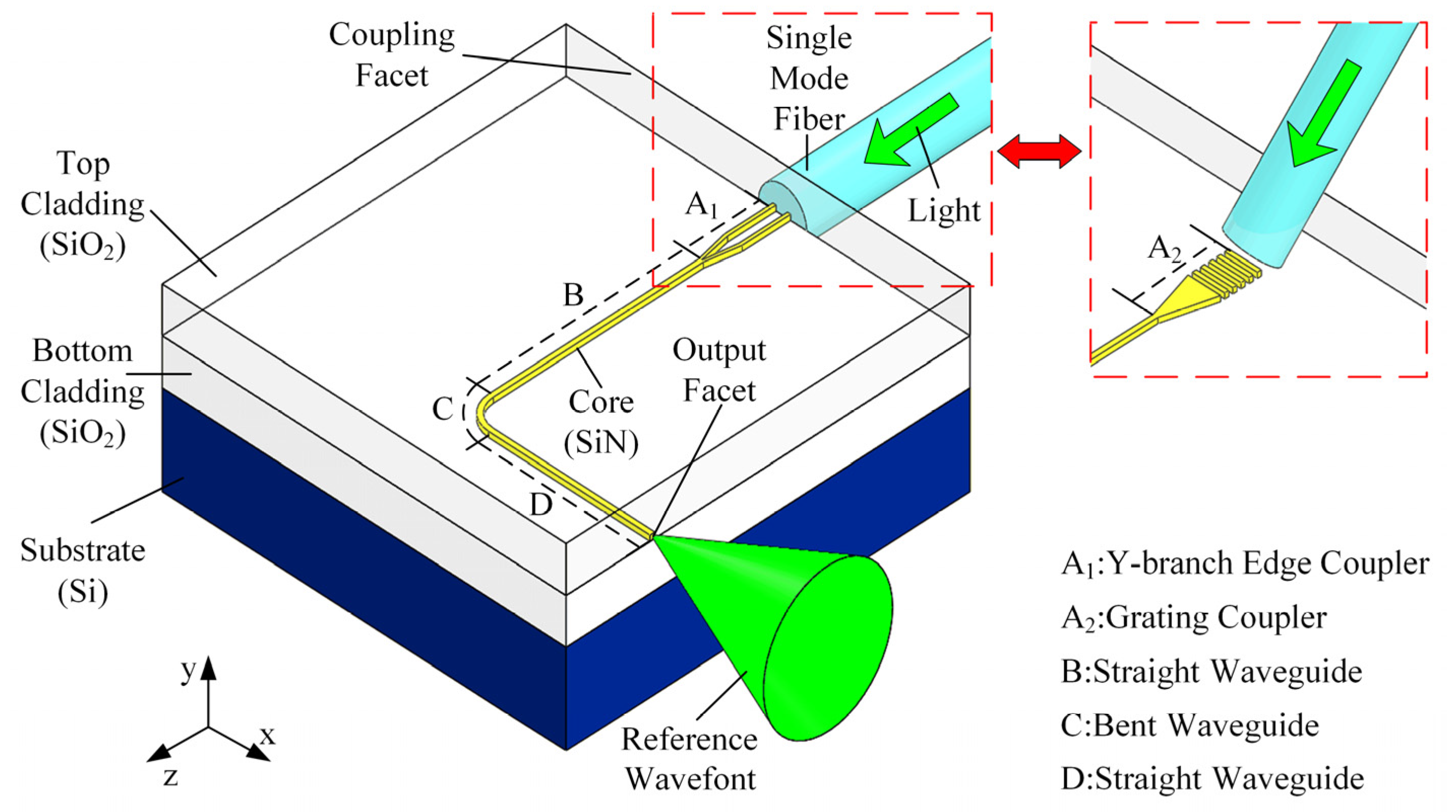
As shown in Figure 1, structure of the waveguide RWS is similar to the buried waveguide: silicon nitride (SiN) core with a thickness of 250 nm in the direction is buried between the silicon dioxide (SiO2) bottom cladding of 2.52 µm thickness and SiO2 top cladding of 2 µm thickness. SiO2 bottom cladding is located on the silicon (Si) substrate of 3 mm thickness. This waveguide RWS can be divided into four parts and each part has its function. Part A1 (Y-branch Coupler) or Part A2 (grating coupler) is used to improve the coupling efficiency between the single-mode fiber (SMF) and waveguide, and further increase the power of the reference wavefront. Therefore, fiber-to-waveguide coupler is the most important part in the design of the waveguide RWS. Part B and Part C are the straight waveguide. Part C is a bent waveguide with the sector angle of . This bent waveguide makes the reference wavefront perpendicular to the incident light, which avoids the interference between them.
Figure 1.
Structure of the waveguide reference wavefront source (RWS). Part A1 or A2 is a fiber-to-waveguide coupler. Part B and D are straight waveguides. Part C is a bent waveguide.
Waveguide RWS generates the spherical reference wavefront by diffraction at the output facet of the SiN core. This process is as follows: 532 nm incident light provided by the laser propagates to the fiber-to-waveguide coupler along the SMF. This incident light can be coupled into the waveguide either by the Y-branch coupler (Part A1) or the grating coupler (Part A2) and then propagates along the core. Due to high refractive index difference between the SiN core and SiO2 cladding, light in the waveguide is strongly confined in the sub-micron core during the propagation. Finally, light arrives at the output facet and spherical reference wavefront is generated by diffraction.
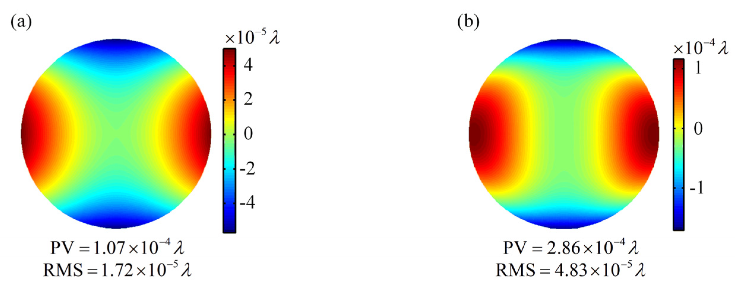
Accuracy and numerical aperture (NA) of the reference wavefront are determined by the size of the core cross-section ( cross-section of the core in Figure 1). SiN core of the waveguide RWS has a square cross-section of 0.25 µm in length, which satisfies the single-mode propagation condition. Accuracy and NA of the reference wavefront generated by this waveguide RWS are calculated by numerical simulation and results are shown in Figure 2. When NA of the reference wavefront is 0.3, peak-to-valley (PV) value and root-mean-square (RMS) value are and (), respectively. When NA increases to 0.5, PV value and RMS value are and , respectively. Even if NA of the reference wavefront reaches 0.5, RMS value is still less than 0.03 nm. Such a high accuracy reference wavefront cannot be generated by a pinhole RWS or fiber RWS.
Figure 2.
Accuracy of the reference wavefront generated by waveguide RWS when numerical aperture (NA) is (a) 0.3 or (b) 0.5.
Power of the reference wavefront is determined by the coupling efficiency between the SMF and waveguide. Therefore, an optimal fiber-to-waveguide coupler must be designed to improve the coupling efficiency. To provide a reliable reference for the selection of a fiber-to-waveguide coupler, Y-branch coupler and grating coupler are compared in detail, including their max coupling efficiency, 3 dB fabrication tolerance, 3 dB alignment tolerance and polarization-dependent loss.
3. Y-Branch Coupler
Using the Y-branch coupler is an effective way to improve the coupling efficiency between the single-mode fiber (SMF) and waveguide. In this section, firstly, structure of the Y-branch coupler is introduced and its key parameters are optimized to get the maximum coupling efficiency. Secondly, to quantitatively evaluate the fabrication difficulty and alignment difficulty of the coupler, 3 dB fabrication tolerance, 3 dB alignment tolerance, and polarization-dependent loss are analyzed, respectively.
3.1. Structure of the Y-Branch Coupler
Figure 3 shows the structure of the Y-branch coupler, including the input part and branch part. There are two identical and parallel straight structures in the input part. Width of each straight structure is and gap between two straight structures is . In the branch part, two straight structures merge into one and length of this part is . Height of the Y-branch coupler along the direction is 250 nm, which is consistent with the height of the silicon nitride (SiN) core.
Figure 3.
Structure of the Y-branch coupler. (a) Three-dimensional view; (b) Top view.
To get the maximum coupling efficiency, the SMF should be aligned to the Y-branch coupler center and the two should be as close as possible. Coupling efficiency of the Y-branch coupler can be calculated as follow:
where denotes the matching degree between the mode in the SMF and mode in the input part, denotes the transmission efficiency of the branch part.
3.2. Parameter Optimization
Matching degree between the mode in the SMF and mode in the input part () can be calculated using the follow overlap integral:
where denotes the mode in the SMF, denotes the mode in the input part, denotes the complex conjugate.
Influence of the width and gap on the mode matching degree is shown in Figure 4a,b. Firstly, compared with TM mode, mode matching degree is greater when TE mode is in the SMF, indicating that mode matching degree is polarization sensitive. Therefore, mode in the SMF must always be TE mode to ensure the maximum mode matching degree. Secondly, mode matching degree increases with the decrease of the width , because area of the mode in the input part is inversely proportional to the width . Thirdly, mode matching degree first increases and then decreases, when gap increases from small to large. Because area of the mode in the input part also increases first and then decreases, during the growth of the gap . According to above results, width should be as small as possible to improve the mode matching degree . However, limited by the current waveguide fabrication technology, minimum width is only 0.10 µm. Therefore, maximum mode matching degree can reach 0.24, when TE mode is in the SMF and width and gap are 0.10 µm and 0.86 µm, respectively.
Figure 4.
Influence of the width and gap on the mode matching degree when (a) TE mode or (b) TM mode in the SMF. (c) Influence of the length on the transmission efficiency .
Transmission efficiency of the branch part () is closely related to length of the branch part (), and it can be calculated as follows:
where denotes the power on the right of the branch part as shown in Figure 3b, denotes the power on the left of the branch part. Figure 4c shows the relationship between the transmission efficiency and length . When length is small, transmission efficiency increases sharply as the length increases. With the further increase of the length , increase tendency of the transmission efficiency slows down. After length is greater than 10 µm, transmission efficiency is nearly equal to 1, no matter for TE mode or TM mode in the SMF.
In summary, when TE mode is in the SMF, and width , gap , and length are 0.10 µm, 0.86 µm, and 10 µm respectively, maximum mode matching degree can reach 0.24, and transmission efficiency is approximately equal to 1. Therefore, the maximum coupling efficiency of the Y-branch coupler () is 0.24.
3.3. 3 dB Fabrication Tolerance of the Y-Branch Coupler
Fabrication errors make the fabricated coupler different from the designed one, leading to reduction of the coupling efficiency, especially for the parameters of the submicrometer scale. 3 dB fabrication tolerance refers to variation range of the parameter when coupling efficiency drops to half of the maximum. In this section, 3 dB fabrication tolerance of the width , and gap are analyzed.
Firstly, 3 dB fabrication tolerance of the gap is analyzed and width is 0.10 µm during the analysis. As shown in Figure 5a, mode matching degree reaches its maximum value of 0.24 when gap is 0.86 µm. Once gap decreases to 0.16 µm or increases to 2.26 µm, mode matching degree drops to half of the maximum. Therefore, 3 dB fabrication tolerance of the gap is −0.70 µm–+1.40 µm.
Figure 5.
(a) 3 dB fabrication tolerance of the gap when width is 0.10 µm. (b) 3 dB fabrication tolerance of the width when gap is 0.86 µm.
Secondly, 3 dB fabrication tolerance of the width is analyzed and gap is 0.86 µm. The relationship between the mode matching degree and width is shown in Figure 5b. When width is smaller than 0.10 µm, mode matching degree is higher than 0.24. When width increases from 0.10 µm to 0.15 µm, mode matching degree drops from 0.24 to 0.12. Therefore, 3 dB fabrication tolerance of the width is −0.10 μm–+0.05 μm.
3.4. 3 dB Alignment Tolerance of the Y-Branch Coupler
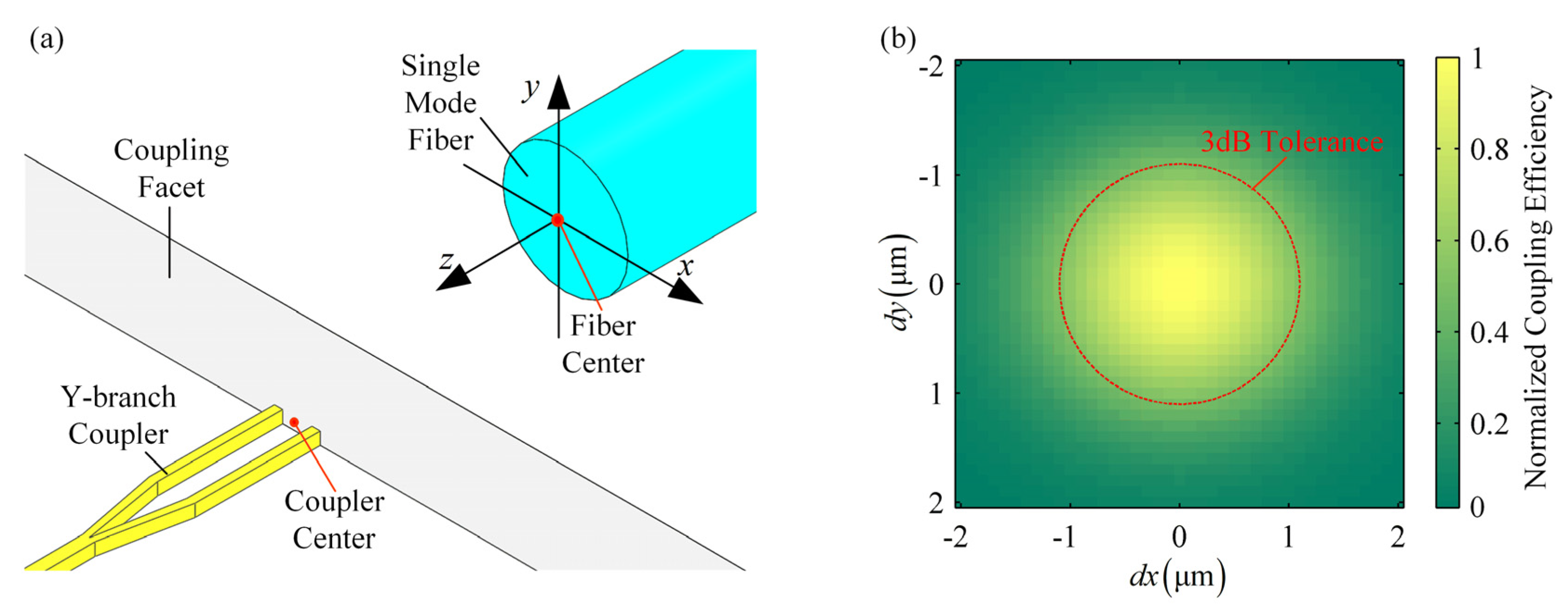
Figure 6a shows the alignment of the SMF and Y-branch coupler. To achieve maximum coupling efficiency, it is necessary to carefully adjust the SMF along the , , and directions, so that SMF center and coupler center can be on the same line and overlapped. In this section, 3 dB alignment tolerance of the Y-branch coupler is analyzed to quantitatively evaluate the difficulty of the alignment.
Figure 6.
(a) Alignment of the single mode fiber (SMF) and waveguide RWS; (b) Influence of the deviation between the SMF center and waveguide center in the plane on the coupling efficiency .
Adjustments in the direction are completed if there is no gap between the SMF and Y-branch coupler. These adjustments are relatively simple, so alignment tolerance in the direction is not analyzed in this paper. Influence of the deviation between the SMF center and coupler center in the plane on the coupling efficiency is shown in Figure 6b. In this figure, denotes the deviation between the SMF center and coupler center in the direction, denotes the deviation in the direction, color bar denotes the normalized coupling efficiency. It is clear to know that the greater the deviation between the SMF center and coupler center is, the lower the coupling efficiency will be. When deviation is outside the red circle, coupling efficiency drops to half of the maximum. Therefore, 3 dB alignment tolerance of the Y-branch coupler is .
3.5. Polarization Dependent Loss of the Y-Branch Coupler
Polarization of mode keeps unchanged if SMF is completely axisymmetric. However, if SMF bends, polarization of mode changes immediately and then coupling efficiency of fiber-to-waveguide coupler changes too [24]. Polarization-dependent loss refers to the decrease in coupling efficiency when mode in the SMF changes from TE mode to TM mode, and it is used to quantitatively evaluate the influence of mode polarization on the coupling efficiency. Polarization-dependent loss can be calculated as follow:
where denotes the coupling efficiency between the SMF and Y-branch coupler when TE mode is in the SMF, denotes the coupling efficiency when TM mode is in the SMF. Coupling efficiency and are 0.24 and 0.13 respectively when width is 0.10 µm, gap is 0.86 µm, and length is 10 µm. Therefore, polarization-dependent loss of the Y-branch coupler () is 0.11.
4. Grating Coupler
Using the grating coupler is also an effective way to improve the coupling efficiency between the single-mode fiber (SMF) and waveguide reference wavefront source (RWS). Different from Y-branch coupler, grating coupler can be placed at any position of the waveguide RWS and edge of the waveguide RWS does not need to be polished. In this section, firstly, structure of the grating coupler is introduced and key parameters that determine the coupling efficiency are optimized. Secondly, 3 dB fabrication tolerance, 3 dB alignment tolerance, and polarization-dependent loss are analyzed, respectively.
4.1. Structure of the Grating Coupler
Figure 7 shows the structure of the grating coupler which is composed of the grating part and taper part. In the grating part, width of the non-etched area is , width of the etched area is , grating period , duty cycle , and width of the grating part is . In the taper part, denotes its length. Height of the grating coupler along the direction is 250 nm, which is consistent with the height of the silicon nitride (SiN) core.
Figure 7.
Structure of the grating coupler. (a) Three-dimensional view; (b) Top view.
Coupling efficiency of the grating coupler () can be calculated as follow:
where denotes the coupling efficiency between the SMF and grating part, denotes the transmission efficiency of the taper part. To improve the coupling efficiency of the grating coupler, parameters in the grating part and taper part must be optimized.
4.2. Parameter Optimization
Parameter optimization of the grating coupler can be divided into two steps. In the first step, parameters in the grating part are optimized. Bragg diffraction equation [25] is firstly used to calculate the initial value of each parameter. Then, each parameter is continuously adjusted from its initial value by using the particle swarm optimization method [26], so that coupling efficiency tends to the maximum. In the second step, width and length are optimized to improve the transmission efficiency .
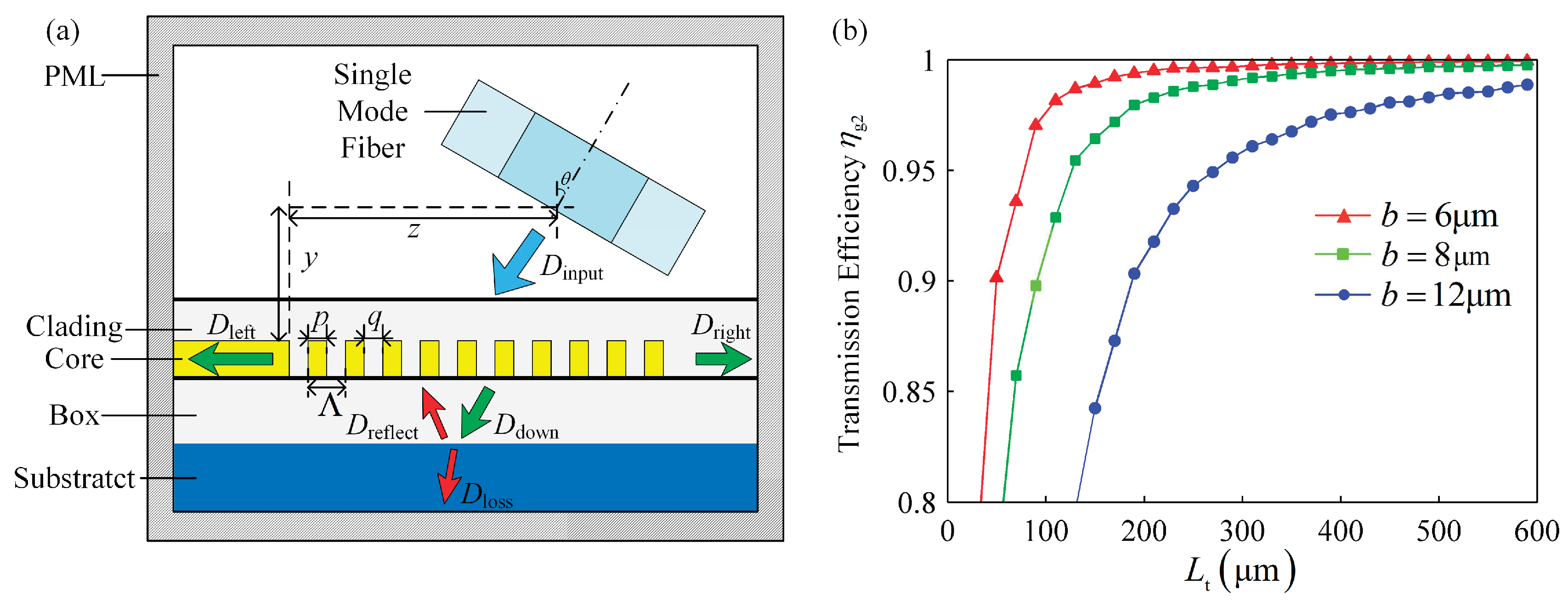
Simulation mode of the grating part is shown in Figure 8a. Since width of the grating part along the direction does not affect the coupling efficiency, two-dimensional finite difference time domain (FDTD) simulation is used which also can greatly save the simulation time and computer memory. In Figure 8a, incident angle denotes the angle between the SMF and normal line, denotes the horizontal distance from the left of the grating to the SMF center, denotes the vertical distance from the top of the grating to the SMF center, arrows denote propagation directions of the lights, PML denotes the perfectly matched layer boundary condition.
Figure 8.
(a) Simulation model of the grating part. (b) Influence of the width and length on the transmission efficiency .
Bragg diffraction equation is given by:
where denotes the refractive index of the grating, denotes the wavelength of the light, denotes the grating period, denotes the diffraction order, denotes the refractive index of the air, denotes the incident angle of the SMF. Initial value of the incident angle is chosen to be to avoid the second-order reflection at the grating. Since initial values of the duty cycle and wavelength are 0.5 and 0.532 µm, respectively, refractive index of the grating can be calculated, and its value is 1.60. According to Equation (6), initial value of the grating period is 0.423 µm when diffraction order is −1. Initial value of each parameter is shown in Table 1.
Table 1.
Parameters of the grating part.
To get the maximum coupling efficiency, four parameters including the grating period , duty cycle , , and are optimized together using the particle swarm optimization method [26]. After 300 iterations, coupling efficiency reaches its maximum of 0.35. The final value of each parameter can also be seen in Table 1. It is worth mentioning that coupling efficiency is polarization sensitive and it gets the maximum when TE mode is in the SMF. Therefore, numerical simulations in the rest of this section use the TE mode.
Transmission efficiency which is determined by the width and length can be calculated as follow:
where denotes the power on the right of the taper part as shown in Figure 7b, denotes the power on the left. Figure 8b shows the transmission efficiency with different width and length . Firstly, with the increase of the length , transmission efficiency continues to improve and tends to be 1. Secondly, when width increases, length should increase at the same time to keep the transmission efficiency constant. Considering the fact that diameter of the mode in the SMF is 3 µm, grating part whose width is 6 µm, is big enough to accept the whole light spot from the SMF because diameter of the mode in the SMF is 3 µm. Once width is chosen to be 6 µm, transmission efficiency of the taper part is nearly close to 1 when length is 300 µm.
In summary, when parameters of the grating part are final values in Table 1, and width and length are 6 µm and 300 µm respectively, coupling efficiency reaches its maximum 0.35, and transmission efficiency is approximately equal to 1. Therefore, maximum coupling efficiency of the grating coupler () is 0.35.
4.3. 3 dB Fabrication Tolerance of the Grating Coupler
To quantitatively evaluate the difficulty of fabricating the grating coupler and to compare it with the difficulty of fabricating the Y-branch coupler, 3 dB fabrication tolerance of the grating period , duty cycle and thickness of the bottom cladding are analyzed.
Effect of the grating period on the coupling efficiency is shown in Figure 9a. Grating period and incident angle must satisfy the Bragg diffraction equation (Equation (6)) to get the maximum coupling efficiency . However, the incident angle remains unchanged in the experiment. This leads to a decrease of the coupling efficiency regardless of the decrease or increase of the grating period . When grating period decreases to 0.40 µm or increases to 0.44 µm, coupling efficiency drops to half of the maximum. Therefore, 3 dB fabrication tolerance of the grating period is −0.02 μm–+0.02 μm.
Figure 9.
(a) Influence of grating period on the coupling efficiency when duty cycle is 0.476. (b) Influence of duty cycle on the coupling efficiency when grating period is 0.42 µm. (c) Influence of bottom cladding thickness on the coupling efficiency .
Figure 9b shows the effect of duty cycle on the coupling efficiency when grating period is 0.420 μm. Coupling efficiency increases first and then decreases with the increase of the duty cycle . Because too large or too small duty cycle enhances the transmission characteristics of the grating and finally leads to the reduction of the coupling efficiency. When duty cycle decreases to 0.36 or increases to 0.60, coupling efficiency drops to half of the maximum. Therefore, 3 dB fabrication tolerance of the duty cycle is −0.12 μm–+0.12 μm. In other words, 3 dB fabrication tolerance of the width or is −0.05 μm–+0.05 μm.
Thickness of the bottom cladding also affects the coupling efficiency . Arrows in Figure 8a clearly show the propagation of the incident light after it enters the grating coupler from the SMF. The light reflected by the substrate (Dreflect) interferes with the light propagating to the waveguide (Dleft), leading to the result that coupling efficiency changes periodically with the increase of the thickness . Figure 9c shows this phenomenon clearly. Coupling efficiency reaches its maximum of 0.35 when thickness is 2.52 μm. Coupling efficiency drops to half of the maximum once thickness decreases to 2.46 μm or increases to 2.58 μm. Therefore, 3 dB fabrication tolerance of the thickness is −0.06 μm–+0.06 μm.
4.4. 3 dB Alignment Tolerance of the Grating Coupler
When aligning the SMF and grating coupler in the experiment, incident angle remains unchanged and position of the SMF is continuously adjusted to get the maximum coupling efficiency. Therefore, only 3 dB alignment tolerance of the and is analyzed.
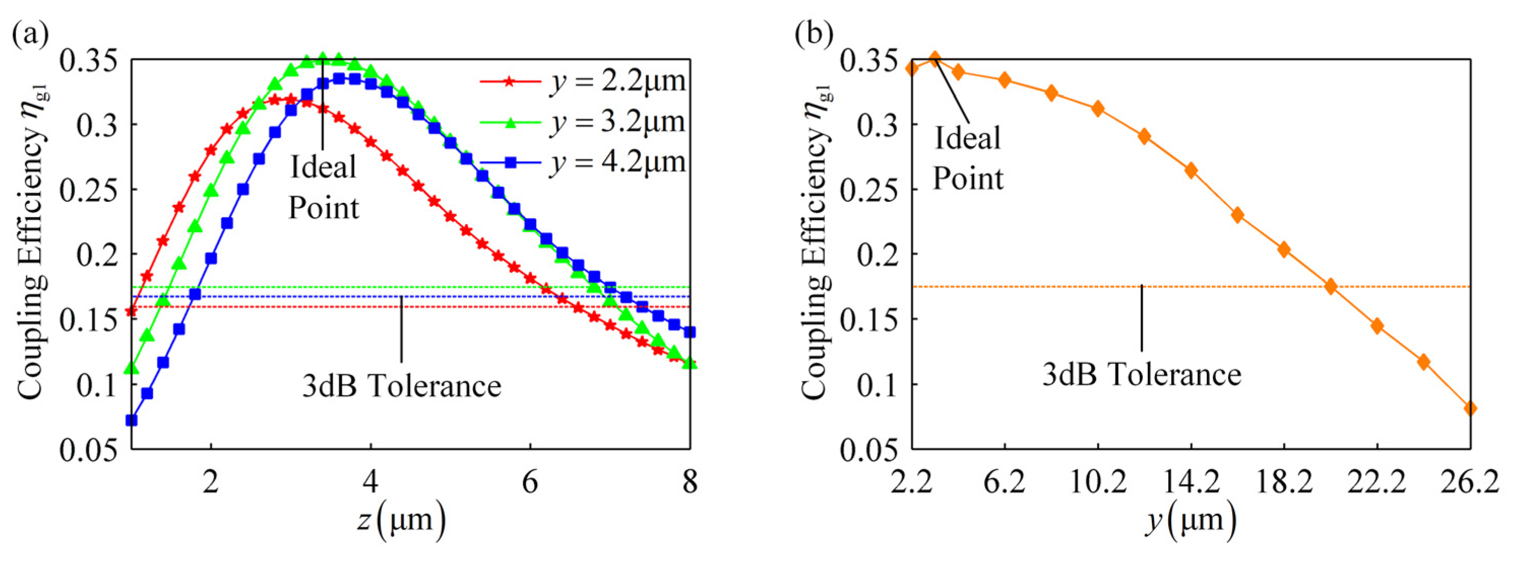
When SMF deviates from the ideal position, effect of the SMF position on the coupling efficiency is shown in Figure 10a. Firstly, with the growth of the , coupling efficiency increases to its maximum and then drops. Secondly, with the growth of the , maximum of the coupling efficiency changes in the same way. When is 3.2 μm, coupling efficiency gets its maximum of 0.35 at z = 3.4 μm and drops to half at z = 1.6 μm or 6.8 μm. Therefore, 3 dB alignment tolerance of the is −1.8 μm–+3.4 μm.
Figure 10.
(a) Influence of the SMF position on the coupling efficiency . (b) Influence of the bottom cladding thickness on the coupling efficiency .
Figure 10b shows the influence of the on the maximum of the coupling efficiency detailly. Coupling efficiency gets its maximum of 0.35 at y = 3.2 μm and drops to half at y = 20.2 μm. Limited by the thickness of the top cladding, the minimum of the is 2 μm. Therefore, 3 dB alignment tolerance of the is −1.2 μm–+12.0 μm.
4.5. Polarization-Dependent Loss of the Grating Coupler
Polarization-dependent loss of the grating coupler () can be calculated as follow:
where denotes the coupling efficiency between the SMF and grating coupler when TE mode is in the SMF, denotes the coupling efficiency when TM mode is in the SMF. Coupling efficiency and are 0.35 and 0.05 respectively when parameters in the grating part are final values in Table 1, width is 6 μm, and length is 300 μm. Therefore, polarization-dependent loss of the grating coupler () is up to 0.30.
5. Comparison of Two Fiber-to-Waveguide Couplers
Table 2 and Table 3 show the parameters, maximum coupling efficiency, 3 dB fabrication tolerance, 3 dB alignment tolerance, and polarization-dependent loss of the Y-branch coupler and grating coupler respectively. Following results can be obtained from two tables, firstly, maximum coupling efficiency of the grating coupler () is greater than Y-branch coupler (). Secondly, in terms of the etching process, difficulty of fabricating the grating coupler is slightly less than that of the Y-branch coupler. When fabricating the Y-branch coupler, minimum size to be etched is 0.10 μm (width ) and its fabrication tolerance is −0.10 μm–+0.05 μm. Minimum size of the grating coupler is 0.20 μm (width ) and its fabrication tolerance is ±0.05 μm. Thirdly, in terms of the coating process, fabricating the Y-branch coupler is easier because thickness of the bottom cladding should be strictly controlled at 2.52 μm and its fabrication tolerance is ±0.06 μm. Fourthly, compared with the Y-branch coupler, it is easier to align the single-mode fiber (SMF) and grating coupler. Because Y-branch coupler must be located at the edge of the waveguide reference wavefront source (RWS), and edge of the waveguide RWS should be polished before using the Y-branch coupler. However, grating coupler does not have this problem. When aligning the SMF and Y-branch coupler, SMF center must be located in a circular area with the radius of 1.10 μm, and center of this circle is Y-branch coupler center. Aligning the SMF with the grating coupler is relatively simpler because of the greater alignment tolerance (−1.8 μm–+3.4 μm along the direction, −1.2 μm–+12.0 μm along the direction). Fifthly, polarization of the mode in the SMF has a great impact on the coupling efficiency no matter for the grating coupler or Y-branch coupler. When mode in the SMF changes from TE mode to TM mode, coupling efficiency of the grating coupler is even reduced by 0.3. Therefore, polarization of the mode in the SMF must be strictly controlled.
Table 2.
Characteristics of the Y-branch coupler.
Table 3.
Characteristics of the grating coupler.
6. Conclusions
In this paper, reference wavefront source (RWS) based on silicon nitride (SiN) waveguide in point diffraction interferometer (PDI) is firstly introduced. Then, maximum coupling efficiency, 3 dB fabrication tolerance, 3 dB alignment tolerance and polarization-dependence loss of the Y-branch coupler and grating coupler are compared to improve the power of wavefront. Simulation results show that waveguide RWS can generate a reference wavefront whose root-mean-square (RMS) value is less than 0.03 nm and numerical aperture (NA) is over 0.5, owing to high refractive index difference between SiN core and silicon dioxide (SiO2) cladding. Using Y-branch coupler or grating coupler is an effective way to improve the power of wavefront. Compared with Y-branch coupler, grating coupler is the more recommended fiber-to-waveguide coupler because its maximum coupling efficiency () is greater. Moreover, etching process and alignment process of grating coupler are easier. Y-branch coupler is a better choice if the coating technology cannot meet the requirement (fabrication tolerance is ±0.06 μm). Finally, polarization of the mode in the single-mode fiber (SMF) must be strictly controlled no matter for grating coupler or Y-branch coupler. This paper improves the power of the wavefront by selecting appropriate fiber-to-waveguide couplers for waveguide RWS. PDI based on the power improved waveguide RWS is expected to be used in many measurement fields.
Author Contributions
Conceptualization, Y.Y., J.B. and Y.C.; methodology, Y.C.; software, Y.C.; validation, Y.C., J.B. and C.W.; formal analysis, Y.C.; investigation, Y.X.; resources, J.B.; data curation, C.W.; writing—original draft preparation, Y.C.; writing—review and editing, Y.Y.; visualization, J.B.; supervision, Y.Y.; project administration, J.B.; funding acquisition, J.B. All authors have read and agreed to the published version of the manuscript.
Funding
This research was supported by National Natural Science Foundation of China (NSFC, grant numbers 61875173, 61627825).
Conflicts of Interest
The authors declare no conflict of interest.
References
- Yang, Y. Advanced Interferometry and Application, 1st ed.; Zhejiang University Press: Hangzhou, China, 2017; pp. 77–89. [Google Scholar]
- Smartt, R.; Steel, W. Theory and application of point-diffraction interferometers. Jpn. J. Appl. Phys. 1975, 14, 351–356. [Google Scholar] [CrossRef]
- Otaki, K.; Ota, K.; Nishiyama, I.; Yamamoto, T.; Fukuda, Y.; Okazaki, S. Development of the point diffraction interferometer for extreme ultraviolet lithography: Design, fabrication, and evaluation. J. Vac. Sci. Technol. B 2002, 20, 2449–2458. [Google Scholar] [CrossRef]
- Li, Y.; Yang, Y.-Y.; Wang, C.; Chen, Y.-K.; Chen, X.-Y. Point diffraction in terference detection technology. Chin. Opt. 2017, 10, 391–414. [Google Scholar] [CrossRef]
- Du, Y.; Feng, G.; Li, H.; Vargas, J.; Zhou, S. Circular common-path point-diffraction interferometer. Opt. Lett. 2012, 37, 3927–3929. [Google Scholar] [CrossRef]
- Zhu, W.; Chen, L.; Gu, C.; Zheng, D.; Cao, H.; Han, Z. Reflective shearing point diffraction interferometer. Microw. Opt. Technol. Lett. 2015, 57, 2845–2848. [Google Scholar] [CrossRef]
- Akondi, V.; Jewel, A.R.; Vohnsen, B. Digital phase-shifting point diffraction interferometer. Opt. Lett. 2014, 39, 1641–1644. [Google Scholar] [CrossRef] [PubMed]
- Wang, D.; Wang, F.; Zou, H.; Zhang, B. Analysis of diffraction wavefront in visible-light point-diffraction interferometer. Appl. Opt. 2013, 52, 7602–7608. [Google Scholar] [CrossRef] [PubMed]
- Shao, W.; Yang, Y.; Chen, X.; Liu, D.; Shen, Y. Optimization research on optical structural parameters of point diffraction interference system. High Power Laser Part Beams 2014, 26, 051001. [Google Scholar] [CrossRef]
- Wang, C.; Yang, Y.; Li, Y.; Chen, Y.; Bai, J. Characterization of the pinhole diffraction based on the waveguide effect in a point diffraction interferometer. Appl. Opt. 2018, 57, 781–787. [Google Scholar] [CrossRef]
- Otaki, K.; Bonneau, F.; Ichihara, Y. Absolute measurement of spherical surface by point diffraction interferometer. Proc. SPIE 1999, 3740, 602–605. [Google Scholar]
- Wang, D.D.; Chen, X.X.; Xu, Y.B.; Wang, F.M.; Kong, M.; Zhao, J.; Zhang, B.W. High-NA fiber point-diffraction interferometer for three-dimensional coordinate measurement. Opt. Express 2014, 22, 25550–25559. [Google Scholar] [CrossRef] [PubMed]
- Mercer, C.R.; Creath, K. Liquid-crystal point-diffraction interferometer. Opt. Lett. 1994, 19, 916–918. [Google Scholar] [CrossRef] [PubMed]
- Millerd, J.E.; Brock, N.J.; Hayes, J.B.; Wyant, J.C. Instantaneous phase-shift, point-diffraction interferometer. In Interferometry XII: Techniques and Analysis; Creath, K., Schmit, J., Eds.; Spie-Int Soc Optical Engineering: Bellingham, WA, USA, 2004; Volume 5531, pp. 264–272. [Google Scholar]
- Sommargren, G.E. Phase Shifting Diffraction Interferometry for Measuring Extreme Ultraviolet Optics. In Proceedings of the Optical Society of America Extreme Ultraviolet Lithography, Boston, MA, USA, 29 April–3 May 1996; pp. 108–112. [Google Scholar]
- Matsuura, T.; Okagaki, S.; Nakamura, T.; Oshikane, Y.; Inoue, H.; Nakano, M.; Kataoka, T. Measurement accuracy in phase-shifting point diffraction interferometer with two optical fibers. Opt. Rev. 2007, 14, 401–405. [Google Scholar] [CrossRef]
- Chkhalo, N.I.; Klimov, A.Y.; Rogov, V.V.; Salashchenko, N.N.; Toropov, M.N. A source of a reference spherical wave based on a single mode optical fiber with a narrowed exit aperture. Rev. Sci. Instrum. 2008, 79, 033107. [Google Scholar] [CrossRef]
- Wang, Q.; He, J.J.; He, S.L. Y-branch spot-size converter for a buried silica waveguide with large index difference. Appl. Opt. 2004, 43, 3315–3318. [Google Scholar] [CrossRef]
- Qian, W.; Jun, L.; Sailing, H. Optimal design method of a low-loss broadband Y branch with a multimode waveguide section. Appl. Opt. 2002, 41, 7644–7649. [Google Scholar]
- Tao, S.H.; Song, J.; Fang, Q.; Yu, M.B.; Lo, G.Q.; Kwong, D.L. Improving coupling efficiency of fiber-waveguide coupling with a double-tip coupler. Opt. Express 2008, 16, 20803–20808. [Google Scholar] [CrossRef]
- Doerr, C.R.; Chen, L.; Chen, Y.-K.; Buhl, L.L. Wide Bandwidth Silicon Nitride Grating Coupler. IEEE Photonics Technol. Lett. 2010, 22, 1461–1463. [Google Scholar] [CrossRef]
- Sacher, W.D.; Huang, Y.; Ding, L.; Taylor, B.J.F.; Jayatilleka, H.; Lo, G.-Q.; Poon, J.K.S. Wide bandwidth and high coupling efficiency Si3N4-on-SOI dual-level grating coupler. Opt. Express 2014, 22, 10938–10947. [Google Scholar] [CrossRef]
- Taillaert, D.; Van Laere, F.; Ayre, M.; Bogaerts, W.; Van Thourhout, D.; Bienstman, P.; Baets, R. Grating couplers for coupling between optical fibers and nanophotonic waveguides. Jpn. J. Appl. Phys 2006, 45, 6071–6077. [Google Scholar] [CrossRef]
- Liao, Y. Characteristics of fiber. In Fiber Optics: Principles and applications, 1st ed.; Zheng, A., Cai, B., Eds.; Tsinghua University Press: Beijing, China, 2003; p. 73. [Google Scholar]
- Chen, H.Y.; Yang, K.C. Design of a high-efficiency grating coupler based on a silicon nitride overlay for silicon-on-insulator waveguides. Appl. Opt. 2010, 49, 6455–6462. [Google Scholar] [CrossRef] [PubMed]
- Bratton, D.; Kennedy, J. Defining a Standard for Particle Swarm Optimization. In IEEE Swarm Intelligence Symposium; IEEE: Piscataway, NJ, USA, 2007. [Google Scholar]
Publisher’s Note: MDPI stays neutral with regard to jurisdictional claims in published maps and institutional affiliations. |
© 2020 by the authors. Licensee MDPI, Basel, Switzerland. This article is an open access article distributed under the terms and conditions of the Creative Commons Attribution (CC BY) license (http://creativecommons.org/licenses/by/4.0/).