Featured Application
This work could initiate a cutting-edge technology that exploits dual applicability of LEDs, i.e., not only for the classical purpose as a luminary, but also for medical radiation detection (diagnostic x-rays).
Abstract
Light-emitting diodes (LEDs) have miscellaneous applications owing to their low cost, small size, flexibility, and commercial availability. Furthermore, LEDs have dual applicability as light emitters and detectors. This study explores the current–voltage (C–V) response of LED strips exposed to diagnostic x-rays. Cold white, warm white, red, green, and blue LED strip colors were tested. Each strip consisted of 12 LED chips and was connected to a multimeter. The variable diagnostic x-ray parameters evaluated were kilovoltage peak (kVp), milliampere-seconds (mAs), and source-to-image distance (SID). The radiation dose was also measured using a dosimeter simultaneously exposed to x-rays perpendicularly incident on the strips. Lastly, the consistency of C–V responses, and any possible degradation after 1–2 months was also analyzed. Each LED strip color was ranked according to its C–V response in each of the investigated parameters. The LED strip color with the best cumulative rank across all the tested parameters was then examined for reproducibility. Our findings revealed that the C–V responses of LED strips are (a) generally low but measurable, (b) inconsistent and fluctuating as a consequence of kVp variations, (c) positively correlated to mAs, (d) negatively correlated to SID, and (e) positively correlated to dose. Overall results suggested cold white LED strip as most feasible for x-ray detection—in comparison to examined colors. Additionally, the reproducibility study using the cold white LED strip found a similar trend of C–V response to all variables except kVp. Outcomes indicate that LED strips have the potential to be exploited for detecting low dose (~0–100 mGy) diagnostic x-rays. However, future studies should be carried out to increase the low C–V signal.
1. Introduction
Radiation measurement and monitoring are some of the vital aspects of medical radiation. In this manner, the exposure of radiation to workers in radiology departments should be continuously monitored. This ensures that the workers’ absorbed radiation doses are kept below the acceptable limits. Likewise, radiation applied during imaging and treatment procedures should be measured routinely to ensure the accuracy of doses delivered to the patients.
Conventional methods in medical radiation measurement include ionization chambers, film badges, electronic dosimeters, and thermal luminescence diodes (TLDs). Current medical radiation measurement methods employ optical material for optically stimulated luminescence (OSL) [1,2] and photonic devices such as photodiodes, photovoltaic sensors, phototransistors, lasers, and cameras (charge-coupled devices, CCDs/complementary metal-oxide-semiconductors, CMOSs). Photonic/optical devices are electronic components specifically utilized for emitting, detecting or manipulating light [3]. Photodiodes have been exploited for diagnostic radiology dosimetry [4,5,6,7] as well as gamma radiation detection and measurement [8,9,10], phototransistors/MOSFETs for gamma-ray detection [11,12] and radiation dosimetry [13,14,15], photovoltaic sensors for medical dosimetry [16,17,18], and CCD/CMOS cameras for Cerenkov luminescence imaging (CLI) in nuclear medicine [19,20,21], radiotherapy [22], and biomedical sciences [23,24].
However, the performance of current photonic devices implemented for radiation measurement deteriorates due to radiation-induced damage/defects [25,26,27,28], leading to photonic device output degradation [29,30,31]. Although a light-emitting diode (LED) can detect electromagnetic (EM) radiation, a lot of research is focused on LED as a luminary—for instance, in phototherapy and photodynamic therapy (PDT) [32,33]. There is limited research about the application of LEDs to the detection of EM radiation. Furthermore, LEDs could demonstrate better radiation hardness compared to other photonic devices such as photodiodes [34,35]. This could imply that when used as radiation detectors, LEDs could withstand higher radiation doses without any degradation in output reading. LEDs are also flexible; they come in the form of surface mount devices (SMD) or chip on board (COB), and are five times cheaper than photodiodes [36].
Connecting current across an LED terminal excites electrons situated in valence bands to conduction bands. During de-excitation, electrons lose their energy and fall back to the valence bands by emitting photons of light energy. To emit a specific color/wavelength, a combination of different elements and materials are used in the fabrication of LEDs.
LEDs are semiconductor devices that consist of a PN junction in their active/sensitive layer [3,37]. Whereas negative charges (electrons) are localized in the N region, positive charges (holes) are in the P region. When EM radiation is incident on a PN junction, electrons absorb packets of EM radiation (photons) and drift to recombine with the holes. Electron drift implies a quantifiable current that could be correlated to the EM radiation incident on the PN junction. In our study, a multimeter connected across the LED terminals displays this current in the form of voltage hence the term current–voltage (C–V) signal is used.
LEDs of different colors are composed of distinct materials and elements. Because a particular wavelength range implies a specific color, in addition to the core PN junction component of the LED active region, phosphor layers are coated on sensitive areas to adjust the emission colors of LEDs [37]. Variation in LED structural components could hence imply a difference in the C–V response of LED strips to x-rays. Thus, our study was conducted to investigate the C–V response of five LED strips (emitting cold white, warm white, red, green and blue respectively) to low dose x-rays of the dosimetric ranges usually used in diagnostic radiology.
2. Materials and Methods
2.1. Apparatus and Experimental Setup
LEDs are solid-state devices and are fabricated using a combination of typical materials/elements to produce different emission wavelengths. For instance, LEDs emitting white light are composed of blue-emitting GaN and a yellow-emitting phosphor [38]. A phosphor is a photoluminescent material that converts short-wavelength light (high energy photons) to long-wavelength light (low energy photons) [37,39]. Table 1 shows some examples of material combinations that are generally used for manufacturing various emission wavelengths of LEDs.

Table 1.
Typical materials and emission wavelengths of light-emitting diodes.
Our experiments were executed using LED strips (12V DC SMD 5050) of five emission colors: cold white, warm white, red, green, and blue. The emission wavelength range for both the cold white and warm white LED strips was ~380–750 nm. Red, green, and blue LED strip emission wavelength ranges were ~630–640, 520–530, and 430–470 nm respectively.
LED strips are manufactured by soldering discrete LED chips on a conducting strip. This strip comprises other electronic components such as resistors. In our study, this strip was 1 cm wide, 0.2 cm thick, 500 cm long, and it consisted of 60 LED chips per meter, hence 5 m had 300 LED chips. On the strip, each LED chip was positioned at a 12 mm interval and its active area was of a diameter of approximately 4 mm. The strip was also cuttable at a junction of every three chips and its base was self-adhesive. As a luminary, the strip operated under a 12-volt potential difference across its terminals. Such an LED strip is called an SMD (Figure 1).
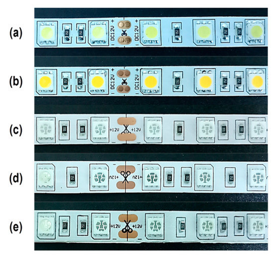
Figure 1.
Images of (a) cold white, (b) warm white, (c) red, (d) green, and (e) blue light-emitting diode (LED) strips.
In this experiment, the LED strips were exposed to x-ray beams from an x-ray generator (Optimus 80, Philips). The beams originated from a broad focal spot (1.0 mm) and were perpendicularly incident on all LED chip sensitive areas and the dosimeter probe. The x-ray generator is controlled by microprocessors and consists of a control panel, a high voltage generator, and an automatic exposure control (AEC) device. All these generator components are housed in a standard casing. The generator’s non-AEC setting ranges for radiography are as follows: tube voltage (kVp), 40–150 kV; tube current, 1–1100 mA; tube current-time product (mAs), 0.5–850 mAs; and exposure time range, 1–6000 ms.
Exposure of the LED chips to x-ray photons instantly resulted in a radiation-induced current flow in the strips. A multimeter connected to the strips measured the potential difference, a result of the radiation-induced current flow. Therefore, in our study, the obtained signal was referred to as a current–voltage (C–V) signal. The multimeter used in this study was a handheld and multi-functional digital multimeter/oscilloscope (Model JDS2012A, Jinhan Company: Hefei, Anhui, China). This model has a single channel and functions as both a digital oscilloscope (with a 200 MSa/s maximum sampling rate and bandwidth 20MHz) and as a multimeter (4000 counts). It can measure DC/AC voltages, resistance, and capacitance, and it can test diodes and continuity.
The dose of the x-rays incident on the LED strip was recorded using an easy-to-use pocket-sized radiation dosimeter (Unfors Xi, RaySafe). This dosimeter consists of two parts—a base unit which displays all measured parameters in three rows of alphanumeric characters, and a sensitive detector/probe which is capable of measuring kVp, dose, dose rate, pulses, dose per pulse, time, and waveforms for all x-ray machines. The dosimeter probe and strip were placed adjacent to the x-ray beam’s central axis and perpendicularly irradiated while on top of two polystyrene blocks as seen in Figure 2. Because the x-ray tube has a pre-collimator copper filter, the x-ray beam was considered to be homogenous. Therefore, the x-ray photons incident on both the dosimeter probe and LED strips were of identical average energies.
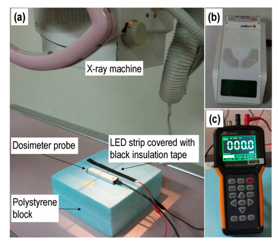
Figure 2.
(a) Experimental setup for measuring the current–voltage (C–V) signal response and diagnostic x-ray dose. Each tested LED strip contained 12 LED chips which were connected in parallel by the manufacturer. The strip was positioned on the beam’s central axis to minimize x-ray flux inhomogeneity dependency that arises due to the heel effect. (b) Unfors base unit that is connected to a detector/probe with a detachable cable. (c) Handheld digital multimeter connected to an LED strip for taking radiation-induced signal readings.
2.2. Irradiation and Exposure Settings
While the x-ray generator was in the non-AEC mode, the strips were irradiated in three exposure sets. In each exposure set, only one of the kVp, mAs, and surface-image-distance (SID) parameters was varied as shown in Table 2. The kVp, mAs and SID values are x-ray tube parameter settings usually adjusted to acquire an optimum quality of radiographs in diagnostic radiology, while ensuring minimum radiation exposure to patients. Kilovoltage peak (kVp) is a high voltage (in kV) applied between the anode and the cathode of the tube to accelerate electrons. The kVp value is directly proportional to the energy of the x-ray photons in the beam [41]. Milliamperage second (mAs) is a small current (mA) and time (s) product. Milliamperage is the low current (in mA) that flows in the tube’s tungsten cathode filament and hence consists in thermionically emitting electrons [42]. The time (s) is the x-ray beam exposure time. The mAs value is therefore directly proportional to the number of x-ray photons in the x-ray beam. Source-to-image distance (SID) is the distance between the image receptor (detector) and the tube’s x-ray source point. The SID is inversely proportional to the radiation exposure of the dosimeter probe/strips–if the kVp and mAs are kept constant i.e., shorter SIDs imply more exposure of the dosimeter probe/strips to radiation, and longer SIDs imply less exposure. In our study, the kVp, mAs, and SID parameter settings (values) for each exposure were referenced from Sezdi’s work [43].
Table 2.
The settings of kVp, mAs, and SID in each exposure.
In the first exposure set, the mAs and SID were constant at 50 and 60 cm respectively. Readings were then obtained when the tube voltage was varied from 40 to 117 kVp. Similarly, in the second exposure set, the kVp and SID values were constant at 70 and 60 cm respectively. Readings were then taken when the tube current–time product was adjusted from 0.5 to 250 mAs. In the last exposure set, while maintaining the mAs and kVp at 50 and 70 respectively, readings were taken when the SID range was 30–100 cm, as illustrated in Table 2.
3. Results and Discussion
3.1. C–V Response to kVp
Generally, the LED strip signal C–V response to kVp fluctuated across all the LED strip colors. For the cold white, warm white, and red LED strip colors, signal increments of 0.1, 0.1 and 0.3 mV were observed when the kVp was increased from 40 to 117. On the contrary, the blue LED strip’s signal decreases from 0.3 mV at a kVp of 40 to 0.1mV at the kVp of 117. Although the green LED strip signal initially increases by 0.3 mV as the kVp is increased from 40 to 80, it decreases to 0 when the kVp is further increased to 117—as seen in Figure 3.
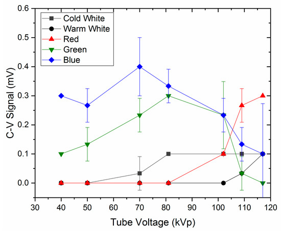
Figure 3.
The C–V responses of cold white, warm white, red, green, and blue LED strips to the kilovoltage peak (kVp) parameter variations.
EM radiation such as light is a wave and a particle simultaneously. When radiation is incident on a PN junction, interactions between radiation photons and PN junction particles/electrons occur. These interaction mechanisms include photoelectric effect, Compton scattering, pair production, coherent scattering, and bremsstrahlung radiation emission. However, the incident photon energy dictates the interaction mechanism, for instance, energies < 100 keV give rise to the photoelectric effect, energies from 100 keV to 10 MeV produce Compton scattering, and energies > 1 MeV cause pair production [44]. For low energy photons, the photoelectric effect is dominant whereas Compton scattering is dominant for high-energy photons [45,46]. Low energy photons could also stimulate coherent scattering and this occurs when the incident photon energies are less than 10 keV [47,48]. However, coherent scattering takes place in high atomic number elements [48]. Because semiconductor PN junctions are not made of high atomic number elements, coherent scattering would be non-existent in the LED strip’s structure.
Electron-hole combinations in LED strips are as a result of mainly the photoelectric effect and Compton scattering. This simultaneous contribution of the photoelectric effect and Compton scattering to radiation-induced current could be a possible explanation for the inconsistent graphs in Figure 3; kVp alters the energy of the incident photons [41]. In other words, kVp changes the beam quality similar to the half-value layer (HVL) [49]. Additionally, post-Compton scattering photons could similarly excite electrons in the form of impact ionization [50]. In Oliveira’s study [6], photodiode signals of four different brands were also inconsistent when the incident photon energy was varied [6].
Modification of LEDs to emit colored light involves altering the structural composition of LEDs. For instance, phosphors could be added. Even though identical x-ray photons are considered to be striking all the LED strips, the different graphs observed in Figure 3—across all the LED strips—could also be a result of the variation in the material composition of the strips. X-ray tube beam filters ensure beam homogeneity by blocking low energy photons (scattered photons), and allowing photons surpassing a specific level of energy to pass through. Nonetheless, photons in an x-ray beam could still be heterogeneous. This could also be a possible explanation for the fluctuated LED strip C–V response observed in Figure 3.
3.2. C–V Response to mAs
In general, for all the strips used in this study, the C–V signal was linear to mAs variation. The green C–V signal data points were very close to the linear fit hence had the highest R-squared value—0.9784. The R-squared values for the cold white, warm white, red, and blue were 0.9673, 0.6199, 0.9775, and 0.8282 respectively, as observed in Figure 4. Higher R-square values implied higher conformity of the signal data points to the linear fit. This further indicated that the signal linearly increased as the mAs was increased. The magnitude and rate at which the signal increases is however depicted by the linear fit’s slope. The slopes for the cold white, warm white, red, green, and blue C–V graphs were 0.0015, 0.0004, 0.0022, 0.0015, and 0.0011 respectively. The red LED strip had the highest signal increment per unit mAs, i.e., 0.0022 mV per unit increase in mAs. Conversely, the warm white had the lowest signal increment per unit mAs, i.e., 0.0004 mV per unit increase in mAs. In all LED strip colors tested, a threshold effect was observed for all tube current values below 20 mAs. No signal is observed for these tube current-time product values (as illustrated in Figure 4).
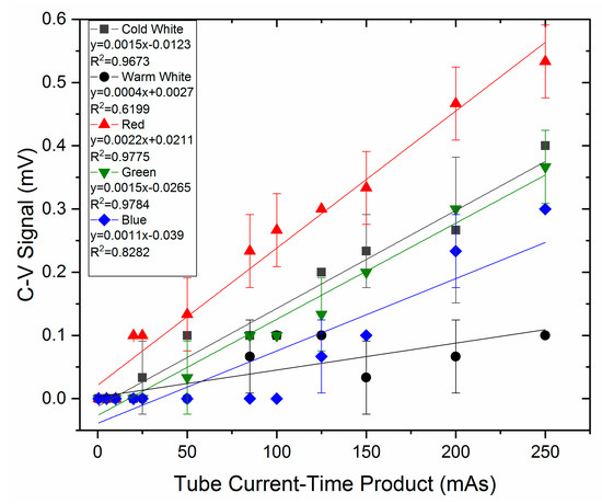
Figure 4.
The C–V responses of cold white, warm white, red, green, blue LED strips to the milliamperage (mAs) parameter alteration.
The tube current-time product (mAs) is correlated to the quantity of thermionically emitted electrons in the x-ray tube [42]. This corresponds to the number of x-ray photons in the x-ray beam i.e., x-ray beam population. In our study, maintaining a constant kVp (incident photon energy) while varying the mAs (number of photons) produced more linear signals. Therefore, the LED strip C–V response was more sensitive and linear to the number of photons in the x-ray beam (mAs). In other words, the charge drift in LED strip PN junctions was linear to the number of photons in the x-ray beam. The charge drift’s linear dependency on x-ray beam photon number thus implies a specific quantity of x-ray photons correspondingly excites a discrete number of electrons resulting in a fixed amount of radiation-induced C–V signal. The threshold effect observed across the LED strips could further imply the minimum quantity of x-ray photons that has to be present in the x-ray beams before charge drift/electron excitation takes place. Tugwell’s findings [51] coincide with ours since our output signal was linear to the tube current (mAs); thus, radiation dose is linear to the tube current (mAs) and tube potential (kVp) [52,53].
3.3. C–V Response to SID
The LED strip C–V signals predominantly decreased due to an increase in the SID. Increasing the SID from 30–100 cm corresponded to a signal reduction of the cold white, warm white, red, and green LED strips. However, the blue LED strip signal fluctuated and slightly increased as a result of increasing the SID. The signal decrease for the cold white, warm white, red, and green LED strips obeyed the inverse square law. This was because the signal data points conformed to exponential decay fits. The cold white, warm white, red, and green LED strips’ R-squared values were 0.9946, 0.8367, 0.8935, and 0.7524 respectively.
Air consists of nitrogen, oxygen, argon, carbon dioxide, and other gases. This implies that air contains charged particles like electrons in the gaseous atoms and molecules. Therefore, when x-rays travel through the air, interactions like Compton scattering and the photoelectric effect may occur, and this would reduce the beam’s final/total energy. Therefore, increasing the SID implies increasing the volume of the gaseous/charged particles interacting with the beam. From Figure 5, it is evident that the C–V signal is an exponential function of SID. This exponential function conforms to the inverse square law (1/r2). In other terms, the C–V signal varies as an inverse square of the SID. On average, shorter SIDs yielded higher signals than longer SIDs for all LED strip colors. At shorter SIDs, photons lose less energy along their trajectories (from the x-ray beam source point to the LED strip active area) and hence deposit higher energy to the electrons—resulting in a high C–V signal. On the contrary, photons lose most of their energy to charges in air (during longer SID trajectories) hence low C–V signals. Similarly, Tugwell [51] observed a negative correlation between dose and SID. The effective and entrance surface doses reduced with an increment in the SID [51].
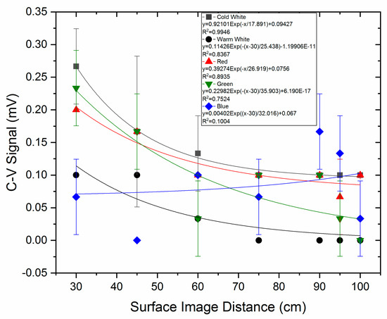
Figure 5.
The C–V responses of cold white, warm white, red, green, and blue LED strips to the SID parameter alteration.
3.4. C–V Response to Dose
There was a high linear correlation between all the LED strip C–V signals and dose. The C–V signals were collected during varied mAs whilst maintaining constant kVp and SID values. This setting was in correspondence with the standard linearity quality control test protocol. C–V signal data points highly conformed to the linear fits based on the R-square values. The cold white, warm white, red, green, and blue LED strip determination coefficients (R-squared values) were 0.9693, 0.6132, 0.9773, 0.9470, and 0.8234 respectively. Sensitivity coefficients for the cold white, warm white, red, green, and blue LED strips were 0.0123, 0.0038, 0.0181, 0.0133 and 0.0095 mV/mGy respectively. Therefore, as in Figure 6, the red LED strip had the highest sensitivity to dose. On the other hand, warm white had the least sensitivity to dose.
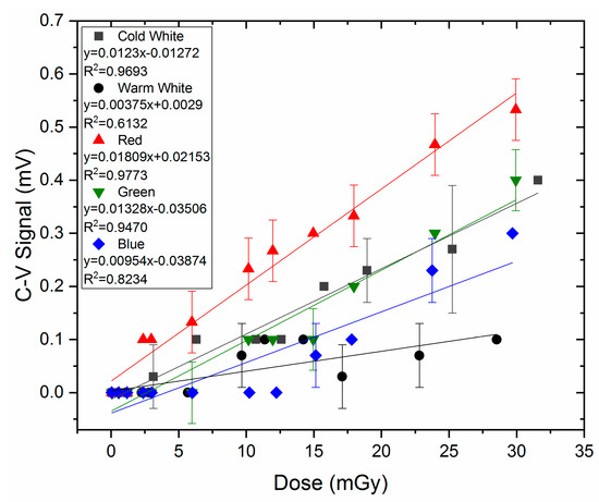
Figure 6.
The C–V responses of cold white, warm white, red, green, blue LED strips to x-ray doses during varied mAs, and fixed kVp and SID.
Similar to Paschoal’s study [5], where the photodiode and phototransistor dosimetric parameter (collected charge) was evaluated for its linearity to dose, the C–V response linearity to absorbed dose was assessed. Absorbed dose is the energy deposited in a unit of mass by ionizing radiation (J/kg-Gy). LED strip C–V signal linearity to absorbed dose thus implies x-ray beam photons imparted their energy in the active area region of the LED strips. Consequently, energy linearly lost by the x-ray photons to the PN junction electrons induced charge drifts and eventually C–V signals.
LED strips are a promising dosimetric tool because their signal increases in accordance with the absorbed dose of ionizing radiation measured by a standard dosimeter. Standard electronic dosimeters similarly produce electronic signals that are converted (calibrated) and displayed to inform of radiation dose in the dosimeter reader unit.
3.5. Consistency of C–V Response
Three signal readings were taken to investigate the consistency of the C–V signal reading for all the five strips tested in this study. These signals were consecutive, and they were recorded at the same mAs value as seen in Figure 7. Consistent signals were obtained at 50, 85, 100, 125, and 250 mAs for the cold white strip; 100, 125, 250 mAs for the warm white strip; 20, 25, and 125 mAs for the red strip; 85, 100, 150 and 200 mAs for the green strip; and 150 and 250 mAs for the blue strip. Therefore, the cold white strip had the highest number of consistent signals at different mAs values: 50, 85, 100, 125, and 250, a total of five. On the other hand, the blue LED’s signals were consistent at only two mAs values: 150 and 250. In some readings, there was no signal detected hence one or two bars are observed.
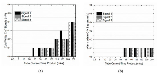
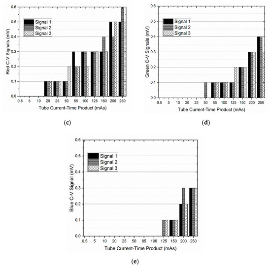
Figure 7.
Stability of three C–V signal measurements of (a) cold white, (b) warm white, (c) red, (d) green, and (e) blue LED strips during the mAs parameter variation.
The slight signal fluctuations observed in Figure 7 could be attributed to radiation-induced trapping effects [27]. Signal 1 could be low due to electrons being immobile in deep traps, and signals 2 and 3 could be high due to excitation of electrons out of the deep traps. Deep traps are located between valence and conduction energy bands [1,27]. PN junction localized electrons may be propelled into these deep traps after absorbing a high amount of energy from the x-ray photons. As a consequence of charge trapping, charges are immobile hence lower radiation-induced excitations. However, absorption of x-ray photon energy by the trapped charge could free them from being interlocked in deep traps. Thus, higher signals would be observed in subsequent C–V response measurements. This phenomenon could, therefore, be a possible explanation for the slight signal fluctuations observed in Figure 7. Connecting a higher operating current to the LEDs for luminescence could be an annealing technique that would improve this signal fluctuation effect [34].
3.6. Degradation of C–V Response
Slight degradations in the C–V response for the cold white LED strip was observed at mAs values of 125, 150, and 250. There was also warm white LED strip signal decrease during the 85, 100, and 125 mAs exposures. The red LED strip signal also decreased when the mAs values were 20, 25, 50, 85, 100, 125, 150, 200, and 250. However, minimal signal depletions were observed during the 200 and 250 mAs exposure settings for both the green and blue LED strips as observed in Figure 8. The cold white LED strip’s signal stability was observed at three mAs values: 50, 85, and 100. Similarly, the green LED strip signal was steady during the 85 and 125 mAs exposure settings. The warm white LED strip signal stability was only during the 250 mAs setting. Contrarily, the red and blue LED strip signals were unstable for all the tested mAs settings. Therefore, overall, the cold white LED strip had the highest number of steady and smallest number of degraded signals at different mAs exposure settings. Nevertheless, the red LED strip had the least stable and most degraded signals. Therefore, the cold white LED strip is preferred since output signal stability is an essential factor for a prospective radiation detector [5].
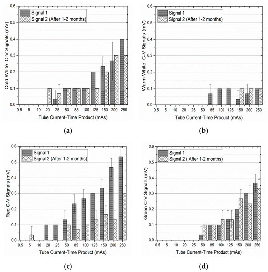
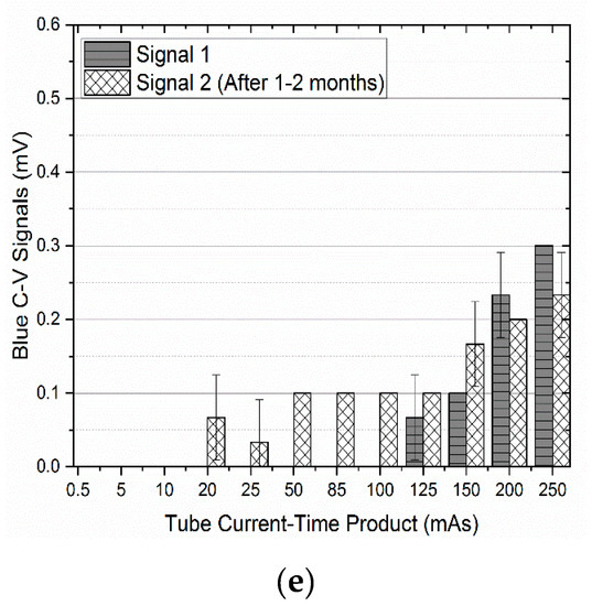
Figure 8.
C–V signal against mAs graphs of (a) cold white, (b) warm white, (c) red, (d) green, and (e) blue LED strips showing any possible C–V response deteriorations as a result of radiation exposure.
Bombardments during Compton scattering and photoelectric effects could displace charge (electrons) from their original lattice structural locations [26,54]. This results in the absence of electrons in their normal lattice positions (vacancies) and electrons occupying lattice positions where they are not meant to be (interstitials) [54]. When an x-ray photon deposits its energy to a vacancy or an interstitial, low/no charge excitation will occur thus low/no C–V signals. Therefore, LED strip C–V signal decrease was perhaps a result of these radiation-induced displacement effects. Post-irradiation signal degradation was also observed in other studies [10,30]. In these studies, LEDs and photodiodes were used. A possible solution to output degradation would be annealing the LEDs to “flush out” the vacancies and interstitials. During the annealing process, both the vacancies and interstitials recombine as suggested by Beringer [34].
3.7. Determination of the Optimum LED Strip Colour
In Table 3, the LED strip color with the best C–V response results was examined based on the individual color rankings for each investigated parameter. For instance, the red LED strip was ranked first in the C–V response to dose because its signal had the highest linearity to dose. Cold white emerged with the lowest cumulative rank, i.e., 10/30, and hence ranked first. On the other hand, blue was ranked last because it had a cumulative rank of 25/30. Therefore, cold white was nominated for the reproducibility test.
Table 3.
Ranking of LED strips based on C–V response.
3.8. Reproducibility Using Cold White LED Strip
Figure 9 includes graphical illustrations of the C–V signal dependency on kVp, mAs, SID, and dose for the cold white LED strip in the reproducibility examination. The C–V signal had a high linear dependency on the peak kilovoltage, all the data points were on the regression line. Therefore, there was a 99.76% linearity correspondence between the signal and the tube voltage. A signal increase of 0.0034 mV was observed per unit increase in the kVp.
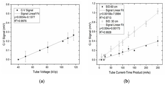
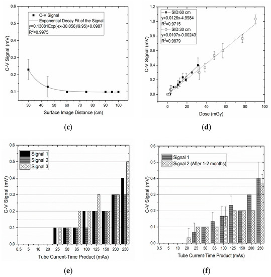
Figure 9.
C–V signal reproducibility graphs based on (a) kVp, (b) mAs, (c) SID, (d) dose, (e) consistency, and (f) degradation variations.
Similarly, the cold white C–V strip signal response to the current-time product (mAs) variation was remarkably linear: The R-squared values were 0.9713 and 0.9928 for SIDs of 60 and 30 cm respectively. Further, the linear fit for the C–V signal obtained at 30 cm SID had a higher increase in magnitude per unit increase in mAs—in comparison to the C–V signal obtained at 60 cm SID. The C–V signal as a function of SID was in the form of an exponential decay with a determinant coefficient of 0.9975. The C–V signal, in other words, decreased as a reverse square of the SID. The strip’s C–V signal was also appreciably linearly dose-dependent with R-squared values of 0.9715 at 60 cm SID and 0.9879 at 30 cm SID. LED strip sensitivity to dose was highly independent of SID variation, i.e., the sensitivities at 60 cm SID (0.0126 mV/mGy), and 30 cm SID (0.0107 mV/mGy) had a 15 % disparity. In other words, LED sensitivity was 85 % similar at the 60 cm and 30 cm SIDs. Additionally, the strip’s signal was consistent; consecutively measured signals 1, 2, and 3 were equivalent at 50, 150, and 200 mAs settings. Signal degradation due to radiation exposure was trivial for the 85, 125, and 250 mAs exposure setting. No signal degradation was observed for the 50, 100, and 150 mAs values.
In the reproducibility investigation, the cold white LED strip was preferred because its C–V response to dose was outstanding among the tested LED strip colors. Further, the C–V signal was substantially reproducible, the least degraded, and the most consistent in comparison to other tested colors. The cold white C–V signal response to kVp, mAs and SID was also steady when compared to other LED strips colors. Likewise, in a study by Oliveira [6] that evaluated four commercial photodiodes for radiology dosimetry, the BPW34 photodiode was nominated to execute radiation-induced current measurements based on its reproducibility and repeatability.
It is observed that graphs from Section 3.1 through 3.8 have noticeable statistical errors. This could be on account of the stability of the x-ray tube and LED chips, and the thickness of the depletion region (LED active area). Owing to variation of photon fluence striking the LED active area (under different SIDs) and the random interaction of x-ray photons, it remains questionable whether all the incident x-ray photons deposited within the depletion region create electrons which are then detected as C–V signals. This could also be a possible source of statistical errors in the graphs.
4. Conclusions
This work explored diagnostic x-ray-induced signals in the form of C–V response using LED strips. This was because SMD LEDs are flexible, low-cost, and commercially available. Cold white, warm white, red, green, and blue LED strip colors were benchmarked and ranked according to the C–V signal response to kVp, mAs, SID, and dose. Further, desirable dosimetric characteristics such as high reproducibility and low degradation due to radiation exposures were evaluated. Results suggested cold white as the most feasible color for diagnostic x-ray radiation detection and measurement. However, LEDs have low sensitivity towards diagnostic x-rays thus the obtained C–V signal was of low magnitude (0–1.1 mV). Therefore, future studies could focus on LED C–V signal amplification. LED annealing techniques (by luminescence) could also be applied to reduce the slight signal degradation and C–V signal fluctuation effects. In our study, cold white LED strips demonstrated the potential to detecting low dose (~0–100 mGy) diagnostic x-rays.
Author Contributions
Conceptualization, M.N.S.Y.; data curation, E.D. and M.N.S.Y.; formal analysis, E.D. and M.N.S.Y.; funding acquisition, M.N.S.Y.; investigation, S.S., N.F.H.Z., N.A.Z., N.S.A.S., M.A.Z. and N.k.Y.A.; methodology, M.N.S.Y.; project administration, M.N.S.Y.; resources, M.N.S.Y.; supervision, M.N.S.Y., A.F.O. and N.H.M.T.; validation, E.D. and M.N.S.Y.; visualization, E.D.; writing—original draft, E.D. and M.N.S.Y.; writing—review & editing, E.D., M.N.S.Y., A.F.O. and N.H.M.T. All authors have read and agreed to the published version of the manuscript.
Funding
This work was supported by the Short-Term Grant, Universiti Sains Malaysia (USM) [grant number: 304/PPSK/6315117].
Acknowledgments
The authors would like to thank the Department of Radiology, Hospital Universiti Sains Malaysia (HUSM) for giving the permission to use the x-ray equipment and providing necessary technical resources during the experiments.
Conflicts of Interest
The authors declare no conflict of interest.
References
- Yukihara, E.; McKeever, S. Optically stimulated luminescence (OSL) dosimetry in medicine. Phys. Med. Biol. 2008, 53, R351. [Google Scholar] [CrossRef] [PubMed]
- Nascimento, L.; Vanhavere, F.; Boogers, E.; Vandecasteele, J.; De Deene, Y. Medical dosimetry using a RL/OSL prototype. Radiat. Meas. 2014, 71, 359–363. [Google Scholar] [CrossRef]
- Damulira, E.; Yusoff, M.N.S.; Omar, A.F.; Taib, M.; Hartini, N. A Review: Photonic Devices Used for Dosimetry in Medical Radiation. Sensors 2019, 19, 2226. [Google Scholar] [CrossRef] [PubMed]
- Romei, C.; Di Fulvio, A.; Traino, C.A.; Ciolini, R.; d’Errico, F. Characterization of a low-cost PIN photodiode for dosimetry in diagnostic radiology. Phys. Med. 2015, 31, 112–116. [Google Scholar] [CrossRef]
- Paschoal, C.; Souza, D.D.N.; Santo, L. Characterization of three photo detector types for computed tomography dosimetry. World Acad. Sci. Eng. Technol. 2011, 56, 92–95. [Google Scholar] [CrossRef]
- Oliveira, C.N.; Khoury, H.J.; Santos, E.J. PiN photodiode performance comparison for dosimetry in radiology applications. Phys. Med. 2016, 32, 1495–1501. [Google Scholar] [CrossRef]
- Nazififard, M.; Suh, K.Y.; Mahmoudieh, A. Experimental analysis of a novel and low-cost pin photodiode dosimetry system for diagnostic radiology. Rev. Sci. Instrum. 2016, 87, 073502. [Google Scholar] [CrossRef]
- Kainka, B. Measure Gamma Rays with a Photodiode. Radiat. Detect. Using BPW34//Elektor Mag. 2011, 6, 22–26. Available online: https://pdfs.semanticscholar.org/9690/cf9481cbc75c1d920c5e9038a9940dd73c66.pdf (accessed on 26 December 2019).
- Oliver, S.M. Silicon Photodiodes for Gamma Ray Detection: First Sensor 2011. Available online: https://www.first-sensor.com/cms/upload/datasheets/gamma-ray-detection.pdf (accessed on 26 December 2019).
- Anđelković, M.S.; Ristić, G.S. Feasibility study of a current mode gamma radiation dosimeter based on a commercial PIN photodiode and a custom made auto-ranging electrometer. Nucl. Technol. Radiat. Prot. 2013, 28, 73–83. [Google Scholar] [CrossRef]
- Andjelković, M.S.; Ristić, G.S. Current mode response of phototransistors to gamma radiation. Radiat. Meas. 2015, 75, 29–38. [Google Scholar] [CrossRef]
- Pejovic, M.M. Application of p-channel power VDMOSFET as a high radiation doses sensor. IEEE Trans. Nucl. Sci. 2015, 62, 1905–1910. [Google Scholar] [CrossRef]
- Santos, L.A.; Araujo, G.G.; Oliveira, F.L.; Silva, E.F., Jr.; Santos, M.A. An alternative method for using bipolar junction transistors as a radiation dosimetry detector in breast cancer treatment. Radiat. Meas. 2014, 71, 407–411. [Google Scholar] [CrossRef]
- Dybek, M.; Kozłowska, B. Evaluation of the applicability of MOSFET detectors in radiotherapy. Radiat. Meas. 2014, 71, 412–415. [Google Scholar] [CrossRef]
- Andjelković, M.S.; Ristić, G.S.; Jakšić, A.B. Using RADFET for the real-time measurement of gamma radiation dose rate. Meas. Sci. Technol. 2015, 26, 025004. [Google Scholar] [CrossRef]
- Hofstetter, M.; Howgate, J.; Sharp, I.D.; Stutzmann, M.; Thalhammer, S. Development and evaluation of gallium nitride-based thin films for x-ray dosimetry. Phys. Med. Biol. 2011, 56, 3215. [Google Scholar] [CrossRef]
- Diab, H.; Ibrahim, A.; El-Mallawany, R. Silicon solar cells as a gamma ray dosimeter. Measurement 2013, 46, 3635–3639. [Google Scholar] [CrossRef]
- Zygmanski, P.; Abkai, C.; Han, Z.; Shulevich, Y.; Menichelli, D.; Hesser, J. Low-cost flexible thin-film detector for medical dosimetry applications. J. Appl. Clin. Med. Phys. 2014, 15, 311–326. [Google Scholar] [CrossRef]
- Chin, P.T.; Welling, M.M.; Meskers, S.C.; Olmos, R.A.V.; Tanke, H.; van Leeuwen, F.W. Optical imaging as an expansion of nuclear medicine: Cerenkov-based luminescence vs fluorescence-based luminescence. Eur. J. Nucl. Med. Mol. Imaging 2013, 40, 1283–1291. [Google Scholar] [CrossRef]
- Robertson, R.; Germanos, M.S.; Li, C.; Mitchell, G.S.; Cherry, S.R.; Silva, M.D. Optical imaging of Cerenkov light generation from positron-emitting radiotracers. Phys. Med. Biol. 2009, 54, N355. [Google Scholar] [CrossRef]
- Nordstrom, R.; Cherry, S.; Azhdarinia, A.; Sevick-Muraca, E.; Van Brocklin, H. Photons across medicine: Relating optical and nuclear imaging. Biomed. Opt. Express 2013, 4, 2751–2762. [Google Scholar] [CrossRef]
- Roussakis, Y.; Zhang, R.; Heyes, G.; Webster, G.; Mason, S.; Green, S.; Pogue, B.; Dehghani, H. Real-time Cherenkov emission portal imaging during CyberKnife® radiotherapy. Phys. Med. Biol. 2015, 60, N419. [Google Scholar] [CrossRef] [PubMed]
- Ciarrocchi, E.; Belcari, N. Cerenkov luminescence imaging: Physics principles and potential applications in biomedical sciences. EJNMMI Phys. 2017, 4, 14. [Google Scholar] [CrossRef] [PubMed]
- Tanha, K.; Pashazadeh, A.M.; Pogue, B.W. Review of biomedical Čerenkov luminescence imaging applications. Biomed. Opt. Express 2015, 6, 3053–3065. [Google Scholar] [CrossRef] [PubMed]
- Johnston, A.H. Proton displacement damage in light-emitting and laser diodes. IEEE Trans. Nucl. Sci. 2001, 48, 1713–1720. [Google Scholar] [CrossRef]
- Omar, N.I.C.; Hasbullah, N.F.; Rashid, N.K.A.M.; Abdullah, J. Electrical properties of neutron-irradiated silicon and GaAs commercial diodes. In Proceedings of the 2012 IEEE Symposium on Industrial Electronics and Applications (ISIEA), Bandung, Indonesia, 23–26 September 2012. [Google Scholar] [CrossRef]
- Omar, N.I.C.; Hasbullah, N.F.; Rashid, N.K.A.M.; Abdullah, J. Effects on electrical characteristics of commercially available Si and GaAs diodes exposed to californium-252 radiation. In Proceedings of the 2012 International Conference on Computer and Communication Engineering (ICCCE), Kuala Lumpur, Malaysia, 3–5 July 2012. [Google Scholar] [CrossRef]
- Ali, K.; Khan, S.A.; MatJafri, M. 60Co γ-irradiation effects on electrical characteristics of monocrystalline silicon solar cell. Int. J. Electrochem. Sci. 2013, 8, 7831–7841. Available online: http://www.electrochemsci.org/papers/vol8/80607831.pdf (accessed on 26 December 2019).
- Lischka, H.; Henschel, H.; Kohn, O.; Lennartz, W.; Schmidt, H. Radiation effects in light emitting diodes, laser diodes, photodiodes, and optocouplers. In Proceedings of the RADECS 93, Second European Conference on Radiation and its Effects on Components and Systems, Saint Malo, France, 13–16 September 1993. [Google Scholar] [CrossRef]
- Orlova, K.; Gradoboev, A.; Asanov, I. Gamma degradation of light-emitting diodes based on heterostructures AlGaInP. In Proceedings of the 2012 7th International Forum on Strategic Technology (IFOST), Tomsk, Russia, 18–21 September 2012. [Google Scholar] [CrossRef]
- Nikolić, D.; Vasić-Milovanović, A. Comparative study of gamma and neutron irradiation effects on the silicon solar cells parameters. FME Transactions. 2016, 44, 99–105. [Google Scholar] [CrossRef]
- Paschoal, M.A.; Tonon, C.C.; Spolidório, D.M.; Bagnato, V.S.; Giusti, J.S.; Santos-Pinto, L. Photodynamic potential of curcumin and blue LED against Streptococcus mutans in a planktonic culture. Photodiagnosis Photodyn. Ther. 2013, 10, 313–319. [Google Scholar] [CrossRef]
- Hempstead, J.; Jones, D.P.; Ziouche, A.; Cramer, G.M.; Rizvi, I.; Arnason, S.; Hasan, T.; Celli, J.P. Low-cost photodynamic therapy devices for global health settings: Characterization of battery-powered LED performance and smartphone imaging in 3D tumor models. Sci. Rep. 2015, 5, 10093. [Google Scholar] [CrossRef]
- Beringer, J.; Borer, K.; Mommsen, R.K.; Nickerson, R.B.; Weidberg, A.R.; Monnier, E.; Hou, H.Q.; Lear, K.L. Radiation hardness and lifetime studies of LEDs and VCSELs for the optical readout of the ATLAS SCT. Nucl. Instrum. Methods Phys. Res. Sect. A Accel. Spectrometers Detect. Assoc. Equip. 1999, 435, 375–392. [Google Scholar] [CrossRef]
- Dowell, J.D.; Homer, R.; Kenyon, I.; Mahout, G.; Oglesby, S.; Shaylor, H.; Wilson, J.A.; Nickerson, R.B.; Wastie, R.; Weidberg, A.R. Irradiation tests of photodiodes for the ATLAS SCT readout. Nucl. Instrum. Methods Phys. Res. Sect. A Accel. Spectrometers Detect. Assoc. Equip. 1999, 424, 483–494. [Google Scholar] [CrossRef][Green Version]
- Bryant, J. Photodiodes and other Light Sensors. LEDs are Photodiodes Too 2014. Available online: https://www.analog.com/en/analog-dialogue/raqs/raq-issue-108.html (accessed on 10 December 2018).
- Stokes, E.; Buckley, D., Jr.; McNulty, T.; Doxsee, D. Layered phosphor coatings for LED devices. Google Patents No. 6,917,057, 12 July 2005. [Google Scholar]
- Lu, C.-H.; Hong, H.-C.; Jagannathan, R. Sol–gel synthesis and photoluminescent properties of cerium-ion doped yttrium aluminium garnet powders. J. Mater. Chem. 2002, 12, 2525–2530. [Google Scholar] [CrossRef]
- Shionoya, S.; Yen, W.M.; Yamamoto, H. Phosphor Handbook; CRC Press: Boca Raton, FL, USA, 2018; ISBN 1420005235. [Google Scholar]
- Paschotta, R. Light-emitting Diodes. The Encyclopedia of Laser Physics and Technology 2008. Available online: https://www.rp-photonics.com/light_emitting_diodes.html (accessed on 7 April 2018).
- Sprawls, P. Physical Principles of Medical Imaging; Medical Physics Publishing Corporation: Madison, WI, USA, 1995; ISBN 0944838545. Available online: http://www.sprawls.org/ppmi2/XRAYPRO/ (accessed on 26 December 2019).
- Hendee, W.R.; Chaney, E.L.; Rossi, R.P. Radiologic Physics, Equipment, and Quality Control; Year Book Medical Publishers, Incorporated: Chicago, IL, USA, 1977; ISBN 0815142285. [Google Scholar]
- Sezdi, M. Dose Optimization for the Quality Control Tests of X-Ray Equipment. In Modern Approaches to Quality Control; Eldin, A.B., Ed.; IntechOpen: Rijeka, Croatia, 2011; Volume 295. [Google Scholar] [CrossRef]
- Santos, E.J.; Oliveira, C.N.; Khoury, H.J. Energy and air kerma dependence of response of a photodiode-based dosimetric system for radioprotection. Radiat. Meas. 2019, 122, 73–79. [Google Scholar] [CrossRef]
- Keister, J.W. Silicon photodiodes for absolute soft x-ray radiometry. Solar Physics and Space Weather Instrumentation II; International Society for Optics and Photonics: San Diego, CA, USA, 2007. [Google Scholar] [CrossRef]
- Nicholas, T. Measurement and Detection of Radiation; Taylor & Francis Inc.: Washington, WA, USA, 1995; ISBN 1560323175. [Google Scholar]
- Kelsey, C.A. Essentials of Radiology Physics; Warren H Green, Inc.: Saint Louis, MO, USA, 1985; ISBN 0875273548. [Google Scholar]
- Khan, F.M.; Gibbons, J.P. Khan’s the Physics of Radiation Therapy; Lippincott Williams & Wilkins: Philadelphia, PA, USA, 2014; ISBN 1451182457. [Google Scholar]
- Implementation of the International Code of Practice on Dosimetry in Diagnostic Radiology (TRS 457): Review of Test Results; International Atomic Energy Agency: Vienna, Austria, 2011.
- Christensen, O. Quantum efficiency of the internal photoelectric effect in silicon and germanium. J. Appl. Phys. 1976, 47, 689–695. [Google Scholar] [CrossRef]
- Tugwell, J.; Everton, C.; Kingma, A.; Oomkens, D.; Pereira, G.; Pimentinha, D.; Rouiller, C.A.I.; Stensrud, S.M.; Kjelle, E.; Jorge, J.; et al. Increasing source to image distance for AP pelvis imaging–Impact on radiation dose and image quality. Radiography 2014, 20, 351–355. [Google Scholar] [CrossRef]
- Kubo, T.; Lin, P.-J.P.; Stiller, W.; Takahashi, M.; Kauczor, H.-U.; Ohno, Y.; Hatabu, H. Radiation dose reduction in chest CT: A review. Am. J. Roentgenol. 2008, 190, 335–343. [Google Scholar] [CrossRef]
- Riederer, I.; Zimmer, C.; Pfeiffer, D.; Wunderlich, S.; Poppert, H.; Rummeny, E.J.; Huber, A. Radiation dose reduction in perfusion CT imaging of the brain using a 256-slice CT: 80 mAs versus 160 mAs. Clin. Imaging 2018, 50, 188–193. [Google Scholar] [CrossRef]
- Srour, J.; Palko, J. Displacement damage effects in irradiated semiconductor devices. IEEE Trans. Nucl. Sci. 2013, 60, 1740–1766. [Google Scholar] [CrossRef]


© 2019 by the authors. Licensee MDPI, Basel, Switzerland. This article is an open access article distributed under the terms and conditions of the Creative Commons Attribution (CC BY) license (http://creativecommons.org/licenses/by/4.0/).