Abstract
As a multi-switching power electronic circuit with complex variable topology, the three-level active neutral point clamped (ANPC) converter is a complex system with strong coupling and low linearity. It has numerous high-speed switching devices, a large number of switch states, and a high matrix dimension. Modeling each switch will undoubtedly further increase the circuit size. While in real-time simulation, updating all states of the model to produce outputs within a single time step results in a significant computational load, causing an increasing consumption of FPGA hardware resources as the number of switches and circuit size grow. In order to solve this problem, the current common practice is to decompose the entire complex power electronic system into smaller serial subsystems for modeling. The overall modeling approach for small circuits can be achieved, but when the size of the circuit increases, the overall modeling complexity and difficulty are increased or even impossible to achieve. Decoupling power electronic circuits with this decomposition into subsystem modeling not only reduces the matrix dimension and simplifies the modeling process, but also improves the computational efficiency of the real-time simulator. However, this inevitably generates simulation delays between different subsystems, leading to numerical oscillations. In an effort to overcome this challenge, this paper adopts the method of parallel computation after subsystem partitioning. There is no one-beat delay between different subsystems, and there is no loss of accuracy, which can improve the numerical stability of the modeling and can effectively reduce the step length of real-time simulation and alleviate the problem of real-time simulation resource consumption. In addition, to address the problems of low accuracy due to the traditional forward Euler method as a solver and the possibility of significant errors at some moments, this paper uses a modified prediction correction method to solve the discrete mathematical model, which provides higher accuracy as well as higher stability. And, different from the traditional control method, this paper uses an improved FCS-MPC strategy to control the switching transients of the ANPC model, which achieves a very good control effect. Finally, a simulation step size of less than 60 ns is successfully realized by empirical demonstration on the Speedgoat test platform. Meanwhile, the accuracy of our model can be objectively evaluated by comparing it with the simulation results of the Matlab Simpower system.
1. Introduction
The three-level active neutral point clamped converter (ANPC) topology was proposed in the early 21st century by T. Bruckner, a German research scholar [1]. It is based on the NPC multilevel converter. In order to solve the issue of the NPC clamp diode not being controllable, there is the problem of uneven loss of switching devices. By using a fully controlled device instead of the uncontrollable diode, two zero-state loops are added to generate redundant zero states that can be used to balance the loss distribution of the switching devices [2].
ANPC inverters have attracted more and more scholars to focus on research on ANPCs because of its advantages of high conversion efficiency, high output power quality, less output harmonic components, low voltage stress, etc., and the modulation algorithm of ANPC is one of the very important links [3,4]. Among the current modulation algorithms for ANPC, the most common are space vector pulse width M = modulation (SVPWM) and carrier pulse width modulation (SPWM), in which the carrier waveform is contrasted with the modulating waveform to produce a PWM signal, but the number of carrier cascades also increases with the level class [5,6]. This article proposes a selective harmonic elimination pulse width modulation (SHEPWM) control strategy, but as the level increases, the nonlinear transcendental equations become more and more difficult to solve [7]. However, it is much simpler to use model predictive control, so in this paper we propose an ANPC modulation algorithm based on improved FCS-MPC.
In the specific ANPC application area, an ANPC/H-bridge inverter design combining the use of silicon-based insulated-gate bipolar transistors (Si IGBTs) and silicon carbide metal-oxide-semiconductor field-effect transistors (SiC MOSFETs) has been proposed for application in marine electric propulsion systems [8]. The application of a ANPC converter to a doubly-fed induction generator (DFIG) wind energy conversion system (WECS) has been presented [9]. A megawatt-scale power inverter based on a 3L-ANPC topology has been investigated for application in aircraft hybrid propulsion systems [10]. It is discussed that ANPC makes possible the implementation of novel debugging algorithms in application areas such as aeronautics [11]. It can be seen that the application scenarios of ANPC are mainly in high-power and high-pressure environments, such as in electric vehicles and aerospace.
In the high-power application scenarios mentioned above, conducting ANPC experiments and development usually involves large input costs and long R&D cycles. Therefore, in order to speed up the product development process and save time and cost, it is essential to build an ANPC model that can quickly and accurately simulate the ANPC. Generally, we use hardware-in-the-loop simulation for more efficient development and verification and this approach allows testing of many possible operations and configurations in a laboratory environment, thus avoiding potential problems or errors in the field environment [12]. This also provides an effective way to optimize design and verify functionality. An equivalent model of the PM-ANPC converter with decoupled dc bus has been proposed and verified; the DC bus of the equivalent model is simplified and decoupled from the rest of the circuit, but the minimum time step for which the equivalent model can run in real time is only 6 us [13]. A dynamic averaging model for ANPC has been presented, and the established averaging model is able to accurately predict the steady-state and dynamic waveforms of the ANPC in both open-loop and closed-loop operation, but the simulation time step is still large [14]. Another study proposes a novel topology to reduce the number of switches in order to reduce the complexity of the original structure and improve the efficiency [15].
In order to achieve the smallest possible time step while satisfying the accuracy of the equivalent model, the choice of researchers nowadays is to perform hardware-in-the-loop simulation in a field-programmable gate array (FPGA). With the advantages of powerful parallel computing capability and simulation step sizes down to the nanosecond level, it is rapidly becoming the first choice for real-time simulators of power electronic systems [16]. A hierarchical parallel real-time simulation method for cascaded SSTs has been proposed; a CHB-based SST with ISOP structure was used in FPGA-based real-time simulation, and the minimum time step could be kept at 500 ns [17]. A low-latency device-level power converter modeling methodology for real-time simulation based on FPGAs has been proposed, and with the help of circuit partitioning techniques, device-level converter models can be simulated on FPGAs with a time step of 50 ns [18]. In such a background, it is meaningful to use the Speedgoat real-time simulator to perform real-time simulation at the ns level, so in this study, we choose to use the Speedgoat real-time simulator for simulation to realize an ns-level time step to improve the experimental efficiency and to ensure sufficient accuracy.
In addition to real-time simulators, efficient modeling methods and system model decoupling methods are some of the most important factors affecting the speed of equivalent model runs. A data-driven IGBT switching transient modeling method based on artificial neural networks (ANNs) and physical IGBT model datasets was implemented, a new device-level model based on feed-forward neural networks (FFNNs) was established, and the switching transient waveforms of the IGBTs were accurately simulated in real time at a time step of 5 ns [19]. A common modeling approach is to use the latency insertion method (LIM) for real-time simulation of high-switching-frequency power electronic systems, but this method has a one-beat delay between subsystems and may introduce some circuit simulation oscillations [20]. A parallel predictor–corrector method was designed as the solver, and the system was divided into several basic subsystems by four common different components, so that they can operate in parallel within a simulation discrete time interval and finally validated with a model of an electric traction system used in a transportation application, which achieves a simulation time step of 50 ns [21]. In this paper, a modified prediction correction (MPC) method with a predictor lag of one time step is used as a solver to solve a discrete mathematical model of ANPC.
The focus of this paper is on real-time simulation modeling of ANPC, which is becoming increasingly important in the power sector, in order to satisfy the problem of the current model time steps being too long and at the same time to ensure the accuracy of its model. The discrete mathematical model of ANPC is solved using the MPC method to achieve a more stable and accurate solution. The method of parallel computation after subsystem partitioning is adopted to reduce the simulation time step and alleviate the burden of FPGA resource consumption. And the switching transient modeling based on FCS-MPC is introduced to realize the control of the equivalent model, and finally the simulation results of the Simpower system under a normal operating state and a three-phase unbalanced state are compared in Matlab, as well as the FPGA resource consumption, which proves the accuracy and effectiveness of the modeling.
2. ANPC Circuit Topology
2.1. ANPC Working Principle
The three-level active neutral point clamped (ANPC) converter topology is shown in Figure 1.
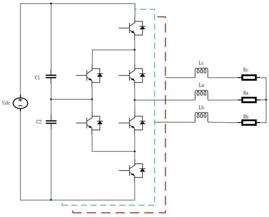
Figure 1.
ANPC converter circuit topology.
During the operation of the inverter, the IGBTs and diodes switch between dynamic and static states, resulting in losses mainly in switching and conduction. In the traditional NPC three-level inverter topology, the junction temperature imbalance problem caused by the loss imbalance on the power switching devices limits the development of this topology, and the device that bears the most losses limits the switching frequency and output power of the whole inverter. The ANPC three-level inverter solves the problem by replacing the clamping diode in the NPC three-level inverter with an inverse-parallel continuity diode power switching device and adding a redundant zero-state output method and provides more selectable switching states to equalize the loss distribution. However, here we only model the ANPC and do not discuss much about the device losses of the inverter.
This three-level converter architecture consists of six fully controlled power devices, Sx1 through Sx6, and two dc bus capacitors, C1 and C2. Udc represents the dc bus voltage; ic1 and ic2 denote the currents of the two dc bus capacitors; Ua, Ub, and Uc are the corresponding phase voltages; ia, ib, and ic denote the corresponding phase currents; and RL is the load resistance. For the commutation analysis of the three-level ANPC converter, the switching states are listed in Table 1. Current flow through the load terminal is considered positive, and the reverse is considered the negative direction of the circuit. In the following cases:

Table 1.
Switching state of phase X of the three-level ANPC main circuit topology.
- When the current is positive, the output state switches bi-directionally between P and O. There are two current-switching paths: bi-directional switching between P and OV1 and bi-directional switching between P and OV2, which corresponds to Figure 2a,b.
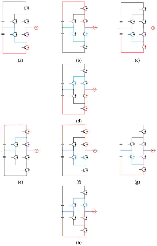 Figure 2. ANPC converter switched-current modes. (a) Positive current state P and OV1, (b) Positive current state P and OV2, (c) Positive current state N and ow1, (d) Positive current state N and OV2, (e) Negative current state P and OV1, (f) Negative current state P and OW2, (g) Negative current state N and OW1, (h) Negative current state N and OV2.
 - When the current is positive, the output state switches bi-directionally between N and O. There are two current-switching paths: bi-directional switching between N and OW1 and bi-directional switching between N and OV2, which corresponds to Figure 2c,d.
- When the current is negative, the output state switches bi-directionally between P and O. There are two current-switching paths: bi-directional switching between P and OV1 and bi-directional switching between P and OW2, which corresponds to Figure 2e,f.
- When the current is negative, the output state switches bi-directionally between N and O. There are two current-switching paths: bi-directional switching between N and OW1 and bi-directional switching between N and OV2, which corresponds to Figure 2g,h.
2.2. Discrete Mathematical Modeling of ANPC
The discrete mathematical model is the basis for the study of the three-level converter. The load of the three-level converter is a resistive inductive star-shaped load based on the Kirchhoff’s voltage principle to establish the dynamic expression of the load as:
where R is the load resistance, L is the load inductance, U (t) is the value of the voltage transformed with time at the output of each phase of the load, and i (t) is the value of the current transformed with time at the output of each phase of the load. When the sampling period is relatively small, in order to be able to simplify and analyze the working principle of the system, this chapter uses the formula shown below to simulate the derivatives.
where x(k), x (k 1) are the measured values at time k and time k 1, respectively. The condition holds only if the sampling period Ts is relatively small. and represent the instantaneous values of the load current at moments k and k + 1, respectively. The discrete model of the dynamic load current of the converter can be obtained by bringing this equation into the above equation, as shown below:
2.3. IGBT Switching Control
If a conventional FCS-MPC controls an ANPC three-level inverter, the normal thinking is as follows:
- Using an ANPC discrete time model of three-level inverter to predict the change in load current, midpoint potential, etc. at the next future moment.
- The desired parameters are controlled using cost functions and weight factors.
- The inverter is controlled by selecting one of the 27 switching states that minimizes the cost function.
However, this control method needs to sample and calculate the currents of 27 switching states in each sampling cycle to calculate the optimal reference voltage, which is a large amount of computation. Based on the consideration of optimizing the FPGA resources and reducing the time step, this paper proposes a method to take the half-bridge unit as a single computation unit and to take the input current of a single phase in the three phases, as well as the DC bus voltage as a judgment condition, to establish a half-bridge unit with three switching transients corresponding to three voltage levels of each output voltage. Switching transients correspond to the three voltage levels of the output voltage of each phase. Three three-step FCS-MPC-controlled half-bridge units are used in parallel instead of the conventional serial operation of traversing 27 output states, which optimizes the time step and enables stable control of the circuit.
The control steps are shown in the Figure 3. The main control for the following three steps:
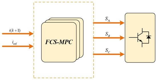
Figure 3.
Improved FCS-MPC control strategy.
- Define the reference current iref; set the input voltage and input current.
- Predict the next moment of i(k) based on switching states and measurements.
- Calculate the cost function using the predicted values, select the predicted values, and switch the output state.
Among them, the commonly used form of the cost function mainly includes the absolute value of the error or the quadratic value of the error, and the cost function is shown in Equation.
As shown in Figure 4, by comparing the current waveforms generated by the ANPC with FCS-MPC control and the ANPC with SPWM control, we observe that they show consistent basic patterns and the same trend. This indicates that the generated waveforms are accurate and reliable in general. However, it is worth noting that the waveforms generated by the FCS-MPC control show significant advantages in terms of smoothness and volatility, with less fluctuation and higher smoothness compared to the SPWM control. By simulating and comparing the two methods, we can clearly observe that the FCS-MPC algorithm has significant advantages in terms of output current and other aspects.
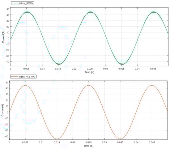
Figure 4.
Current waveform comparison.
3. Circuit Modeling and Analysis
3.1. Circuit Dividing
In power electronic circuit modeling, correctly dividing the whole circuit into several independent subsystems is a crucial step in order to implement efficient parallel computation. When all the subsystems can be fully decoupled and processed in parallel, the overall computational efficiency can be greatly improved. This is because, compared to traditional serial processing, the decoupled subsystems can run independently of each other without waiting for the result of the previous level of operation, avoiding the computational delay caused by the one-shot delay. This not only reduces the matrix dimension and computational effort, but also improves the computational efficiency by adopting a parallel operation mode between the switch-containing nonlinear system and other subsystems (which are usually linear).
The Figure 5 shows the operation of each subsystem after decoupling. From the figure, it can be seen that the size of each subsystem in parallel processing represents the respective amount of computation and reflects the computation time consumed by the length of the arrows. If all the subsystems are processed sequentially one by one, the total time required for the whole model is the sum of the computation time of each subsystem; however, after parallel processing, all the computations can be completed by spending only the time taken by the slowest subsystem, which greatly reduces the total time consumed. In this case, the speed of the entire model run is limited only by the amount of computation of the largest subsystem.
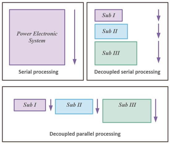
Figure 5.
Comparison of decoupling approaches.
By the above method, ANPC is divided into three independent subsystems, as shown in the Figure 6 and Figure 7. ANPC is a typical three-phase symmetrical power electronic system that is divided into subsystems I, II, and III at the DC bus capacitance and three-phase shunt inductance. And, by symmetry, subsystem II can be divided into three sub-circuits, X. II (X = A, B, C). For three-phase symmetrical circuits, since the three inductors are connected in parallel between the two subsystems, it is no longer a general one-port network, and it is necessary to specialize the three-phase inductors in order to achieve no delay. At this point, we can choose two ways to deal with the three-phase inductors.
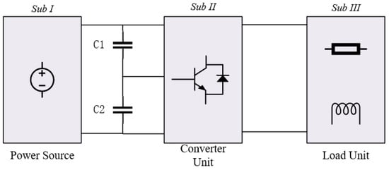
Figure 6.
Original ANPC converter circuit.
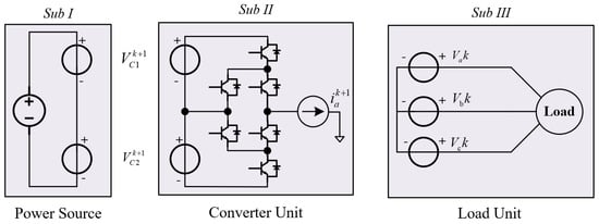
Figure 7.
Equivalent circuit of ANPC converter.
- Turning a three-phase inductor equivalent current source into two one-port circuits.
- Assuming the presence of a load-side neutral point n, the inductive current per phase can be calculated for the three-phase circuit of subsystem II in accordance with Kirchhoff’s laws of voltage and current, provided that the neutral voltages between the subsystems are compensated for.
In this paper, the second method is used for processing.
3.2. Discretized Parallel Solution Method
In most cases, a power electronic system can be represented as a state space equation having an initial value . Discretization of the original continuous system and numerical analysis methods are utilized as an approximation of the solution shown in the equation. The most common method is the explicit Euler method, which approximates the derivatives in ordinary differential equations by the mean deviation
obtained directly. If the initial value is known, then can be calculated one by one, n = 1,2,3…
An approximation with the right rectangular formula in Equation yields another formula
However, the right side of the formula contains the unknown , which is actually a functional equation about . It is commonly solved by an iterative method, and the iterative process is essentially a gradual explicitization. Until hL < 1, the iterative method converges to the solution .
Another method with higher accuracy than the implicit Euler method is realized by approximating the right side of the equation with a trapezoidal product formula. The essence of this is similar to the implicit Euler method, which is an implicit single-step method solved by an iterative method.
It is well-known that the implicit method approach is more stable and accurate. However, its algorithm is complex, and when using the iterative formula for practical calculations, the value of the function has to be recalculated for each iteration. The iteration has to be repeated several times, which is a large and often-unpredictable amount of calculations, and the unknown number of iterations may lead to an overrun in the real-time simulation process. In order to control the amount of computation, the algorithm is usually simplified by iterating only once or twice before moving on to the next step in the computation. The prediction correction system thus created is also called an improved Eulerian formulation.
Predictor Step:
Corrector Step:
From the Figure 8, it is clear that the corrector step uses the value depending on the computational result of the predictor step, while the global computational time step h is the sum of the computational time of the two steps.
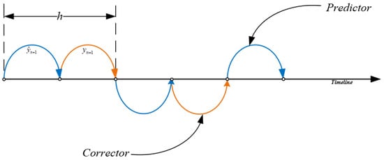
Figure 8.
Steps for the prediction correction system.
The computation time can be reduced by a factor of two if we can compute the predictor and the corrector variables at the same time. If the predictor step can be delayed by one time step, the results of the predictor step can be directly obtained by the corrector at the current moment. As shown in the Figure 9. This method can be used effectively when the simulation time step is relatively small, which is the case for real-time power electronic simulation modeling.
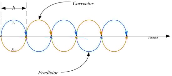
Figure 9.
Steps for the improved predictor–corrector system.
Predictor Step:
Corrector Step:
Lipschitz continuity theory is a mathematical concept used to describe the variability of a function, which defines the range of slope changes of a function at a given point. In this way, we can determine whether a solver is stable or not in the case where Re(K) < 0. In this case, if a function satisfies Lipschitz continuity, it has a finite range of slope change, which means that when we change the input values during the solving process, the output values will not change too much. Furthermore, by applying the improved solution equation to the test equation dy/dt = Ky, we can further deduce that this method is also numerically stable. Therefore, we can say that this solver is stable.
4. Experiment
4.1. Experimental Environment
The experiments were carried out on the official Speedgoat real-time simulator from Math (Speedgoat, Bern, Switzerland), and the SN codes for the two Speedgoat devices are 8530 and 8767. We used a model IO324 simulator, with an Intel Core i7 4. 2 GHz 4-core CPU, supporting multiple I/O interfaces and a Xilinx Artix-7 FPGA board.
The Speedgoat real-time simulator is based on Math Works Simulink Real-Time Toolbox, which can realize seamless connection with MATLAB/Simulink (version 2022b). By building the Simulink model on the host computer, it can realize data flow and communication, support one-key compilation, and download to the Speedgoat real-time simulator. The Speedgoat real-time simulator supports real-time online adjustment of parameters and real-time viewing of signals, which provides the basis for real-time display and modification of data in the equivalent model simulation. The interface functions of the FPGA modules provided by Speedgoat are configurable, highly flexible, and can be programmed using HDL Coder in a Matlab environment and all digital and analog I/O channels can be accessed in Workflow Advisor. When the I/O port functions are special, such as PWM, SPI, I2C, Encoder, etc., they can be programmed to be realized with the FPGA’s I/O channels, and the bitstream files provided by Speedgoat can be reconfigured with FPGA board functions. The rapidly configurable FPGAIO module provides a flexible real-time test environment and the ability to iterate designs more quickly.
The overall simulation design as the follows Figure 10: two Speedgoat real-time simulators are used for real-time simulation, one of which runs the FCS-MPC control algorithm as a controller and runs in its CPU environment, the other of which runs the simulation circuit as a controlled object, in which the real-time simulator interacts with the upper computer through Ethernet communication. During real-time operation, the collected current and voltage information collected by the controlled circuit is transmitted in real time via analog signals, while the controller performs control calculations in real time after receiving the voltage and current signals and sends the results to the controlled circuit in real time via digital signals.
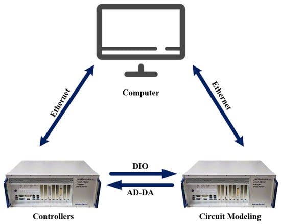
Figure 10.
Overall simulation design framework.
The specific environment for the experiment is shown in the following Figure 11. (1) is the mainframe, (2) is an oscilloscope that allows real-time observation of the output waveforms, (3) is the Speedgoat (1) simulator, which performs real-time simulation of the circuit, and (4) is the Speedgoat (2) simulator, which is the controller that runs the model in the internal FPGA control algorithms in the CPU environment and through the analog and digital of the (5) and (6) boards.
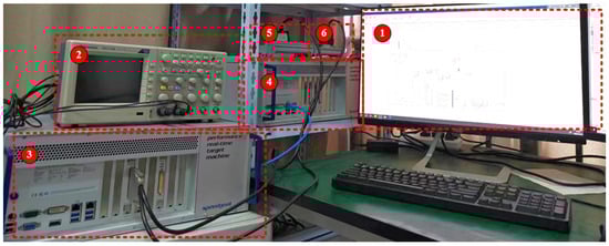
Figure 11.
Experimental environment.
4.2. Real-Time Simulation Results
In this section, we delve into and compare the real-time results of the hardware-in-the-loop simulation. The design of this experiment includes a comparison between parallel decoupling and serial decoupling, as well as a performance comparison with SPS. In order to verify the accuracy of the modeling, we first simulated the model on the FPGA board using the parallel decoupling and serial decoupling methods, both of which use the same simulation parameters as the SPS, as shown in Table 2.
Table 2.
Variable values.
As shown in the Figure 12 , we performed a detailed comparison experiment on the output current . Throughout the simulation moments, we noticed a 2.7 percent error at moment 0.002 s. Although this small magnitude of error is observable at one moment, at other moments, we observed cases where the simulation performed well, showing good accuracy.
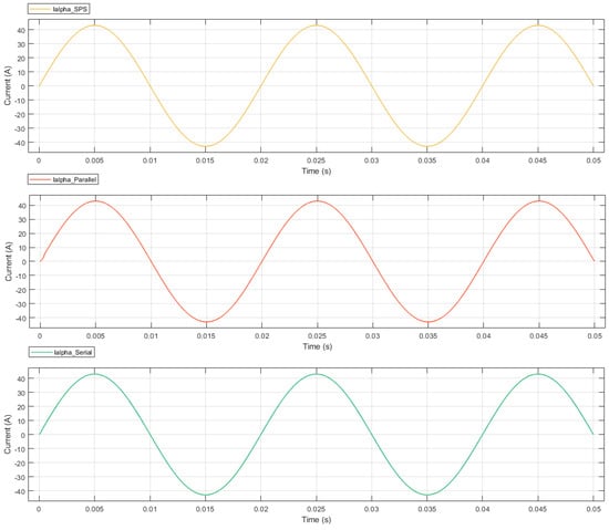
Figure 12.
Comparison of output current.
The values in the Figure 13 and Figure 14 show that parallel decoupling has a smaller deviation in the results subtracted from SPS compared to serial decoupling. This shows that it is not the case that the computational speed is increased at the expense of the computational accuracy, but on the contrary, the experimental results show that the parallel decoupling has a better accuracy.
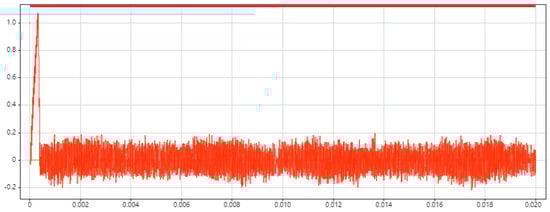
Figure 13.
Error between parallel decoupling and SPS.
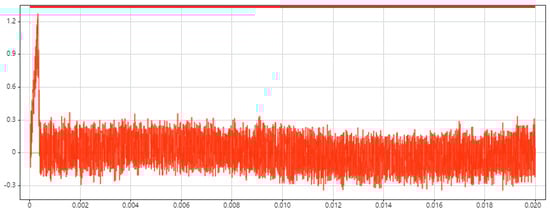
Figure 14.
Error between serial decoupling and SPS.
We paid special attention to the experiments under three-phase load unbalance conditions, in which we doubled the load inductance of one phase to verify the performance of our mathematical model under such real-world conditions. As shown in the Figure 15, the experimental results show that our mathematical model still performs well under three-phase unbalanced load conditions. Despite the different load conditions, the system is still able to accurately simulate the behavior of the ANPC system, and the simulation results are consistent with the theoretical expectations.
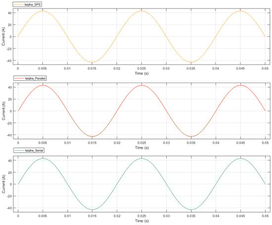
Figure 15.
Output current under three-phase unbalanced conditions.
4.3. Resource Consumption and Time Step
As shown in the Table 3, parallel decoupling requires more registers for parallel operations, while serial decoupling requires more adders for computations. Since real-time simulation is not performed for a complex system, the resource usage comparison is not obvious enough, but the gap can still be seen.
Table 3.
Resource consumption and time step.
In general, the minimum delay path determines the minimum number of simulation steps that the system can perform. In this regard, the minimum number of simulation steps that can be performed by a parallel decoupled operation system requires 58 ns. In contrast, serial decoupling requires 83 ns, so it is evident that parallel decoupling has a significant advantage in terms of real-time simulation step size.
Overall, by using parallel decoupling, the system achieves a significant improvement in the real-time simulation step size. The actual running results show that the no-delay decoupling requires only 58 ns of step length, while the serial decoupling requires 83 ns. This clearly shows that the parallel decoupling can shorten the real-time simulation step length more effectively and improve the real-time performance of the system.
5. Conclusions
To summarize the above research, this paper presents an effective modeling and simulation methodology through an in-depth study of multi-switching power electronic circuits with complex variable topologies, especially three-level active neutral point clamped (ANPC) converters. Facing the challenges of expanding circuit scale and increasing real-time simulation resource consumption, we adopt the strategy of parallel computation after subsystem partitioning, which successfully solves the problems of simulation delay and numerical oscillations, thus improving the numerical stability of the modeling and real-time simulation efficiency.
For the mathematical model solution, we introduce a modified prediction correction method to provide higher accuracy and higher stability, avoiding the low accuracy and significant errors that may result from the traditional forward Eulerian method. In addition, the improved FCS-MPC strategy is used to control the switching transients of the ANPC model, which successfully achieves a superior control effect.
Finally, the empirical results on the Speedgoat testbed show that our method successfully achieves a simulation step size lower than 60 ns, verifying the practicality and effectiveness of the proposed method. By comparing the simulation results with those of the Matlab Simpower system, we are able to objectively assess the accuracy of the constructed model.
In summary, this study not only proposes innovative solutions in the field of power electronic circuit modeling and simulation, but also provides a useful reference for future research on similar complex systems. These results are of great significance for improving the performance, stability, and real-time simulation efficiency of power electronic systems and contribute valuable research results to the development of the power electronics field.
Author Contributions
Conceptualization, X.G., Y.H. and S.L.; Methodology, X.G., Y.H. and S.L.; Software, C.L.; Validation, C.L.; Writing—original draft, C.L.; Writing—review and editing, S.L. and Z.S.; Supervision, Z.S.; Project administration, Z.S.; Funding acquisition, Z.S. All authors have read and agreed to the published version of the manuscript.
Funding
This research was funded by the Nuclear Power Operations Research Institute (NPRI) under the project Voltage Transformer Online Monitoring and Fault Diagnosis Project Development Technology, Licence No. JYJFY-22006900-000. Furthermore, this research was partially supported by the Xiamen Key Laboratory of Frontier Electric Power Equipment and Intelligent Control.
Data Availability Statement
Data are contained within the article.
Conflicts of Interest
Authors Xin Gao and Yuanyuan Huang were employed by the company Nuclear Power Operations Research Institute (NPRI). The remaining authors declare that the research was conducted in the absence of any commercial or financial relationships that could be construed as a potential conflict of interest.
References
- Bruckner, T.; Bemet, S. Loss balancing in three-level voltage source inverters applying active NPC switches. In Proceedings of the 2001 IEEE 32nd Annual Power Electronics Specialists Conference (IEEE Cat. No.01CH37230), Vancouver, BC, Canada, 17–21 June 2001; Volume 2, pp. 1135–1140. [Google Scholar]
- Bruckner, T.; Bernet, S.; Guldner, H. The active NPC converter and its loss-balancing control. IEEE Trans. Ind. Electron. 2005, 52, 855–868. [Google Scholar] [CrossRef]
- Sun, Z.; Ma, G.; Xu, S.; Zhang, H.; Ren, G. Reduced Vector Model Predictive Control of ANPC Inverter for PMSM Drives with Optimized Commutation. IEEE Trans. Transp. Electrif. 2022, 8, 3177–3191. [Google Scholar] [CrossRef]
- Vijeh, M.; Rezanejad, M.; Samadaei, E.; Bertilsson, K. A General Review of Multilevel Inverters Based on Main Submodules: Structural Point of View. IEEE Trans. Power Electron. 2019, 34, 9479–9502. [Google Scholar] [CrossRef]
- Feng, Z.; Zhang, X.; Wang, J.; Yu, S. A high-efficiency three-level ANPC inverter based on hybrid SiC and Si devices. Energies 2020, 13, 1159. [Google Scholar] [CrossRef]
- Dong, L.; Zang, Z.; Ming, Y.; Zhao, R.; Ma, W.; Hu, H. Research on the Coordination Suppression Strategy of Neutral Point Potential and Common Mode Voltage for NPC Three-Level Inverter. Symmetry 2023, 15, 35. [Google Scholar] [CrossRef]
- Zhang, Y.; Hu, C.; Wang, Q.; Zhou, Y.; Sun, Y. Neutral-point potential balancing control strategy for three-level ANPC converter using SHEPWM scheme. Energies 2019, 12, 4328. [Google Scholar] [CrossRef]
- Xu, X.; Liu, N.; Wang, K.; Zheng, Z.; Li, Y. Modulation and control of an ANPC/H-bridge hybrid inverter for ship electric propulsion drives. In Proceedings of the 2019 IEEE 22nd International Conference on Electrical Machines and Systems (ICEMS), Harbin, China, 11–14 August 2019; pp. 1–5. [Google Scholar]
- Jing, X.; He, J.; Demerdash, N.A. Application and losses analysis of ANPC converters in doubly-fed induction generator wind energy conversion system. In Proceedings of the 2013 IEEE International Electric Machines & Drives Conference, Chicago, IL, USA, 12–15 May 2013; pp. 131–138. [Google Scholar]
- Zhang, D.; He, J.; Pan, D. A megawatt-scale medium-voltage high-efficiency high power density “SiC+ Si” hybrid three-level ANPC inverter for aircraft hybrid-electric propulsion systems. IEEE Trans. Ind. Appl. 2019, 55, 5971–5980. [Google Scholar] [CrossRef]
- Radomsky, L.; Mallwitz, R. Review, Comprehensive Analysis and Derivation of Analytical Power Loss Calculation Equations for Two-to Three-Level Midpoint Clamped Inverter Topologies with Hybrid Switch Configurations. Energies 2023, 16, 6710. [Google Scholar] [CrossRef]
- Lee, J.S.; Choi, G. Modeling and hardware-in-the-loop system realization of electric machine drives—A review. CES Trans. Electr. Mach. Syst. 2021, 5, 194–201. [Google Scholar] [CrossRef]
- Sorto-Ventura, K.R.; Li, W.; Al-Haddad, K. An equivalent model of the paralleled modular ANPC converter with a decoupled DC link for real-time simulation. In Proceedings of the IECON 2021—47th Annual Conference of the IEEE Industrial Electronics Society, Toronto, ON, Canada, 13–16 October 2021; pp. 1–6. [Google Scholar]
- Missula, J.V.; Adda, R.; Tripathy, P. Averaged modeling and SRF-based closed-loop control of single-phase ANPC inverter. IEEE Trans. Power Electron. 2021, 36, 13839–13854. [Google Scholar] [CrossRef]
- Zolfaghar, M.; Najafi, E.; Hasanzadeh, S. A modified diode clamped inverter with reduced number of switches. In Proceedings of the 2018 9th Annual Power Electronics, Drives Systems and Technologies Conference (PEDSTC), Tehran, Iran, 14–15 February 2018; pp. 53–58. [Google Scholar]
- Dai, X.; Ke, C.; Quan, Q.; Cai, K.Y. Simulation credibility assessment methodology with FPGA-based hardware-in-the-loop platform. IEEE Trans. Ind. Electron. 2020, 68, 3282–3291. [Google Scholar] [CrossRef]
- Li, Z.; Xu, J.; Wang, K.; Li, G.; Wu, P.; Zhang, L. An FPGA-Based Hierarchical Parallel Real-Time Simulation Method for Cascaded Solid-State Transformer. IEEE Trans. Ind. Electron. 2022, 70, 3847–3856. [Google Scholar] [CrossRef]
- Bai, H.; Luo, H.; Liu, C.; Paire, D.; Gao, F. A device-level transient modeling approach for the FPGA-based real-time simulation of power converters. IEEE Trans. Power Electron. 2019, 35, 1282–1292. [Google Scholar] [CrossRef]
- Li, Q.; Bai, H.; Breaz, E.; Roche, R.; Gao, F. ANN-Aided Data-Driven IGBT Switching Transient Modeling Approach for FPGA-Based Real-Time Simulation of Power Converters. IEEE Trans. Transp. Electrif. 2022, 9, 1166–1177. [Google Scholar] [CrossRef]
- Milton, M.; Benigni, A. Latency insertion method based real-time simulation of power electronic systems. IEEE Trans. Power Electron. 2017, 33, 7166–7177. [Google Scholar] [CrossRef]
- Liu, C.; Ma, R.; Bai, H.; Gechter, F.; Gao, F. A new approach for FPGA-based real-time simulation of power electronic system with no simulation latency in subsystem partitioning. Int. J. Electr. Power Energy Syst. 2018, 99, 650–658. [Google Scholar] [CrossRef]
Disclaimer/Publisher’s Note: The statements, opinions and data contained in all publications are solely those of the individual author(s) and contributor(s) and not of MDPI and/or the editor(s). MDPI and/or the editor(s) disclaim responsibility for any injury to people or property resulting from any ideas, methods, instructions or products referred to in the content. |
© 2025 by the authors. Licensee MDPI, Basel, Switzerland. This article is an open access article distributed under the terms and conditions of the Creative Commons Attribution (CC BY) license (https://creativecommons.org/licenses/by/4.0/).