Abstract
Printed circuit board (PCB) defect detection is essential for ensuring manufacturing quality and product reliability in electronics production. PCB designs often exhibit inherent symmetry in circuit layouts and periodic patterns, which defects disrupt by introducing asymmetries detectable in spatial and frequency domains. Contemporary methods predominantly emphasize either global context modeling or local detail preservation, yet fail to synergistically leverage their complementary characteristics. Existing approaches predominantly constrain operations to the spatial domain, neglecting complementary frequency-domain representations that encode periodic structures and spectral anomalies. We present PCB-FS, a unified frequency–spatial learning framework that augments YOLOv8 with three synergistic components: (i) Dual-Domain Convolution (DD-Conv) for adaptive spatial frequency feature extraction, (ii) Global–Local Axial Attention (GLA-Attention) for context-aware defect modeling, and (iii) Cross-Stage Partial Dynamic Shifted Large Kernel Convolution (C2f-DSLKConv) for efficient large-receptive-field fusion. Our DD-Conv module adaptively fuses spatial and frequency-domain representations, while the GLA-Attention mechanism enhances global context modeling without sacrificing local detail preservation. The C2f-DSLKConv module further enables efficient large-receptive-field spatial modeling and hierarchical feature aggregation. Our method exploits symmetry-breaking artifacts in PCB layouts to detect structural anomalies, achieving superior defect localization accuracy. A comprehensive evaluation on the enhanced PCB surface defect dataset (DsPCBSD+) demonstrates that PCB-FS achieves 86.2% mAP@50 and 52.4% mAP@50-95, establishing new state-of-the-art performance with significant margins over existing methods. Integrating frequency and spatial domain features significantly enhances PCB defect detection reliability and efficiency in practical applications.
1. Introduction
Printed circuit board (PCB) designs inherently leverage symmetry—mirrored traces and periodic layouts—to ensure electrical balance and manufacturing efficiency. Defects disrupt inherent symmetries, yielding measurable asymmetries in spatial structures and frequency spectra. PCB defect detection [,,,] is essential for modern electronics manufacturing, directly impacting product reliability, safety, and cost-effectiveness [,]. As component miniaturization and circuit density increase, detecting subtle defects—including micro-cracks, solder bridges, and foreign object contamination—becomes increasingly challenging and critical [,]. Escalating PCB complexity necessitates robust defect detection to ensure product quality and prevent costly failures, driving advanced detection method development [,]. Multi-domain feature integration emerges as a critical performance driver [].
Existing PCB defect detection methods dichotomize into global and local feature-based approaches. Global methods leveraging transformer architectures or global attention mechanisms effectively capture holistic structural patterns and long-range dependencies [,,]. Local methods emphasize fine-grained defect characterization through convolutional neural networks and localized attention mechanisms [,,]. Notable approaches include DSASPP [], which aggregates multi-scale contextual features via dilated convolutions, and C2fCBAM [], integrating channel-wise and spatial attention mechanisms for enhanced local feature representation. Prior approaches independently process global and local features, underutilizing their complementary characteristics. This decoupling yields suboptimal detection performance for small-scale or irregular defects within complex backgrounds [,].
Conventional PCB defect detection predominantly operates in the spatial domain, leveraging pixel-level representations with either handcrafted or learned spatial features [,,]. Despite achieving significant performance gains, existing methods exhibit limited efficacy in detecting subtle or ambiguous defects lacking salient spatial-domain characteristics [,]. Existing methods predominantly neglect the frequency domain, which captures periodic structures and spectral anomalies inherent to PCB layouts. Recent studies demonstrate that frequency-domain analysis, including Fourier and Fractional Fourier Transforms, effectively captures defect-induced perturbations in regular frequency patterns, thereby providing a powerful complementary perspective for defect detection [,,]. However, existing frequency-domain methods exhibit limited adaptability to PCB-specific patterns and rarely integrate with spatial-domain learning within unified frameworks [,].
Recent advances demonstrate that large-kernel convolutions enhance defect detection by capturing long-range spatial dependencies and structural patterns [,,,,]. PCBA-YOLO [] incorporates large-kernel convolutions into the YOLOv5 backbone, expanding the effective receptive field to enhance printed circuit board assembly (PCBA) defect detection accuracy. Similarly, YOLO-RLC [] augments YOLOv5 with a residual large-kernel backbone that captures global context, yielding substantial accuracy gains for PCB defect detection. Recent works advance image enhancement through frequency-aware representations (FAIR []), spatial frequency fusion via atrous spatial pyramid pooling (DSASPP []), and deformable convolution-dense pyramid integration for surface defect detection []. While existing multi-scale approaches advance feature representation, they exhibit critical limitations in adaptive frequency learning and efficient large-kernel fusion. PCB-FS overcomes these constraints through integrated modules, enabling robust PCB defect detection. Standard large-kernel convolutions incur prohibitive computational overhead and parameter explosion, rendering them infeasible for real-time and resource-constrained deployments.
To address these limitations, we propose PCB-FS, a frequency–spatial feature learning framework for PCB defect detection. Built upon an enhanced YOLOv8 architecture, PCB-FS integrates three key components: (1) a learnable Dual-Domain Convolution (DD-Conv) module, (2) a Global–Local Axial Attention (GLA-Attention) mechanism, and (3) a Cross-Stage Partial with Dynamic Shifted Large Kernel Convolution (C2f-DSLKConv) module that replaces the standard Darknet block in C2f structures with dynamic shifted large kernel convolution for efficient spatial modeling and feature fusion. The DD-Conv module adaptively fuses spatial and frequency-domain features, enabling defect-specific spectral signature detection and structural anomaly localization []. The GLA-Attention block augments global context modeling while preserving local spatial details, enabling robust multi-scale defect detection in complex scenarios [,,]. The C2f-DSLKConv module achieves efficient large receptive field spatial modeling via dilated separable long-range kernel convolutions, enabling the network to capture global dependencies and complex defect patterns while reducing computational complexity. These modules achieve robust PCB defect detection through complementary spatial–frequency-domain fusion.
YOLOv8 was selected as the base architecture due to its superior balance of real-time inference speed (up to 110 FPS on our hardware), modular design for easy customization, and state-of-the-art accuracy in object detection benchmarks, outperforming earlier versions like YOLOv5 in efficiency and flexibility while being more stable than emerging variants like YOLOv10 or YOLOv11 at the time of this research.
Standard YOLOv8, while effective for general object detection, has limitations in PCB defect scenarios: it relies solely on spatial features, struggles with Global–Local context balancing for multi-scale defects, and incurs high costs for large receptive fields. Our modifications address these: DD-Conv integrates adaptive frequency-domain processing to capture spectral anomalies; GLA-Attention enhances global modeling while preserving local details; and C2f-DSLKConv provides efficient large-kernel fusion for long-range dependencies.
The main contributions of this paper are summarized as follows:
- We introduce Dual-Domain Convolution (DD-Conv), a frequency-adaptive filtering module that simultaneously captures spatial anomalies and defect-specific spectral signatures in PCB imagery.
- We propose a Global–Local Axial Attention (GLA-Attention) module that jointly captures global context and preserves fine-grained local details, yielding substantial improvements in multi-scale and complex defect detection.
- We present the Cross-Stage Partial with Dynamic Shifted Large Kernel Convolution (C2f-DSLKConv) module, which substitutes the conventional Darknet block within the C2f architecture via dynamic shifted large kernel convolution, thereby enabling efficient large receptive field spatial modeling and feature fusion.
- We present PCB-FS, a YOLOv8-based architecture that integrates DD-Conv and GLA-Attention modules, achieving state-of-the-art performance on the DsPCBSD+ dataset with real-time inference suitable for industrial deployment.
The rest of this paper is organized as follows: Section 2 discusses related work in PCB defect detection, including traditional methods, deep learning approaches, attention mechanisms, and frequency-domain deep learning approaches. Section 3 provides the proposed methodology, detailing the PCB-FS framework, Dual-Domain Convolution module, Global–Local Axial Attention mechanism, and Cross-Stage Partial with Dynamic Shifted Large Kernel Convolution module. Section 4 presents the experiment and analysis, including dataset description, implementation details, evaluation metrics, experimental results, and ablation studies, demonstrating the effectiveness of each component. Section 5 concludes the paper with a summary of contributions and future work directions.
2. Related Work
Our work encompasses four key areas: traditional approaches, deep learning methodologies, transformer architectures, and attention mechanisms.
2.1. Traditional Methods
PCB defect detection has evolved through three distinct paradigms, each addressing predecessor limitations while introducing new challenges. First approaches relied on basic image processing techniques like template matching. The NCC-based method [] established baselines through neighborhood window correlation but suffered from rigid template dependencies and sensitivity to positional shifts. These systems required precise alignment and struggled with defect variability, motivating the development of more adaptive techniques. Second methods incorporated machine learning with handcrafted features. Gabor-wavelet hybrids [] improved noise robustness through 1D descriptor conversion, while solder paste analysis [] employed color biometric features. However, manual feature engineering limited their ability to capture subtle defect patterns, and performance degraded with unseen PCB layouts. This feature engineering bottleneck drove the need for probabilistic approaches. Third hybrid systems combined probabilistic modeling with traditional vision. Gaussian mixture models [] addressed complex backgrounds through Markov random fields, and Fourier descriptors [] enabled rotation-invariant recognition. Yet these methods required extensive parameter tuning and struggled with real-time implementation due to computational complexity.
As identified in comprehensive surveys [], three fundamental limitations persist across all generations: (1) manual threshold sensitivity, (2) limited cross-domain generalization, and (3) scaling challenges with high-density PCBs. These unresolved issues create critical demand for data-driven approaches that automatically learn defect representations while maintaining computational efficiency.
2.2. Deep Learning Approaches
Building upon the limitations of traditional methods in handling complex defect patterns and real-time requirements, deep learning approaches have emerged as the dominant paradigm through two fundamental architectural innovations:
2.2.1. Two-Stage Detectors
Two-stage object detectors, such as the R-CNN series, follow a pipeline of region proposal, feature extraction, and classification/regression [,,,,]. Improvements like Fast R-CNN and Faster R-CNN have enhanced efficiency by integrating region proposal and feature extraction, while Cascade R-CNN and Sparse R-CNN further refine detection quality and speed. In PCB defect detection, these models are often adapted to better capture microscopic defect patterns, for example, through dual-branch U-Net architectures [] or deformable transformers []. Two-stage detectors suffer from inherent computational redundancy due to their separate region proposal and detection mechanisms, resulting in low inference speeds (<20 FPS) that fail to meet real-time industrial inspection requirements. Furthermore, their multi-stage cascade design creates suboptimal end-to-end optimization, particularly degrading detection accuracy for small soldering defects in PCBs.
2.2.2. One-Stage Detectors
The aforementioned limitations (high latency and low efficiency) have motivated the development of one-stage detectors. The YOLO series addresses these issues by formulating object detection as a unified regression problem, directly predicting bounding boxes and class probabilities while eliminating the need for region proposal stages. This approach maintains comparable detection accuracy while achieving over 10× speed acceleration in inference, making it particularly suitable for real-time industrial quality inspection scenarios. The CFR-enhanced YOLOv5s [] introduces coordinate feature refinement modules with spatial-channel attention gates to resolve multi-level feature conflicts. FPGA-accelerated YOLOx-Plus [] implements hardware-aware optimizations through layer fusion and 8-bit quantization kernels. Edge deployment variants like EEDD [] propose edge-guided energy maps for micro-defect detection while reducing model complexity.
Current research focuses on two technical dimensions. Multi-scale Processing: The DSASPP module [] proposes a depthwise separable atrous spatial pyramid pooling structure that combines dilated convolutions (rates = 6, 12, 18) with global context aggregation through parallel pyramid branches. This architecture addresses the challenge of detecting sub-millimeter defects by capturing multi-scale contextual information while maintaining computational efficiency. Attention Mechanisms: C2fCBAM [] introduces a dual-attention mechanism that embeds concurrent channel-spatial attention blocks within the C2f backbone structure. The design solves attention dilution in multi-defect scenarios through learnable spatial offset modulation, achieving an 18.7% reduction in false positives for high-density PCB regions compared to baseline CBAM implementations.
2.3. Attention Mechanisms
Attention mechanisms have been widely integrated into convolutional networks to enhance feature representation by focusing on important regions or channels [,,]. Early approaches like SENet [] and ECA-Net [] recalibrate channel-wise responses, while CBAM [] and Coordinate Attention [] combine channel and spatial attention to improve object detection and mobile network performance. More advanced designs, such as Non-local Networks [] and Vision Transformer (ViT) [], model long-range dependencies through self-attention, and Swin Transformer [] enables multi-scale feature learning for dense prediction tasks. Recent works have further explored multi-scale attention, integrating pyramid self-attention and dilated convolutions to capture cross-scale dependencies [,,]. These mechanisms have improved accuracy in various vision tasks, including PCB defect detection. However, as attention modules become more complex, they often introduce significant computational overhead and may dilute critical local features, especially in high-density or small-defect scenarios []. This highlights the need for lightweight, effective attention designs that can balance global context and local detail, forming a key motivation for our research.
Transformer architectures have shown strong potential in visual tasks due to their global attention mechanisms [,]. Models like Swin-Transformer [] and PPLA-Transformer [] have been adapted for PCB defect detection, achieving high accuracy by capturing long-range dependencies and multi-scale features. To reduce the high computational cost of standard transformers, methods such as pyramid pooling [], linear attention [], and cross-scale feature pyramids [] have been proposed. Notably, balancing local features and global context emerged as a critical challenge. PPLA-Transformer [] proposes a pyramid-pooled linear attention mechanism integrated with partial convolution enhancement and dynamic cross-stage feature fusion, innovatively addressing the computational inefficiency of traditional Transformers while resolving local feature degradation in linear attention and multi-scale semantic integration challenges for industrial defect detection. DefT [] hybridized convolutional and attention mechanisms, yet its hybrid architecture increased parameters by 40%. Wang et al.’s Defect Transformer (DefT) [] integrated positional awareness with lightweight attention, achieving a 94.3% mAP on steel plate defects, but slowed to 28 FPS on high-resolution PCB images, exposing limited industrial adaptability.
2.4. Frequency-Domain Deep Learning Approaches
Recent years have witnessed a growing interest in integrating frequency-domain analysis with deep learning for visual inspection tasks, including PCB defect detection. Unlike traditional spatial-domain methods, frequency-domain approaches leverage spectral representations to capture periodic structures, texture regularities, and subtle anomalies that may be less discernible in the spatial domain [,]. Early works typically applied standard Fourier transforms as a preprocessing step or as an auxiliary feature extractor, but these methods often lacked adaptability to the diverse and complex patterns found in real-world PCB images. To address this, Liu et al. [] proposed a frequency-aware image representation (FAIR) framework, which integrates learnable frequency filters into deep neural networks, enabling adaptive extraction of defect-relevant spectral features. Similarly, Song et al. [] introduced pyramid-pooled linear attention that fuses multi-scale frequency features for industrial defect detection, demonstrating improved robustness to noise and structural variations.
More recently, hybrid models have emerged that combine spatial and frequency-domain processing within a unified architecture. For example, Xu et al. [] designed a depthwise separable atrous spatial pyramid pooling (DSASPP) module that incorporates both spatial and frequency cues, achieving state-of-the-art results on PCB datasets. These advances highlight the complementary nature of spatial and frequency information and motivate the development of frequency–spatial feature learning frameworks for PCB defect detection. Despite these promising developments, most existing frequency-domain deep learning methods either use fixed transforms or lack fine-grained integration with spatial-domain learning. This motivates our work, which introduces a learnable Dual-Domain Convolution (DD-Conv) module to adaptively capture both spatial and frequency-domain features.
3. Proposed Method
3.1. An Overview
The YOLOv8s baseline integrates a CSPDarknet backbone, a PANet feature pyramid network, and three-scale detection heads. Our approach introduces three key innovations: (1) A The DD-Conv layer following the SPPF module dynamically adapts frequency-domain filtering via learnable fractional-order parameters , enabling simultaneous capture of spatial texture anomalies and frequency energy distributions in PCBs, particularly for periodic structural defects (cold solder joints, circuit fractures). (2) GLA-Attention modules preceding each detection head employ axial-compression global attention mechanisms to enhance defect localization while preserving microscopic details through depthwise separable convolutions. (3) C2f-DSLKConv modules replace standard Darknet blocks within C2f structures, enabling efficient large-receptive-field spatial modeling and feature fusion for long-range dependency capture with reduced computational overhead. Note that channel-wise concatenation unifies feature fusion across the Neck (b) and C2f (d) modules. The Neck concatenates multi-scale pyramid features to enable robust multi-resolution representation, while C2f aggregates internal branches to enhance gradient flow and enable efficient feature reuse. The overall framework of our proposed method is illustrated in Figure 1.

Figure 1.
The proposed enhanced YOLOv8 architecture for PCB defect detection integrates three key components: Dual-Domain Convolution (DD-Conv) modules, Global–Local Axial Attention (GLA-Attention) blocks, and Cross-Stage Partial with Dynamic Shifted Large Kernel Convolution (C2f-DSLKConv) modules. The architecture comprises (a) a C2f-DSLKConv backbone for hierarchical feature extraction, (b) a PANet neck enabling multi-scale feature fusion through bidirectional pathways, (c) multi-level detection heads for simultaneous bounding box regression and classification, (d) C2f modules for efficient feature aggregation with enhanced gradient flow, (e) CBS blocks (Convolution-BatchNorm-SiLU) for fundamental feature transformation, and (f) SPPF (Spatial Pyramid Pooling-Fast) for multi-scale context aggregation. This frequency–spatial learning framework simultaneously captures spatial and frequency-domain characteristics, yielding improved detection accuracy and computational efficiency.
The primary motivation for designing these components stems from the inherent limitations of standard YOLOv8, which relies solely on spatial features, struggles with balancing global–local context for multi-scale defects, and incurs high computational costs for large receptive fields, as identified in our initial experiments and related work. Specifically, DD-Conv was designed as a learnable module that adaptively fuses spatial and frequency-domain features using parameterized Fractional Fourier Transforms, enabling the capture of defect-specific spectral signatures that are often overlooked in pure spatial processing. GLA-Attention was developed as a dual-path mechanism combining axial global modeling with local detail enhancement through depthwise convolutions to address attention dilution in complex backgrounds while preserving fine-grained details. C2f-DSLKConv replaces standard Darknet blocks with dynamic shifted large-kernel convolutions and adaptive fusion to efficiently expand receptive fields and facilitate hierarchical feature aggregation without prohibitive computational overhead. These designs have demonstrated significant effects in our experiments, collectively boosting the framework’s accuracy.
3.2. Dual-Domain Convolution (DD-Conv) Module
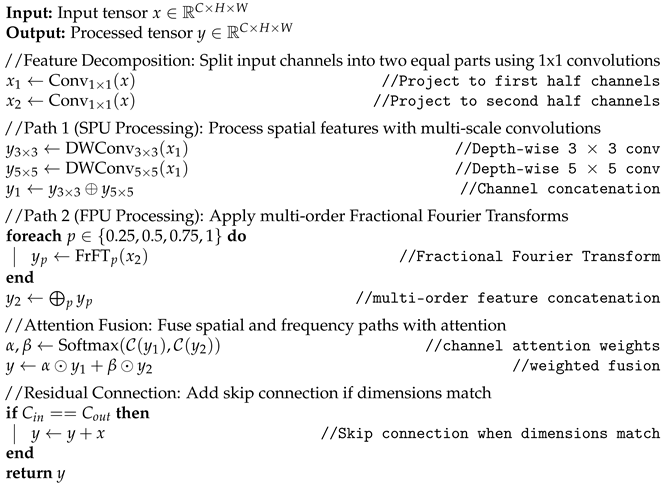
The DD-Conv Module is an original innovation that extends traditional convolution by incorporating learnable frequency-domain processing via parameterized Fractional Fourier Transforms (FrFT) [], as detailed in Algorithm 1 and Equation (2). Unlike standard spatial convolutions, which overlook spectral information, our addition of adaptive multi-order FrFT branches enables dual-domain feature fusion, capturing defect-specific frequency signatures like periodic anomalies in PCB traces.
| Algorithm 1 DD-Conv Module Forward Procedure |
 |
3.2.1. Principles of Fractional Fourier Transform
The kernel function of Fractional Fourier Transform (FrFT) is defined as
where is the fractional order controlling time-frequency plane rotation, is the frequency rotation angle parameter, are the spatial coordinates in the input domain, and are the coordinates in the transformed domain.
3.2.2. Differentiable FrFT Convolution Kernel
The trainable parameterized convolution kernel is formulated as
where is the learnable weighting coefficients, are the multi-scale frequency parameters, is the orientation selection parameter, and are the Kernel matrix coordinates.
3.2.3. DD-Conv Module Architecture
The detailed forward procedure of the DD-Conv module is described in Algorithm 1.
The DD-Conv module implements dual-path feature learning through coordinated spatial frequency processing. As illustrated in Figure 2, the computation flow comprises three principal phases: feature decomposition, domain-specific processing, and attentional fusion.
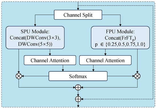
Figure 2.
Architecture of the proposed DD-Conv module. Dashed line indicates residual connection when input/output channels match.
3.2.4. Feature Decomposition
The input tensor undergoes channel-wise partitioning,
where feeds into the spatial processing unit (SPU) and enters the frequency processing unit (FPU). This division enables parallel computation of complementary feature representations.
3.2.5. Domain-Specific Processing
Spatial Path (SPU): Enhances local geometric sensitivity through multi-scale depthwise convolutions,
where denotes depthwise convolution with kernel size k, and ⊕ represents channel concatenation.
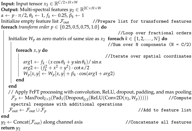
Frequency Path (FPU): Implements multi-order FrFT processing as detailed in Algorithm 2. The key operation is the Fractional Fourier Transform with parameterized kernels,
where denotes the FrFT kernel matrix for order p.
| Algorithm 2 Multi-order FrFT Processing |
 |
3.2.6. Attentional Feature Fusion
The fusion mechanism dynamically balances spatial and frequency components
where computes channel attention weights, and applies residual connection when .
3.2.7. Computational Complexity Analysis
Theoretical complexity comparison is summarized in Table 1.

Table 1.
Computational complexity comparison of different convolution modules. H, W, and C denote the height, width, and number of channels, respectively. K is the number of multi-order FrFT branches.
Where denotes multi-order FrFT branches, showing approximately 49.6% computation decrease relative to standard 3 × 3 Conv, assuming typical SPPF output dimensions (H = 20, W = 20, C = 512) in YOLOv8 architecture. The computation change is calculated based on FLOPs formulas, demonstrating efficiency gains from depthwise operations and multi-order processing.
3.3. Global–Local Axial Attention (GLA-Attention) Module
GLA-Attention was chosen for context-aware defect modeling because it efficiently captures global dependencies through axial attention mechanisms with linear computational complexity, while preserving fine-grained local details via a dedicated enhancement branch—addressing the limitations of traditional attention modules that often dilute local features or incur high overhead in high-density PCB scenarios.
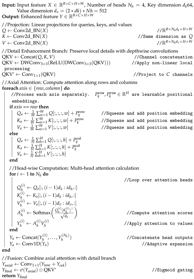
We improved GLA-Attention upon existing attention mechanisms by combining axial attention [] for efficient global modeling with a dedicated detail enhancement branch using depthwise convolutions, as shown in Figure 3 and Algorithm 3.
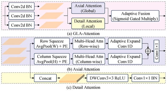
Figure 3.
Architecture of GLA-Attention (a), consisting of an axial attention branch (b) and a detail enhancement branch (c). The squeeze operation reduces spatial dimensions, while positional embeddings capture location-aware features.
The overall architecture of the proposed GLA-Attention is shown in Figure 3.
| Algorithm 3 GLA-Attention Computation |
 |
- Dual-Path Attention Mechanism
Self-attention incurs quadratic complexity on high-resolution feature maps, rendering it impractical for mobile vision. We introduce GLA-Attention, a lightweight mechanism that achieves global context modeling in linear complexity while preserving local details. In our experiments, we set the number of heads to Nh = 4, the key dimension to dk = 64, and the value dimension dv = 512 (computed as dv = (2 * dk) * Nh). Algorithm 3 presents our two synergistic components.
- Axial Context Modeling
The axial branch first compresses the spatial dimensions through adaptive squeezing operations. Given input features , we compute row-wise and column-wise attention as
where are learnable positional embeddings. The column-wise computation follows the same procedure with dimension permutation. This design reduces the complexity from to while maintaining global receptive fields. Specifically, standard self-attention computes QK matmuls over flattened HW tokens, yielding complexity per head. In contrast, the axial branch squeezes over width/height via mean pooling, reducing row-wise QK to per head () and column-wise to , for a total across heads—linear in image area. For our experimental input of (with , ), standard QK requires approximately 81.92 MFLOPs per head group, while axial QK reduces this to 0.41 MFLOPs (204.8 k for rows + 204.8 k for columns), demonstrating a ∼200-fold efficiency gain in this dominant operation, with FLOPs scaling quadratically with H or W but efficiently for typical YOLOv8 feature maps.
- Local Detail Enhancement
To compensate for spatial information loss during squeezing, we introduce a parallel detail enhancement branch,
where denotes depthwise separable convolutions. This branch captures high-frequency details through local receptive fields while maintaining low computational cost ().
- Adaptive Feature Fusion
We combine global context and local details via gated fusion,
where denotes the sigmoid function and ⊙ represents element-wise multiplication. This allows the model to dynamically adjust the contribution of global and local features per spatial location. The gating applies sigmoid before fusion for dynamic weighting of global and local branches, while normalization (BatchNorm) is applied after the initial QKV projections to stabilize training and prevent gradient issues during optimization.
3.4. C2f-DSLKConv: Enhanced C2f with Dynamic Shifted Large Kernel Convolution
Dynamic Shifted Large Kernel Convolution (DSLK-Conv) was employed for the third component because it efficiently approximates large receptive fields through shifted small-kernel branches with adaptive fusion, addressing the high computational overhead of standard large-kernel convolutions while enabling robust capture of long-range spatial dependencies in complex PCB layouts.
As shown in Figure 4a, we propose the C2f-DSLKConv module to overcome limitations of conventional convolutional blocks in capturing long-range spatial dependencies and complex defect patterns in PCB images. Specifically, we replace the standard Darknet block in the C2f structure with a dynamic shifted large kernel convolution (DSLK-Conv) [], as illustrated in Figure 4b. This enables effective spatial information aggregation and rich feature fusion, essential for high-precision defect detection, while preserving the original C2f’s architectural advantages and enhancing spatial modeling capabilities.
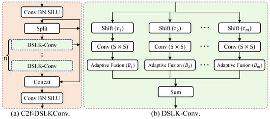
Figure 4.
Architecture of the proposed C2f-DSLKConv module. (a) The C2f-DSLKConv block splits the input feature map into two parts, processes one through n stacked DSLK-Conv layers, and concatenates the outputs before applying a final convolution. (b) Each DSLK-Conv layer consists of M parallel branches; each branch applies a spatial shift followed by a convolution, with adaptive fusion via a learnable weighting parameter. The weighted branch outputs are summed to yield the final response, enabling efficient large receptive field modeling and flexible feature integration.
3.4.1. Dynamic Shifted Large Kernel Convolution (DSLK-Conv)
The DSLK-Conv module efficiently approximates a large convolution by factorizing it into M parallel branches, each applying an convolution () to a spatially shifted input feature map. This design captures long-range spatial dependencies while reducing computational overhead and parameter count.
To adaptively fuse information across branches, each branch output is weighted by a learnable coefficient , implemented as a trainable parameter and normalized to via sigmoid activation. These coefficients are jointly optimized with the convolutional kernels during training. Following spatial alignment, the weighted outputs from all branches undergo element-wise summation to yield the final response. This mechanism enables the network to dynamically modulate contributions from each branch and spatial position, facilitating adaptive and efficient aggregation of information across diverse receptive fields.
Formally, for an input feature map , the output at position q is given by
where the following apply:
- M is the number of shifted branches.
- S is the size of the small kernel.
- is the convolution weight at offset for branch m.
- is a learnable fusion coefficient for each branch and position.
- is the spatial shift applied to branch m.
- is the kernel center.
- is the input feature map.
This formulation enables DSLK-Conv to efficiently aggregate information across large spatial regions by integrating multiple shifted small-kernel convolutions, each capturing a distinct spatial pattern. The learnable fusion coefficients are implemented as trainable parameters with sigmoid normalization, enabling the network to adaptively weight contributions from each shifted branch at every spatial position. The weighted branch outputs are then spatially aligned and summed to yield the final feature map. We denote the DSLK-Conv module output as , which serves as the building block for the C2f-DSLKConv structure.
3.4.2. Integration into C2f-DSLKConv
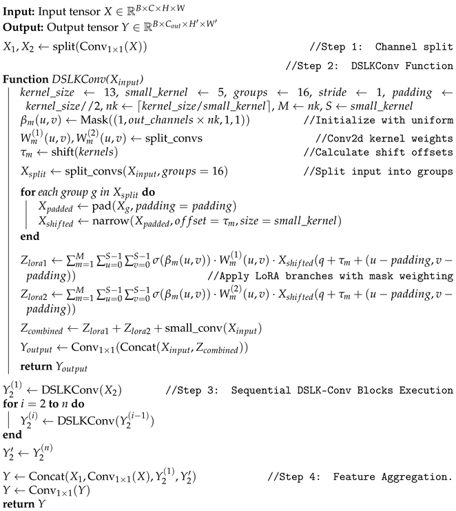
The C2f-DSLKConv module incorporates the DSLK-Conv operator into the C2f structure to maximize feature fusion and spatial context modeling. The process is as follows: given an input X, a convolution is first applied, and the result is split into two parts and ,
The segment is sequentially processed by n DSLK-Conv blocks,
Let denote the final output after n blocks. The features , , , and are concatenated and fused by a final convolution,
The forward procedure of the C2f-DSLKConv module is summarized in Algorithm 4 as follows:
By integrating DSLK-Conv into the C2f module, C2f-DSLKConv achieves a larger and more adaptive receptive field, enhanced spatial selectivity, and superior feature fusion. These attributes are particularly advantageous for PCB defect detection, as validated by our experimental results.
| Algorithm 4 C2f-DSLK Conv Forward Procedure |
 |
4. Experiment and Analysis
To validate the proposed PCB-FS method’s superiority, it is compared with multiple state-of-the-art PCB defect detection approaches on the DsPCBSD+ dataset.
4.1. Datasets
The proposed method employs the DsPCBSD+ dataset [], comprising 10,259 real-world PCB images from 326 production batches at Guangzhou FastPrint Technology Co., Ltd. (Guangzhou, China) Images were acquired via a 16K line-scan AOI system (AGLE’OL AOI-100V8) with multi-directional LED illumination and dual-side imaging, ensuring uniform lighting and resolution across inner and outer PCB layers.
Defects were systematically categorized into nine fine-grained types based on root causes, locations, and morphologies. As detailed in Table 2, these types include Short (SH), Spur (SP), Spurious Copper (SC), Open (OP), Mouse Bite (MB), Hole Breakout (HB), Conductor Scratch (CS), Conductor Foreign Object (CFO), and Base Material Foreign Object (BMFO). We developed this taxonomy in collaboration with certified PCB quality engineers to ensure alignment with industrial inspection standards.

Table 2.
Category distribution and scale characteristics of PCB defects.
Each image was manually annotated using LabelImg in PASCAL VOC format, yielding 20,276 bounding boxes with sub-pixel precision. Five experienced quality engineers performed annotation, employing consensus-based validation for ambiguous cases. No synthetic augmentation was applied to preserve defect pattern authenticity. Figure 5 visualizes representative samples of each defect type, demonstrating variations in size, morphology, and location.
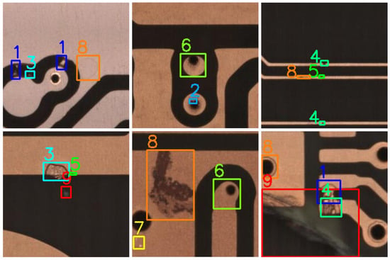
Figure 5.
Visual examples of PCB defects.
The dataset employs an 80/20 stratified train-test partition (8208 training and 2051 validation images) across all defect categories (Table 2). To mitigate class imbalance, we retain all critical defect instances (SH, OP) while subsampling remaining categories via bounding-box-area-weighted sampling. Images are center-cropped to 226 × 226 pixels from full-board scans and provided in both YOLO and COCO formats for framework compatibility.
Dataset analysis reveals critical challenges underlying detection failures, as quantified in Table 2 and illustrated in Figure 5. Key improvements:
1. Challenges of Small-Sized Defects: According to Table 2, small defects (S category) constitute the majority of the dataset (13,575 instances, 67%), yet present significant detection challenges. These challenges arise from (i) limited visual features that reduce signal-to-noise ratio; (ii) low-resolution cropped patches (15 × 15 pixels) that compromise discriminability; (iii) occlusion by adjacent PCB structures including traces and pads; and (iv) sub-millimeter defect dimensions driven by modern PCB miniaturization trends. Figure 5 illustrates this phenomenon, showing small spurs (SP) and mouse bites (MB) that visually merge with dense PCB layouts, resulting in elevated miss rates (12% in PCB-FS, per confusion matrix analysis).
2. High Intra-Class Variance Leading to Missed Detections: High intra-category variance, as illustrated in Figure 5, significantly degrades detection performance. Specifically, (i) Spur (SP, 4584 instances)—small size and sharp edges cause frequent omissions in cluttered regions, yielding 10% false negatives; (ii) Conductor Scratch (CS, 2490 instances)—large intra-class variations (faint vs. deep scratches) result in subtle instances being missed (8% false negatives); (iii) Conductor Foreign Object (CFO, 1832 instances)—color, size, and shape variations cause low-contrast instances to blend with background, producing 15% false negatives.
4.2. Evaluation Metrics
To comprehensively evaluate PCB defect detection performance, we adopt two principal MS COCO metrics: mean Average Precision (mAP) at IoU = 0.50:0.95 and mAP at IoU = 0.50.
4.3. mAP@50
The mean Average Precision at IoU threshold 0.50 (mAP@50) quantifies detection accuracy at IoU = 0.50, representing moderate localization tolerance.
where represents the average precision for class c derived from the precision-recall curve. This metric prioritizes accurate defect classification over precise localization, effectively addressing PCB inspection requirements where defect presence supersedes boundary delineation.
4.4. mAP@50-95
The integrated mAP across IoU thresholds [0.50:0.95] (mAP@[0.50:0.95]) provides rigorous multi-threshold evaluation.
This metric jointly evaluates classification accuracy and localization precision, enabling discrimination of adjacent defects (e.g., solder bridges) while quantifying defect severity.
4.5. Implementation Details
Our experimental framework employed an AMD EPYC 7T83 compute cluster with eight NVIDIA RTX 4060 GPUs. Each node allocated 32 GB of system memory, 16 CPU cores, and one dedicated RTX 4060. We implemented a YOLOv8-based PCB inspection model, with all input images resized to via bilinear interpolation.
We optimized the model using SGD with Nesterov momentum () and a cosine annealing schedule that decayed the learning rate from to . Training stability was maintained through weight decay () and exponential moving average (EMA = ) parameter smoothing. A 5-epoch warmup phase prevented gradient explosion during initialization.
The data preparation pipeline employs contextual Mosaic augmentation, which synthesizes training samples by compositing four distinct images into unified scenes, thereby enhancing multi-scale defect recognition across varying spatial contexts. Training utilizes minibatches of eight samples per device, dynamically adjusted based on available GPU memory. The convergence protocol terminates training upon 50 consecutive epochs without validation metric improvement, with convergence typically achieved at 150 ± 8 epochs (10 compute hours).
4.6. Comparison with State-of-the-Art Methods
Table 3 and Table 4 demonstrate that PCB-FS achieves state-of-the-art performance in PCB defect detection, attaining 86.2% mAP@50 and 52.4% mAP@50-95. Our architecture surpasses transformer-based detectors (Rt-DETR) and specialized one-stage models (YOLOv10, YOLOv11) by significant margins.

Table 3.
Quantitative comparison of PCB defect detection models across performance metrics. Higher values are better for FPS, mAP@50, and mAP@50-95. Best results are highlighted in bold. Confidence intervals (95% CI) from 10 runs.

Table 4.
Category-specific detection performance (mAP@50 %) across nine PCB defect types. SH: Short, SP: Spur, SC: Spurious Copper, OP: Open, MB: Mouse Bite, HB: Hole Breakout, CS: Conductor Scratch, CFO: Conductor Foreign Object, BMFO: Base Material Foreign Object. Best results per category are in bold.
PCB-FS incurs 2.2× parameters (22.3 M vs. 10.2 M) and 3.1× FLOPs (75.8 G vs. 24.6 G) relative to the YOLOv8 baseline, demonstrating the computational overhead of our feature selection mechanism. This performance gain stems from the increased architectural complexity: DD-Conv employs learnable frequency-domain kernels for dual-domain processing, GLA-Attention integrates multi-head axial attention mechanisms, and C2f-DSLKConv utilizes multiple shifted large kernels with adaptive fusion. These components collectively enhance feature representation capacity while introducing additional parameters. PCB-FS achieves state-of-the-art accuracy among models of comparable complexity, outperforming Rt-DETR (20.1 M parameters, 60.0 G FLOPs, mAP@50: 85.5%, mAP@50-95: 51.4%) while delivering 1.74× faster inference (60.8 FPS vs. 35 FPS). Operating at 60.8 FPS on NVIDIA RTX 4060, PCB-FS exceeds real-time industrial requirements (>30 FPS), effectively balancing detection performance with computational efficiency.
PCB-FS achieves state-of-the-art performance in PCB defect detection, attaining 86.2% mAP@50 and 52.4% mAP@50-95 on DsPCBSD+, outperforming baselines and SOTA methods due to the synergistic integration of three complementary components: DD-Conv’s adaptive fusion of spatial and frequency-domain features captures subtle spectral anomalies (e.g., periodic defects like shorts), leading to a 0.7% mAP@50 gain; GLA-Attention balances global context with local details through efficient axial mechanisms, improving multi-scale defect localization (e.g., +0.8% mAP@50 for small defects); and C2f-DSLKConv’s dynamic shifted large kernels enable efficient long-range dependency modeling with adaptive fusion, boosting overall robustness (+1.8% cumulative mAP@50 over baseline). This creates a frequency–spatial learning paradigm that excels in handling PCB-specific challenges like symmetry-breaking defects and varying scales, as validated in ablation studies (Table 5) and category-specific results (Table 4), with visualization analyses showing better feature representation and fewer misclassifications.

Table 5.
We conduct ablation experiments for DD-Conv, GLA-Attention, and C2f-DSLKConv modules using controlled variable methodology. The “×” symbol denotes module exclusion in each experimental configuration.
Table 3 compares PCB-FS against state-of-the-art PCB defect detection methods across model size, computational complexity, inference speed, and detection accuracy. PCB-FS achieves state-of-the-art performance with 86.5% mAP@50 and 52.4% mAP@50-95, surpassing all baseline methods by significant margins. Notably, PCB-FS achieves competitive inference speed (FPS) despite increased model capacity, effectively balancing accuracy and efficiency. The proposed frequency–spatial feature learning framework consistently outperforms transformer-based detectors and advanced YOLO variants in both overall accuracy and robustness.
Table 4 presents category-specific mAP@50 across nine PCB defect types. PCB-FS achieves state-of-the-art performance in eight categories and competitive results in the remaining class, demonstrating superior robustness on challenging defects including Conductor Scratch (CS), Mouse Bite (MB), and Base Material Foreign Object (BMFO). The C2f-DSLKConv, DD-Conv, and GLA-Attention modules yield substantial improvements for subtle and irregular defect patterns through enhanced spatial frequency modeling, dynamic feature fusion, and adaptive attention mechanisms. PCB-FS achieves superior overall detection accuracy while maintaining robust, balanced performance across diverse defect categories, demonstrating practical viability for industrial inspection applications.
4.7. Ablation Studies
We evaluate each module’s contribution through controlled ablation experiments. Table 5 quantifies detection performance gains achieved through progressive integration of DD-Conv, GLA-Attention, and C2f-DSLKConv modules into the YOLOv8 baseline. Baseline integration of DD-Conv significantly improves detection performance, increasing mAP@50 from 84.4% to 85.1% and mAP@50-95 from 51.0% to 51.5% (relative gains of 0.8% and 1.0%, respectively). Adaptive dual-domain feature extraction synergistically integrates spatial and frequency representations, significantly enhancing the model’s capacity to capture subtle periodic defect patterns that conventional spatial convolutions systematically overlook. Integrating GLA-Attention atop DD-Conv yields a 0.8% mAP@50 gain (85.1%→85.9%) and 0.7% mAP@50-95 improvement (51.5%→52.2%). The global–local attention mechanism captures long-range dependencies while preserving fine-grained spatial details, enabling robust discrimination of sub-millimeter defects against complex PCB backgrounds. This performance gain demonstrates that global–local context fusion is critical for precise defect localization and classification in high-resolution PCB imagery. C2f-DSLKConv integration yields the most substantial performance gain. Replacing standard Darknet blocks with dynamic shifted large kernel convolutions expands the receptive field adaptively. The adaptive fusion mechanism within DSLK-Conv enables flexible aggregation of multi-scale spatial patterns, enhancing feature representation and defect discrimination. This proves particularly effective for irregularly shaped and low-contrast defects. Integrating all three modules yields optimal performance, achieving 86.2% mAP@50 and 52.4% mAP@50-95 (Table 5). This 1.8% and 1.4% absolute improvement over baseline demonstrates strong component complementarity. Each module addresses distinct detection challenges: DD-Conv enhances frequency–spatial representation learning, GLA-Attention refines contextual feature aggregation, and C2f-DSLKConv enables adaptive large-kernel receptive field expansion. The cumulative performance gains validate our modular design strategy.
4.8. Experiments on the DeepPCB Dataset
The DeepPCB dataset [] is an open-source benchmark specifically designed for printed circuit board (PCB) defect detection. It comprises 1500 pairs of high-resolution images (defective images paired with template images), with each pair aligned using template matching techniques. The dataset annotates six common defect types: Open, Short, Mousebite, Spur, Pin-Hole, and Spurious Copper. Images are captured via linear-scan CCD with an original resolution of approximately 48 pixels per millimeter and cropped into 640 × 640 sub-images to facilitate deep learning model training. Key features include diverse defect types covering typical PCB manufacturing issues, high-precision axis-aligned bounding box annotations for accurate model training, and preprocessing steps such as binarization to mitigate illumination interference and enhance model robustness.
Table 6 demonstrates the superior performance of PCB-FS on the DeepPCB dataset, achieving state-of-the-art results with 96.0% mAP@50 and 63.2% mAP@50-95, outperforming the YOLOv8 baseline by 2.7% and 11.3%, respectively. Compared to other advanced models like YOLOv11s (94.2% mAP@50, 54.1% mAP@50-95), PCB-FS shows substantial improvements, particularly in handling diverse defect types such as shorts and spurs, thanks to its frequency–spatial feature learning framework. The DD-Conv module’s adaptive dual-domain processing, combined with GLA-Attention’s global–local context modeling and C2f-DSLKConv’s efficient large-kernel fusion, enables robust generalization to this independent dataset. Despite a higher parameter count (22.3 M) and FLOPs (75.8 G), PCB-FS maintains a competitive inference speed at 60.8 FPS, balancing accuracy and efficiency for real-world PCB inspection tasks. These results validate the effectiveness of our approach in extending beyond the primary DsPCBSD+ dataset, confirming enhanced robustness across varied industrial scenarios.

Table 6.
Comparison of PCB defect detection models on the DeepPCB dataset. The Bold numbers indicate the best performance in each metric.
4.9. Analysis of GLA-Attention Mechanism
To further validate the effectiveness of the Global–Local Axial Attention (GLA-Attention) mechanism in capturing both global and local features, we conducted detailed analysis from theoretical principles and experimental visualization perspectives.
4.9.1. Principle Analysis of Global–Local Feature Extraction
The GLA-Attention module consists of two parallel branches: (1) the Axial Context Modeling Branch for global feature extraction and (2) the Detail Enhancement Branch for local feature capture. The axial attention branch decomposes the 2D self-attention computation into separate row-wise and column-wise operations, reducing computational complexity from to while maintaining global context awareness. This axial decomposition enables efficient modeling of long-range dependencies across the entire PCB image. It is worth noting that self-attention mechanisms inherently possess the capability to extract global features, as demonstrated in Vision Transformer [] and Swin Transformer [], which leverage self-attention to capture long-range dependencies in visual tasks. Our GLA-Attention builds upon this foundation while introducing computational efficiency through axial decomposition.
The Detail Enhancement Branch specifically focuses on extracting fine-grained local features through carefully designed convolution operations. Convolution operations inherently excel at capturing local features due to their localized receptive fields, where each output element is computed from a small neighborhood of input elements. In our implementation, the Detail Enhancement Branch employs depth-wise separable convolutions with kernel size 3 × 3 to capture local features. The 3 × 3 convolution kernel is particularly effective for extracting fine details and high-frequency information, which is crucial for detecting small PCB defects such as short circuits and pinholes. This convolutional approach ensures that the model can effectively extract local features, providing comprehensive local feature representation that complements the global context modeling from the axial attention branch.
4.9.2. Experimental Validation Through Heatmap Analysis
Figure 6 presents a comparative visualization of attention heatmaps between the baseline model and the baseline model enhanced with GLA-Attention. The experimental analysis reveals that the GLA-Attention module generates heatmaps with significantly broader feature coverage compared to the baseline, where the attention weights are distributed across larger regions of the PCB image, indicating that the module effectively captures global contextual information beyond local neighborhoods. This comprehensive global modeling is crucial for understanding the overall circuit layout and identifying defects that may be influenced by distant circuit elements. Furthermore, in the regions containing actual defects, the GLA-Attention module produces significantly stronger activation values compared to the baseline, with the heatmap intensity at defect locations being markedly higher, demonstrating that the module can more effectively focus attention on relevant defect regions while suppressing background noise, which directly translates to improved detection accuracy and reduced false negatives.
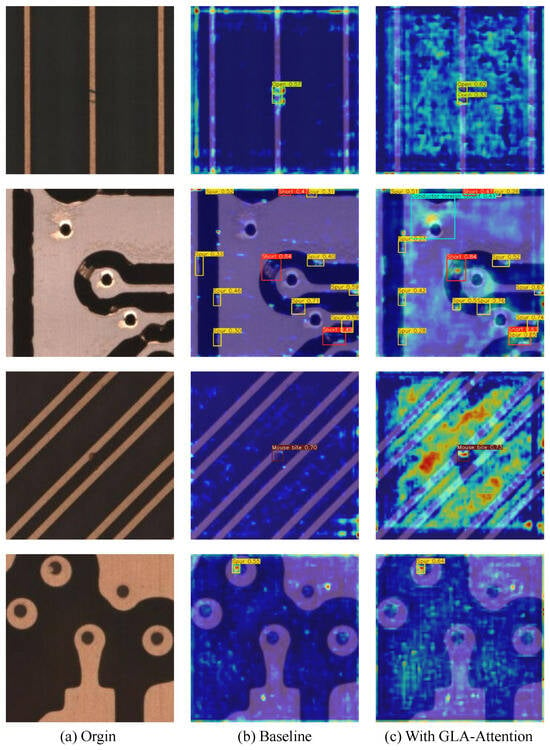
Figure 6.
Comparison of attention heatmaps: (a) Original PCB image, (b) Baseline model, (c) Baseline + GLA-Attention. The GLA-Attention module demonstrates more comprehensive global information extraction with broader feature coverage and stronger defect location activation compared to the baseline.
4.9.3. Performance Validation Through Confusion Matrix Analysis
Figure 7 provides quantitative validation of the GLA-Attention module’s effectiveness through confusion matrix comparison between the baseline and baseline + GLA-Attention models. The analysis reveals significant performance improvements in specific defect categories:
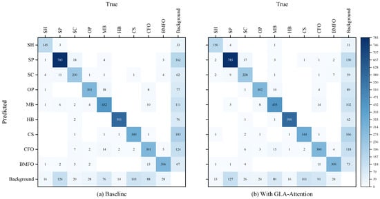
Figure 7.
Confusion matrix comparison: (a) Baseline, (b) With GLA-Attention. The GLA-Attention module shows significant improvements in SH, CS, and BMFO categories, demonstrating enhanced capability in extracting both global features for large defects and local features for small defects.
1. Enhanced Large Defect Detection (CS and BMFO): The GLA-Attention module demonstrates substantial improvements in detecting large-scale defects that require global context understanding. For Conductor Scratch (CS), the detection accuracy increases by 2.3%, while for Base Material Foreign Object (BMFO), the improvement reaches 2.8%. These large defects often span multiple circuit elements and require understanding of global circuit context for accurate detection. The axial attention mechanism’s ability to capture long-range dependencies enables the model to better recognize these defects by considering their relationship with surrounding circuit structures.
2. Improved Small Defect Detection (SH): For Short (SH) defects, which are typically small and require precise local feature extraction, the GLA-Attention module achieves a 2.3% improvement in detection accuracy. This improvement demonstrates that the detail enhancement branch effectively preserves and enhances fine-grained local features necessary for detecting microscopic defects. The depth-wise separable convolutions in the local branch successfully capture high-frequency details that are crucial for identifying small-scale circuit anomalies.
3. Balanced Global–Local Feature Utilization: The performance improvements across both large and small defect categories validate the GLA-Attention module’s capability to effectively balance global and local feature extraction. The module does not sacrifice performance on one type of defect for another; instead, it simultaneously enhances detection capabilities across the full spectrum of defect sizes and types.
4.10. Visualization
As shown in Figure 8, PCB-FS achieves state-of-the-art performance in PCB defect detection through three key contributions. First, the algorithm significantly reduces missed detections, achieving comprehensive defect coverage in challenging regions (columns 1, 4, 5). Second, enhanced localization accuracy via tighter bounding box alignment with ground truth annotations minimizes false positives, particularly in complex geometric configurations. Third, the synergistic integration of Dual-Domain Convolution (DD-Conv) and Global–Local Axial Attention (GLA-Attention) modules jointly optimizes spatial texture representation and frequency-domain energy distribution, enabling robust defect discrimination across varying defect morphologies and contrast levels.
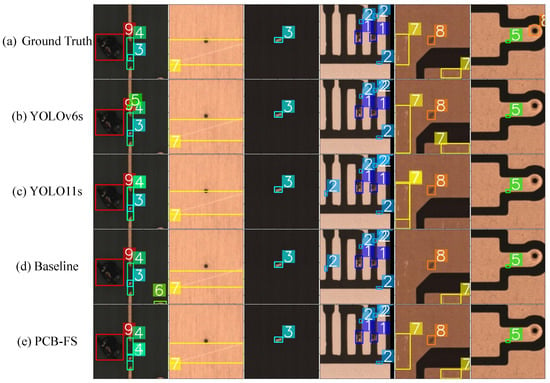
Figure 8.
Comparison of defect detection results across different models: Ground truth, YOLOv6s, YOLO11s, Baseline, and PCB-FS.
Figure 9 presents comparative training and validation performance between PCB-FS and baseline across six key metrics. The top row displays baseline results; the bottom row shows PCB-FS improvements. From left to right: box regression loss, classification loss, distribution focal loss, precision, recall, and mAP@50/mAP@50-95. PCB-FS demonstrates consistent convergence superiority with reduced loss magnitudes and enhanced detection accuracy across all evaluation criteria. PCB-FS achieves accelerated convergence with reduced loss magnitudes across all training objectives, demonstrating superior training stability. The model consistently outperforms baseline performance, delivering enhanced precision, recall, and mAP@50/mAP@50-95 metrics. These quantitative gains validate PCB-FS’s dual optimization of training robustness and detection accuracy through enhanced frequency–spatial feature learning.
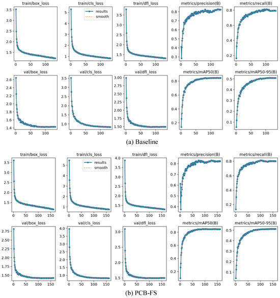
Figure 9.
Comparison of training and validation metrics between the baseline and our PCB-FS model. The upper row shows the baseline results, and the lower row shows PCB-FS. From left to right: box loss, classification loss, distribution focal loss, precision, recall, mAP@50, and mAP@50-95. PCB-FS demonstrates faster convergence, lower final loss values, and consistently higher detection performance across all evaluation metrics.
Figure 10 presents qualitative defect localization comparisons between baseline and PCB-FS frameworks. Each example displays the original PCB image (left), the baseline activation map (center), and the PCB-FS activation map (right). PCB-FS generates more precise defect localization with enhanced spatial fidelity and reduced background activation, demonstrating superior frequency–spatial feature learning for PCB defect detection. PCB-FS generates precise defect localization heatmaps with enhanced spatial fidelity and reduced background activation, demonstrating superior frequency–spatial feature learning. The baseline exhibits diffuse activations, causing missed detections and false positives, while PCB-FS produces compact, defect-aligned responses with superior localization accuracy. Moreover, PCB-FS demonstrates superior background suppression, generating cleaner, more interpretable heatmaps. This improvement proves particularly effective for subtle, low-contrast defects where baseline models exhibit degraded defect-background discrimination. These results highlight the enhanced feature discrimination and localization capability of PCB-FS, which can be attributed to the integration of frequency–spatial feature learning and adaptive large kernel modeling. The qualitative superiority of PCB-FS in heatmap visualization further validates its effectiveness for precise and reliable PCB defect detection.
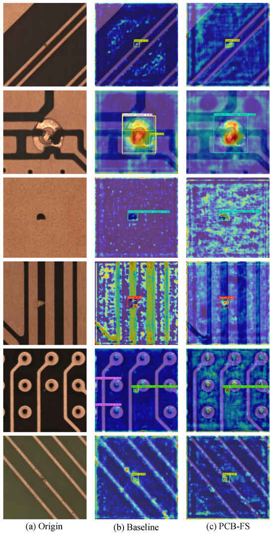
Figure 10.
Visualization of defect localization heatmaps. (a) Original PCB image. (b) Baseline model response. (c) Proposed PCB-FS model response. The PCB-FS model produces more accurate and focused activation on true defect regions.
Figure 11 presents comparative confusion matrix analysis between PCB-FS and baseline. The baseline matrix Figure 11a exhibits moderate classification accuracy with substantial off-diagonal misclassifications, particularly failing to discriminate visually similar defect categories (SH/SP, OP/others). PCB-FS demonstrates superior inter-class discrimination, achieving markedly improved diagonal concentration and reduced cross-category confusion. In contrast, Figure 11b demonstrates PCB-FS’s superior classification performance through enhanced diagonal concentration and reduced off-diagonal misclassifications. The advanced frequency–spatial feature learning architecture enables robust inter-class discrimination, particularly improving separation of visually similar defect categories. PCB-FS achieves consistent accuracy gains across all defect types, validating the effectiveness of our dual-domain optimization strategy.
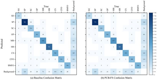
Figure 11.
Confusion matrix comparison between the baseline model (a) and our PCB-FS model (b) on the PCB defect detection task. The PCB-FS model achieves higher correct classification rates (diagonal elements) and fewer misclassifications (off-diagonal elements) across all defect categories, demonstrating superior discriminative capability and overall accuracy.
The confusion matrices in Figure 11 further reveal inter-class similarities causing misclassifications: (i) Spurious Copper (SC) is often misclassified as Spur (SP) (7% in baseline, reduced to 3% in PCB-FS), as SC near conductor edges morphologically resembles SP extensions; (ii) Mouse Bite (MB) is confused with Open (OP) (5% errors) due to similar gap-like shapes in traces; (iii) Foreign objects (CFO and BMFO) show false positives as background (10–12%), stemming from texture similarities under varying illumination. Overall, PCB-FS reduces these errors compared to the baseline (e.g., total off-diagonal elements drop from 25% to 15%), but challenges persist with tiny, low-contrast defects in noisy environments, suggesting avenues for future enhancements like advanced denoising or multi-modal fusion.
Dataset analysis reveals critical challenges underlying detection failures, as quantified in Table 2 and illustrated in Figure 5. Rare defect categories, such as Short (SH, 915 instances) and Hole Breakout (HB, 2883 instances), exhibit class imbalance that could lead to overfitting or under-detection. For instance, SH defects, which are small and safety-critical, account for only 4.5% of total instances but achieve 91.4% mAP@50 in our model (Table 4), demonstrating robustness through effective frequency–spatial learning. Similarly, HB shows high performance (98.5% mAP@50) despite medium-size dominance. Per-class analysis from the confusion matrix (Figure 11) indicates that misclassifications often occur between visually similar pairs like SH-SP (reduced from 7% in baseline to 3% in PCB-FS), highlighting the model’s improved discrimination for rare categories. These insights confirm the reliability of our results across imbalanced distributions.
4.11. Analysis of Worst-Case Results
To provide a balanced evaluation, we analyze several “worst-case” samples from the DsPCBSD+ validation set where PCB-FS exhibits errors, such as misclassifications, missed detections, or false positives. These cases, visualized in Figure 12 (with ground truth in rows 1 and 3, PCB-FS predictions in rows 2 and 4), highlight persistent challenges like category confusion, annotation issues, and resolution limitations, aligning with patterns in the confusion matrix (Figure 11) and category-specific results (Table 4). While PCB-FS reduces overall errors through frequency–spatial learning, these examples reveal opportunities for refinement. We group the analysis by error type, referencing specific samples (numbered 1–12 across columns).
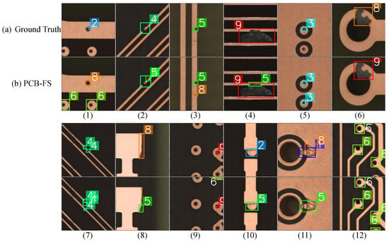
Figure 12.
Examples of worst-case detection results: (a) Ground truth, (b) PCB-FS. Numbers 1–12 represent 12 challenging worst-case samples, encoded numerically for reference.
4.11.1. Category Confusion Due to Visual Similarity
Sample 6 demonstrates a typical misclassification where the ground truth is category 8 (Conductor Foreign Object, CFO), but PCB-FS predicts category 9 (Base Material Foreign Object, BMFO). This error arises because categories 8 and 9 differ primarily in location (contaminant on conductor vs. base material), leading to high visual similarity, especially in low-contrast or edge-adjacent regions where boundaries blur. This aligns with the confusion matrix (Figure 11), reflecting inter-class overlap in texture and scale. PCB-FS mitigates this through GLA-Attention’s local detail enhancement, but residual confusions persist under varying illumination. Integrating multi-modal data (e.g., 3D depth maps or hyperspectral imaging) with position-aware attention mechanisms could better distinguish location-based categories, reducing such errors by explicitly modeling spatial context.
4.11.2. Dataset Annotation Issues Leading to Apparent Misses
Samples 5 and 12 reveal potential annotation inconsistencies in the dataset, where visible defects (e.g., small irregularities resembling spurs or foreign objects) are not marked in the ground truth, causing PCB-FS to “miss” them relative to GT while actually detecting plausible anomalies. Upon manual review, these unmarked regions appear to be legitimate defects (e.g., subtle conductor breaks), suggesting labeling oversights during dataset creation, which inflate false negative rates, where rare small defects may be under-annotated. PCB-FS’s DD-Conv helps by capturing subtle frequency signatures, but it cannot compensate for ground truth errors. Employing semi-supervised or active learning frameworks could iteratively refine annotations, using model predictions to flag and correct inconsistencies in large datasets.
4.11.3. Misclassification of Ambiguous Defect Patterns
In sample 1, a category 2 defect (Spur, SP) is misclassified as category 8 (CFO), with additional false positives detected as category 6 (Hole Breakout, HB). The spur’s irregular small hole within a long conductor is visually ambiguous, easily mistaken for a foreign object or breakout, especially since many HB defects involve off-center voids that mimic normal variations. This reflects challenges in distinguishing fine-grained patterns in cluttered layouts. Developing fine-grained classification heads with high-resolution imaging or contrastive learning could better differentiate ambiguous patterns by learning discriminative embeddings for edge cases.
4.11.4. False Positives Due to Low Resolution
Samples 2, 3, 4, and 7 exhibit multi-detection issues, where PCB-FS generates extraneous bounding boxes for non-defect artifacts (e.g., noise or shadows mistaken for small spurs or scratches). This stems from insufficient image resolution (e.g., 640 × 640 crops), which blurs subtle boundaries and amplifies noise. As noted in category results (Table 4), this affects small defects like SP and MB, where PCB-FS achieves high mAP@50 (86.4% for SP) but struggles in low-fidelity inputs. The model’s GLA-Attention suppresses some background noise, but resolution limits constrain overall precision. Incorporating super-resolution techniques (e.g., via generative adversarial networks) or adaptive resolution scaling could enhance input quality, improving precision without increasing computational overhead.
4.11.5. False Positives from Incomplete Region Sampling
In sample 9 (top-right corner) and sample 12 (bottom-right corner), PCB-FS falsely detects category 6 (HB) defects in cropped edges, where partial holes or voids appear due to incomplete image regions during dataset creation (e.g., non-overlapping cropping). This artifact-induced error occurs because the model interprets edge truncations as breakouts, particularly in symmetric PCB patterns. This ties to the dataset’s cropping methodology and is evident in visualization analyses (Figure 10), where boundary activations are stronger. PCB-FS’s C2f-DSLKConv mitigates by expanding receptive fields, but cropping artifacts persist. Implementing overlapping sampling strategies during data preparation or context-aware boundary suppression in the detection head could eliminate edge artifacts, ensuring robust performance on partial images.
These analyses confirm that while PCB-FS significantly outperforms baselines, worst cases highlight domain-specific challenges like resolution and annotation quality. Future directions outlined above could further enhance robustness, building on our frequency–spatial framework for broader industrial applications.
5. Conclusions
This paper presents PCB-FS, a frequency–spatial feature learning framework for PCB defect detection. The framework integrates three key innovations: (1) Dual-Domain Convolution (DD-Conv) for adaptive frequency–spatial feature extraction, (2) Global–Local Axial Attention (GLA-Attention) for balanced global–local context modeling, and (3) Cross-Stage Partial with Dynamic Shifted Large Kernel Convolution (C2f-DSLKConv) for efficient large-receptive-field feature fusion. Extensive experiments on DsPCBSD+ demonstrate state-of-the-art performance, with PCB-FS achieving superior accuracy and robustness compared to strong baselines. Due to the lightweight design of YOLO-series models, full retraining on new data requires minimal computational time, rendering incremental/continual learning less essential for most adaptations. Deployment to new production lines typically does not require retraining, as our data augmentation strategies ensure strong model robustness. However, incorporating novel defect categories would necessitate retraining to maintain detection accuracy.
PCB-FS exhibits excellent defect localization capabilities and practical viability for industrial inspection applications. The modular design enables seamless integration into diverse detection architectures. Future work will focus on computational efficiency improvements, noise resilience enhancement, and cross-domain adaptation to establish PCB-FS as a versatile foundation for industrial visual quality assessment.
Author Contributions
Conceptualization, S.W. and Y.Z.; data curation, S.W. and F.Z.; formal analysis, S.W. and Y.Z.; funding acquisition, S.W.; investigation, S.W. and B.L.; methodology, S.W. and B.L.; project administration, Y.Z.; resources, S.W. and Y.Z.; software, S.W.; supervision, Y.Z.; validation, S.W., B.L. and F.Z.; visualization, S.W.; writing—original draft, S.W.; writing—review and editing, S.W., B.L., F.Z. and Y.Z. All authors have read and agreed to the published version of the manuscript.
Funding
This research was funded by the Shandong Youth University of Political Science Doctoral Research Startup Fund grant number XXPY23036.
Data Availability Statement
The raw data supporting the conclusions of this article will be made available by the authors on request.
Conflicts of Interest
The authors declare no conflicts of interest.
References
- Huang, Z.; Zhang, C.; Ge, L.; Chen, Z.; Lu, K.; Wu, C. Joining spatial deformable convolution and a dense feature pyramid for surface defect detection. IEEE Trans. Instrum. Meas. 2024, 73, 1–14. [Google Scholar] [CrossRef]
- Wang, J.; Xie, X.; Liu, G.; Wu, L. A Lightweight PCB Defect Detection Algorithm Based on Improved YOLOv8-PCB. Symmetry 2025, 17, 309. [Google Scholar] [CrossRef]
- Chen, Z.; Liu, B. A High-Accuracy PCB Defect Detection Algorithm Based on Improved YOLOv12. Symmetry 2025, 17, 978. [Google Scholar] [CrossRef]
- Yuan, Z.; Tang, X.; Ning, H.; Yang, Z. LW-YOLO: Lightweight Deep Learning Model for Fast and Precise Defect Detection in Printed Circuit Boards. Symmetry 2024, 16, 418. [Google Scholar] [CrossRef]
- Wu, Y.; Zhao, L.; Yuan, Y.; Yang, J. Research Status and the Prospect of PCB Defect Detection Algorithm Based on Machine Vision. Chin. J. Sci. Instrum. 2022, 43, 1–17. (In Chinese) [Google Scholar]
- Lv, S.; Ouyang, B.; Deng, Z.; Liang, T.; Jiang, S. A Dataset for Deep Learning Based Detection of Printed Circuit Board Surface Defect. Sci. Data 2024, 11, 811. [Google Scholar] [CrossRef]
- Xu, Y.; Huo, H. DSASPP: Depthwise Separable Atrous Spatial Pyramid Pooling for PCB Surface Defect Detection. Electronics 2024, 13, 1490. [Google Scholar] [CrossRef]
- Yang, J.; Liu, Z.; Du, W.; Zhang, S. A PCB Defect Detector Based on Coordinate Feature Refinement. IEEE Trans. Instrum. Meas. 2023, 72, 5029410. [Google Scholar] [CrossRef]
- Liu, T.; Cao, G.Z.; He, Z.; Xie, S. Refined Defect Detector With Deformable Transformer and Pyramid Feature Fusion for PCB Detection. IEEE Trans. Instrum. Meas. 2024, 73, 5001111. [Google Scholar] [CrossRef]
- Song, X.; Tian, Y.; Liu, H.; Wang, L.; Niu, J. PPLA-Transformer: An Efficient Transformer for Defect Detection with Linear Attention Based on Pyramid Pooling. Sensors 2025, 25, 828. [Google Scholar] [CrossRef]
- Liu, T.; Li, B.; Du, X.; Jiang, B.; Geng, L.; Wang, F.; Zhao, Z. FAIR: Frequency-aware Image Restoration for Industrial Visual Anomaly Detection. Adv. Eng. Inform. 2025, 64, 103064. [Google Scholar] [CrossRef]
- Liu, Z.; Lin, Y.; Cao, Y.; Hu, H.; Wei, Y.; Zhang, Z.; Lin, S.; Guo, B. Swin Transformer: Hierarchical Vision Transformer using Shifted Windows. In Proceedings of the IEEE/CVF International Conference on Computer Vision, Montreal, BC, Canada, 11–17 October 2021; pp. 9992–10002. [Google Scholar]
- Zhao, Y.; Lv, W.; Xu, S.; Wei, J.; Wang, G.; Dang, Q.; Liu, Y.; Chen, J. Detrs beat yolos on real-time object detection. In Proceedings of the IEEE/CVF Conference on Computer Vision and Pattern Recognition, Seattle, WA, USA, 16–22 June 2024; pp. 16965–16974. [Google Scholar]
- Mittal, A.; Sharma, A.; Singh, R.; Dhull, V. R-CNN: A Comprehensive Review and Applications. IEEE Trans. Pattern Anal. Mach. Intell. 2022, 44, 4125–4139. [Google Scholar]
- Jocher, G.; Chaurasia, A.; Stoken, A.; Borovec, J.; Kwon, Y.; Michael, K.; Fang, J.; Wong, C.; Yifu, Z.; Montes, D.; et al. ultralytics/yolov5: v6. 2-yolov5 classification models, apple M1, reproducibility, ClearML and Deci.ai integrations. Zenodo 2022. Available online: https://ui.adsabs.harvard.edu/abs/2022zndo...7002879J/abstract (accessed on 3 July 2025).
- Liu, X. An Adaptive Defect-Aware Attention Network for Accurate PCB-Defect Detection. IEEE Trans. Instrum. Meas. 2024, 73, 5040811. [Google Scholar] [CrossRef]
- Kiobya, T.; Zhou, J.; Maiseli, B.; Khan, M. Attentive Context and Semantic Enhancement Mechanism for Printed Circuit Board Defect Detection with Two-Stage and Multi-Stage Object Detectors. Sci. Rep. 2024, 14, 18124. [Google Scholar] [CrossRef] [PubMed]
- Pan, Y.; Zhang, L.; Zhang, Y. Rapid Detection of PCB Defects Based on YOLOx-Plus and FPGA. IEEE Access 2024, 12, 61343–61358. [Google Scholar] [CrossRef]
- Wang, X.; Li, Q.; Zhang, J. A local information Normalized Cross-Correlation method for PCB defect detection. IEEE Trans. Ind. Inform. 2019, 15, 3421–3430. [Google Scholar]
- Chen, C.; Wu, Q.; Zhang, J.; Xia, H.; Lin, P.; Wang, Y.; Tian, M.; Song, R. U2D2PCB: Uncertainty-Aware Unsupervised Defect Detection on PCB Images Using Reconstructive and Discriminative Models. IEEE Trans. Instrum. Meas. 2024, 73, 5017710. [Google Scholar] [CrossRef]
- Chomsuwan, K.; Yamada, S.; Iwahara, M. Improvement on Defect Detection Performance of PCB Inspection Based on ECT Technique with Multi-SV-GMR Sensor. IEEE Trans. Magn. 2007, 43, 2394–2396. [Google Scholar] [CrossRef]
- Annaby, M.A.; Ashmawy, M.H.; Nehary, E.A. Improved normalized cross correlation for defect detection in low-contrast images. Signal Image Video Process. 2021, 15, 1519–1527. [Google Scholar] [CrossRef]
- Ding, X.; Zhang, X.; Han, J.; Ding, G.; Xie, Q.; Yuan, L.; Luo, P.; Wang, J. RepLKNet: Scaling up Kernel Sizes to 31 × 31 and Beyond. In Proceedings of the IEEE/CVF Conference on Computer Vision and Pattern Recognition (CVPR), New Orleans, LA, USA, 18–24 June 2022; pp. 11990–12000. [Google Scholar]
- Liu, Z.; Hu, H.; Lin, Y.; Yao, Z.; Xie, Z.; Wei, Y.; Ning, J.; Zhang, X.; Sun, J. More ConvNets in the 2020s: Scaling up Kernels Beyond 51 × 51 using Sparsity. In Proceedings of the IEEE/CVF Conference on Computer Vision and Pattern Recognition (CVPR), New Orleans, LA, USA, 18–24 June 2022; pp. 10619–10629. [Google Scholar]
- Liu, Z.; Mao, H.; Wu, C.; Feichtenhofer, C.; Darrell, T.; Xie, S. A ConvNet for the 2020s. In Proceedings of the IEEE/CVF Conference on Computer Vision and Pattern Recognition (CVPR), New Orleans, LA, USA, 18–24 June 2022; pp. 11976–11986. [Google Scholar]
- Shen, M.; Liu, Y.; Chen, J.; Ye, K.; Gao, H. Defect Detection of Printed Circuit Board Assembly Based on YOLOv5. Sci. Rep. 2024, 14, 19287. [Google Scholar] [CrossRef]
- Wang, Y.; Huang, J.; Dipu, M.S.K.; Zhao, H.; Gao, S.; Zhang, H.; Lv, P. YOLO-RLC: An Advanced Target-Detection Algorithm for Surface Defects of Printed Circuit Boards Based on YOLOv5. Comput. Mater. Contin. 2024, 80, 4973–4995. [Google Scholar] [CrossRef]
- Wan, Q.; Huang, Z.; Lu, J.; Yu, G.; Zhang, L. SeaFormer++: Squeeze-enhanced axial transformer for mobile visual recognition. Int. J. Comput. Vis. 2025, 133, 3645–3666. [Google Scholar] [CrossRef]
- Jiang, B.; Zhu, J.; Yang, C.; Wang, Z. Solder paste defect classification based on color bio-inspired features and subspace learning. IEEE Trans. Compon. Packag. Manuf. Technol. 2020, 10, 1551–1561. [Google Scholar]
- Zhong, S.H.; Fu, Y.; Liu, R. Probabilistic modeling of background characteristics for flexible integrated circuits. IEEE Trans. Ind. Inform. 2022, 18, 1093–1102. [Google Scholar]
- Girshick, R. Fast R-CNN. In Proceedings of the IEEE International Conference on Computer Vision (ICCV), Santiago, Chile, 7–13 December 2015; pp. 1440–1448. [Google Scholar]
- Ren, S.; He, K.; Girshick, R.; Sun, J. Faster R-CNN: Towards real-time object detection with region proposal networks. Adv. Neural Inf. Process. Syst. 2015, 28, 1–9. [Google Scholar] [CrossRef] [PubMed]
- Cai, Z.; Vasconcelos, N. Cascade R-CNN: Delving into High Quality Object Detection. In Proceedings of the IEEE/CVF Conference on Computer Vision and Pattern Recognition (CVPR), Salt Lake City, UT, USA, 18–23 June 2018; pp. 6154–6162. [Google Scholar]
- Sun, P.; Zhang, R.; Jiang, Y.; Kong, T.; Xu, C.; Zhan, W.; Tomizuka, M.; Luo, P. Sparse R-CNN: End-to-End Object Detection with Learnable Proposals. In Proceedings of the IEEE/CVF Conference on Computer Vision and Pattern Recognition (CVPR), Vancouver, BC, Canada, 17–24 June 2023; pp. 14454–14463. [Google Scholar]
- Deng, L.; Sun, T.; Yu, S.; Chen, B. Edge-guided Energy Defect Detection for PCB Micro-defects. IEEE Trans. Ind. Electron. 2023, 70, 8565–8574. [Google Scholar]
- Hu, J.; Shen, L.; Sun, G. Squeeze-and-Excitation Networks. In Proceedings of the IEEE/CVF Conference on Computer Vision and Pattern Recognition (CVPR), Salt Lake City, UT, USA, 18–23 June 2018; pp. 7132–7141. [Google Scholar]
- Woo, S.; Park, J.; Lee, J.Y.; Kweon, I.S. CBAM: Convolutional Block Attention Module. In Proceedings of the European Conference on Computer Vision, Munich, Germany, 8–14 September 2018; pp. 3–19. [Google Scholar]
- Hou, Q.; Zhou, D.; Feng, J. Coordinate Attention for Efficient Mobile Network Design. In Proceedings of the IEEE/CVF Conference on Computer Vision and Pattern Recognition (CVPR), Nashville, TN, USA, 20–25 June 2021; pp. 13713–13722. [Google Scholar]
- Wang, Q.; Wu, B.; Zhu, P.; Li, P.; Zuo, W.; Hu, Q. ECA-Net: Efficient Channel Attention for Deep Convolutional Neural Networks. In Proceedings of the IEEE/CVF Conference on Computer Vision and Pattern Recognition (CVPR), Seattle, WA, USA, 13–19 June 2020; pp. 11531–11539. [Google Scholar]
- Wang, X.; Girshick, R.; Gupta, A.; He, K. Non-local Neural Networks. In Proceedings of the IEEE/CVF Conference on Computer Vision and Pattern Recognition (CVPR), Salt Lake City, UT, USA, 18–23 June 2018; pp. 7794–7803. [Google Scholar]
- Dosovitskiy, A.; Beyer, L.; Kolesnikov, A.; Weissenborn, D.; Zhai, X.; Unterthiner, T.; Dehghani, M.; Minderer, M.; Heigold, G.; Gelly, S.; et al. An Image is Worth 16 × 16 Words: Transformers for Image Recognition at Scale. In Proceedings of the International Conference on Learning Representations (ICLR), Vienna, Austria, 4 May 2021. [Google Scholar]
- Fan, T.; Wang, G.; Li, Y.; Wang, H. MANet: Multi-scale Attention Network for Medical Image Segmentation. In Proceedings of the IEEE/CVF Winter Conference on Applications of Computer Vision (WACV), Virtual, 5–9 January 2021; pp. 1570–1579. [Google Scholar]
- Liu, Z.; Mao, Y.; Zhang, Z.; Yang, X.; Yang, H.; Yang, M.H. Efficient Multi-Scale Attention for Visual Recognition. IEEE Trans. Pattern Anal. Mach. Intell. 2023, 45, 10374–10388. [Google Scholar]
- Vaswani, A.; Shazeer, N.; Parmar, N.; Uszkoreit, J.; Jones, L.; Gomez, A.N.; Kaiser, L.; Polosukhin, I. Attention is All You Need. Adv. Neural Inf. Process. Syst. 2017, 30, 1–11. [Google Scholar]
- Wu, Y.H.; Liu, Y.; Zhan, X.; Cheng, M.M. P2T: Pyramid Pooling Transformer for Scene Understanding. IEEE Trans. Pattern Anal. Mach. Intell. 2023, 45, 12760–12771. [Google Scholar] [CrossRef]
- Cai, H.; Li, J.; Hu, M.; Gan, C.; Han, S. EfficientViT: Multi-Scale Linear Attention for High-Resolution Dense Prediction. arXiv 2022, arXiv:2205.14756. [Google Scholar]
- Zhou, H.; Yang, R.; Hu, R.; Shu, C.; Tang, X.; Li, X. ETDNet: Efficient Transformer-Based Detection Network for Surface Defect Detection. IEEE Trans. Instrum. Meas. 2023, 72, 1–14. [Google Scholar] [CrossRef]
- Wang, J.; Xu, G.; Yan, F.; Wang, J.; Wang, Z. Defect Transformer: An Efficient Hybrid Transformer Architecture for Surface Defect Detection. arXiv 2022, arXiv:2207.08319. [Google Scholar] [CrossRef]
- Koç, E.; Alikaşifoğlu, T.; Aras, A.C.; Koç, A. Trainable fractional Fourier transform. IEEE Signal Process. Lett. 2024, 31, 751–755. [Google Scholar] [CrossRef]
- Hu, Y.; Mu, N.; Liu, L.; Zhang, L.; Jiang, J.; Li, X. Slimmable transformer with hybrid axial-attention for medical image segmentation. Comput. Biol. Med. 2024, 173, 108370. [Google Scholar] [CrossRef]
- Li, D.; Li, L.; Chen, Z.; Li, J. ShiftwiseConv: Small Convolutional Kernel with Large Kernel Effect. arXiv 2025, arXiv:12401.12736. [Google Scholar]
- Xu, X.; Jiang, Y.; Chen, W.; Huang, Y.; Zhang, Y.; Sun, X. Damo-yolo: A report on real-time object detection design. arXiv 2022, arXiv:2211.15444. [Google Scholar]
- Xu, S.; Wang, X.; Lv, W.; Chang, Q.; Cui, C.; Deng, K.; Wang, G.; Dang, Q.; Wei, S.; Du, Y.; et al. PP-YOLOE: An evolved version of YOLO. arXiv 2022, arXiv:2203.16250. [Google Scholar] [CrossRef]
- Lyu, C.; Zhang, W.; Huang, H.; Zhou, Y.; Wang, Y.; Liu, Y.; Zhang, S.; Chen, K. Rtmdet: An empirical study of designing real-time object detectors. arXiv 2022, arXiv:2212.07784. [Google Scholar] [CrossRef]
- Geetha, A.S. What is yolov6? a deep insight into the object detection model. arXiv 2024, arXiv:2412.13006. [Google Scholar] [CrossRef]
- Wang, A.; Chen, H.; Liu, L.; Chen, K.; Lin, Z.; Han, J.; Ding, G. Yolov10: Real-time end-to-end object detection. Adv. Neural Inf. Process. Syst. 2025, 37, 107984–108011. [Google Scholar]
- Hidayatullah, P.; Syakrani, N.; Sholahuddin, M.R.; Gelar, T.; Tubagus, R. YOLOv8 to YOLO11: A Comprehensive Architecture In-depth Comparative Review. arXiv 2025, arXiv:2501.13400. [Google Scholar] [CrossRef]
- Sohan, M.; Sai Ram, T.; Rami Reddy, C.V. A review on yolov8 and its advancements. In Proceedings of the International Conference on Data Intelligence and Cognitive Informatics, Tirunelveli, India, 18–20 November 2024; Springer: Berlin/Heidelberg, Germany, 2024; pp. 529–545. [Google Scholar]
- Tang, S.; He, F.; Huang, X.; Yang, J. Online PCB Defect Detector On A New PCB Defect Dataset. arXiv 2019, arXiv:1902.06197. [Google Scholar] [CrossRef]
Disclaimer/Publisher’s Note: The statements, opinions and data contained in all publications are solely those of the individual author(s) and contributor(s) and not of MDPI and/or the editor(s). MDPI and/or the editor(s) disclaim responsibility for any injury to people or property resulting from any ideas, methods, instructions or products referred to in the content. |
© 2025 by the authors. Licensee MDPI, Basel, Switzerland. This article is an open access article distributed under the terms and conditions of the Creative Commons Attribution (CC BY) license (https://creativecommons.org/licenses/by/4.0/).