1. Introduction
Diffraction techniques face challenges in characterizing the crystal structures of nanomaterials. Epitaxial thin films of functional oxides serve as a prime example, with constant studies of
perovskite-related compounds due to their various properties, such as ferroelectricity, magnetism and insulator–metal transitions [
1,
2,
3]. Strain engineering can modify the properties of thin films by inducing small structural changes. The ensuing challenge is how to accurately describe small structural variations within thin films, typically in relation to bulk reference compounds. X-ray diffraction (XRD) is a widely used technique to measure epitaxial relationships, film metrics and assess whether the films are fully strained to the substrate or not. However, limitations arise from the standard acquisition configuration, where a significant portion of reciprocal space is inaccessible and substrate contributions are much larger than those of the film. Perovskite-based thin film structure refinement using XRD data is especially challenging for characterizing at a nanoscale the evolution of structural parameters such as the amplitude of
tilts and/or
A displacements in the perovskite cage. These are parameters that may strongly affect the properties of perovskite compounds.
When considering structural crystallography methods, which involve refining a structural model using diffraction data, only electron diffraction (ED) provides the capability to probe structural alterations in regions of interest (ROIs) with dimensions significantly smaller than one micrometer. The interest in using ED, and more particularly 3D ED techniques [
4], for the structure analysis of thin films has been largely demonstrated in some of our previous works where precession-assisted electron diffraction tomography (PEDT) has been used. PEDT first demonstrated its ability to solve the structure of unknown compounds deposited as thin films [
5], something difficult if not impossible to obtain by X-ray diffraction. By implementing dynamic theory in the calculation of diffracted intensities and accounting for precession motion [
6], it is possible to obtain reliable and accurate structural refinement on thin films [
7,
8]. In the study conducted by Steciuk et al. [
8], precise refinements were accomplished on a 450 nm CaTiO
3 thick film using a beam size of approximately 60 nm, already with the idea to characterize structural evolution at different ROIs along the thickness. However, the contribution of several oriented domains (twins) in the diffracted intensities proved to be unavoidable and posed a significant challenge in obtaining accurate results if not accounted for.
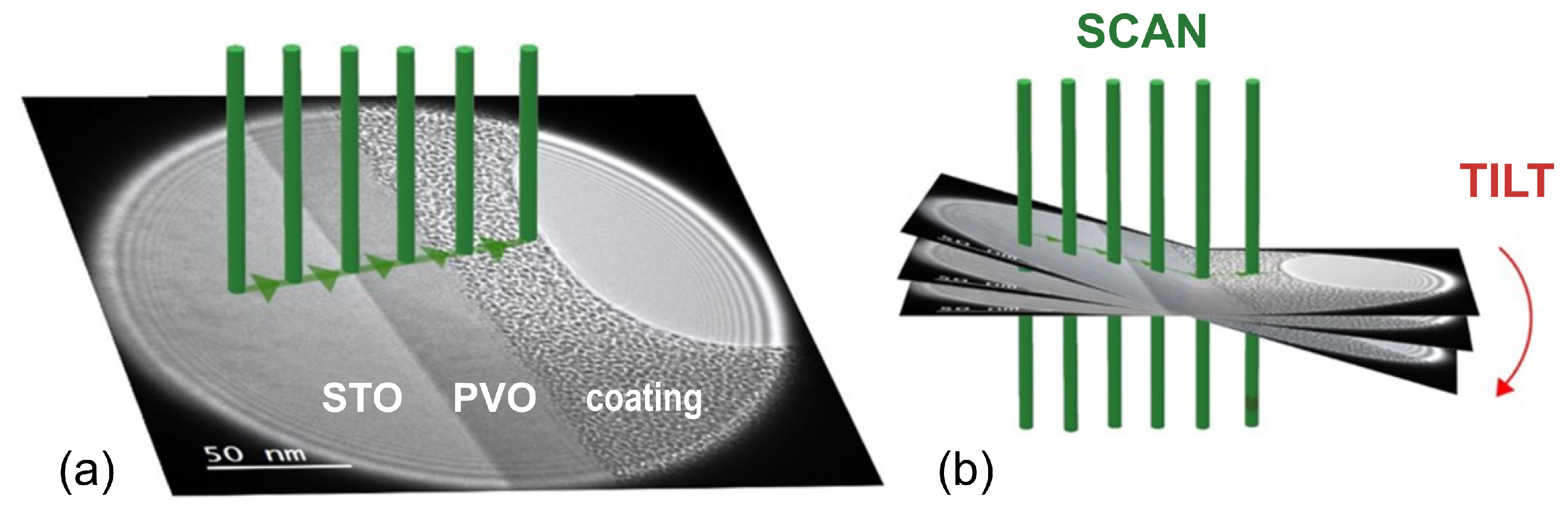
For thin films well below 100 nm thickness, the ability to collect PEDT data with smaller electron beams is key to access relevant structural information. With advances in transmission electron microscopy (TEM) functionalities, PEDT analysis using a 10 nm (or smaller) electron beam is now possible. This is paving the way for accurate full-thickness film analysis. Tracking issues will then be a major issue when using such small beams. An efficient way to perform such an analysis is to scan the electron beam across the thickness of the film, i.e., in a direction perpendicular to its surface, at each tilt angle during a PEDT acquisition (
Figure 1). Eggeman et al. [
9] actually exploited a similar approach for analyzing the domain volume and orientation in crystalline Ni-based superalloys and used the acronym SPET for scanning precession electron tomography data acquisition. This concept was also recently used by Rauch et al. [
10] in order to reconstruct in 3D the different domains composing a sample using parallel beam illumination. A related technique, namely 4D-STEM, consisting of acquiring 2D diffraction patterns on a 2D grid of positions, is already in use for performing orientation mapping with convergent beam illumination on multidomain samples composed of known phases [
11]. In these above-mentioned works, SPET or 4D-STEM are used for microstructure analysis and, essentially, map known crystalline phases and orientations over an area (2D) or, less often, on a volume (3D).
In this study, we present preliminary results aimed at testing the potential of SPET for structure analysis and the outcomes of our investigation utilizing a 10 nm electron beam that traverses a 35 nm
(PVO) thin film deposited on a
(STO) substrate. With a single SPET acquisition, we were able to analyze several ROIs throughout the thickness of the sample, achieve an ab initio structure solution and obtain accurate unit cell parameters and atomic coordinates for each one of the ROIs through dynamical refinements. As a result, we could observe small structural variations along the film thickness with enhanced spatial resolution compared to our prior works [
8].
2. Materials and Methods
The object of our investigation is an epitaxial PVO[010]o thin film grown on STO[110]c substrate synthesized using pulsed-laser deposition as described in Kumar et al. [
12], and analyzed in the form of TEM lamella. At room temperature, PVO has an orthorhombic crystal structure characterized by the space group
(SG: 62) and unit cell parameters a = 5.4856 Å, b = 5.5606 Å and c = 7.7771 Å. On the other hand, STO adopts a perovskite cubic structure with space group
(SG: 221), and its unit cell parameter is a = 3.905 Å. TEM imaging observations made on the same cross-sectional lamella utilized in this study and our prior work [
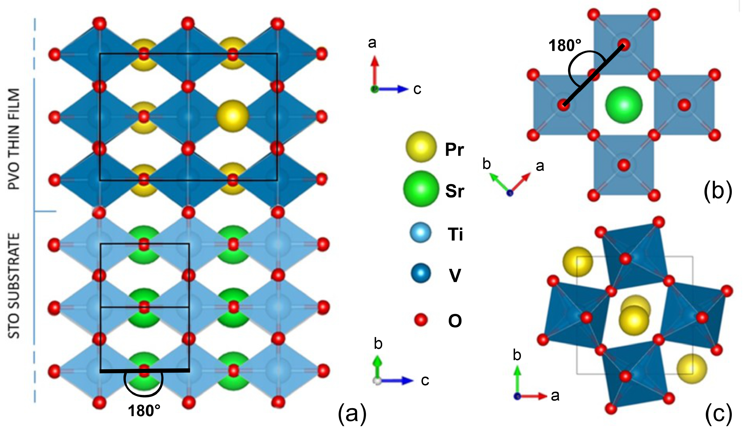
12] confirmed that the film is similar to a single domain throughout its length and thickness. This is rather uncommon for epitaxial oxide thin films, where domains with different orientations are frequently present. However, we considered that this characteristic could serve as a model thin film system for testing the ability of SPET to access structural information over a sample area and, in the present case, the thickness of the film. Given that the bulk STO exhibits an
tilting system in accordance with Glazer’s notation [
13], while bulk PVO has an
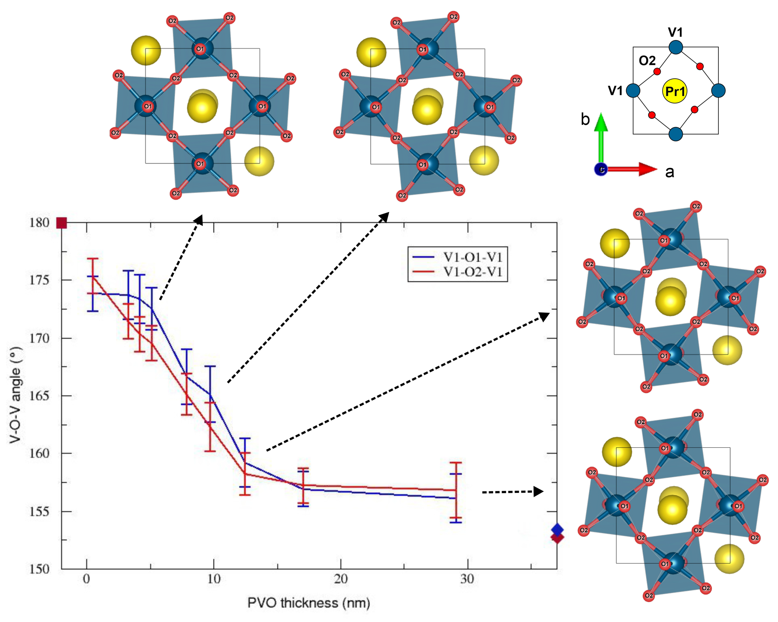
tilt pattern, we anticipated observing a completely strained segment of the film close to the substrate, as depicted in
Figure 2a. This implies, for instance, that the V-O-V angles of PVO would be close to 180°, as is the case in the perovskite structure of STO (
Figure 2b). As we moved away from the substrate, we expected a relaxation of the strain imposed on PVO. Eventually, it returned to a configuration of the atoms close to the one observed in bulk PVO, including octahedral tilt amplitudes (
Figure 2c).
SPET produces a series of PEDT data recorded at once on different ROIs. They were acquired using a JEOL F200 (200 kV) TEM equipped with a NanoMEGAS Digistar unit capable of generating simultaneous precession and line scan motions. A 10 nm diameter electron beam was scanned in a direction perpendicular to the interfaces, from the substrate to the coating with a step of approximately 0.92 nm between two acquisitions, resulting in oversampling of the same area of the film. The diffraction patterns were acquired with an ASI Cheetah M3 hybrid pixel detector (512 × 512 pixels) with 0.02 s exposure time. The precession semi-angle was set to 1.4
. A goniometer tilt step of 2
was applied after each line scan in the range [+44
,
], while a tilt step of 1
was used in the range [
,
]. To avoid shadowing of the film by the substrate or coating during sample rotation [
8], the tilt axis was aligned with the direction of scanning. Importantly, no tracking of a specific area was performed between each goniometer tilt. A rapid visual examination was carried out to ensure that, for each tilt angle, the SPET data were systematically collected from the substrate to the coating.
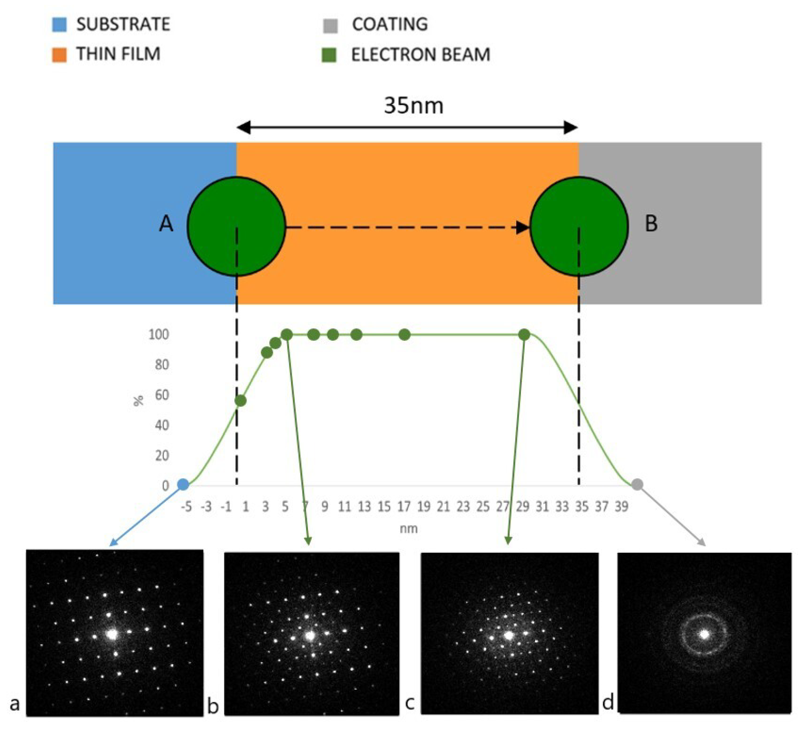
For analysis, PEDT data from one given ROI were extracted from the SPET series and processed using the program PETS 2.0 [
14]. In this work, only 9 ROIs (out of 38 collected) were selected for data processing as indicated in
Table 1 and in
Figure 3. As structural parameters change rapidly close to the substrate, more ROIs were taken into account in this part of the film. Each ROI is referred to in relation to the distance (in nm) from the substrate interface as presented
Figure 3. Collecting PEDT data from both the substrate and coating during SPET data collection serves two purposes. Firstly, it indicates when the film is entered and exited during the scan. Secondly, PEDT data obtained from the substrate can act as an internal standard, enabling an accurate determination of the unit cell parameters. This is achievable thanks to new functionalities recently implemented in PETS 2.0 to correct distortions induced by the microscope’s optical system and by the precession motion [
15]. To ensure a standardized procedure for data analysis, we first determined calibration constant and distortion parameters on STO and used them for the subsequent analysis of PEDT data collected on different ROIs of the film through its thickness. Kinematical and dynamical refinements were performed on JANA2020 with the results of the dynamical refinements reported in
Table 1. Note that while the kinematically derived R(obs) values typically fell within the range of 25 to 30%, the use of dynamical refinements resulted in a significant reduction in these values (
Table 1), accompanied by an enhancement in the accuracy of structural parameters.
We performed
first-principles simulations to corroborate the experimental lattice parameters and tilt angles obtained by SPET. For this, we used Density Functional Theory simulations using the Vienna Ab initio Simulation Package [
16] in combination with the meta-Generalized Gradient Approximation (meta-GGA) Strongly Constrained and Appropriately Normalized (SCAN) exchange–correlation functional [
17]. This functional was previously shown to produce the correct description in terms of the insulating or metallic character and structural parameters of various
transition metal oxide perovskites [
18]. Projector-Augmented Wave (PAW) [
19] potentials are used to model the core electrons and only the valence electrons are treated explicitly in the simulations—Pr 4
f electrons are included in the potential. The initial structure supplied to the solver is a
cell, corresponding to a 4 f.u supercell with respect to the primitive high symmetry
cubic cell and characterized by an
octahedral rotation pattern in Glazer’s notation [
20]. It is accompanied by an AFMC order consisting of AFM couplings between nearest V spins in the
-plane and a FM coupling between consecutive planes along the
c axis. This magnetic order is observed experimentally at low temperatures [
21]. The structural relaxation is performed until forces acting on each atom are lower than 0.005 eV/Å. The epitaxial strain experienced by the film is finally modeled by imposing two lattice parameters of the PVO
cell to that of a (110)-oriented STO substrate and the third one is free to relax in amplitude and direction.
3. Results
The first outcome is the ability to ascertain the epitaxial relationship by examining the 3D reconstructed reciprocal lattice from both the STO substrate and the PVO film. Using this direct output from 3D ED analysis, we confirm that the PVO film grows in the
b direction (
orthorhombic cell), with the
a and
c directions lying on the interface with the STO substrate. As a result, we anticipate that the lattice parameters in the
a and
c directions of PVO will be significantly constrained, while the lattice parameter in the
b direction may exhibit slight variations with respect to film thickness. However, determining the evolution of the lattice parameters as a function of film thickness using PEDT data remains a challenge. In our previous studies on thin films, this aspect was unaddressed due to the inherent limitations in determining the accuracy of lattice parameters. Thanks to the extensive efforts by P. Brazda et al. [
15], this limitation has recently been overcome, enabling us to apply this to thin films, which serves as a valuable test case.
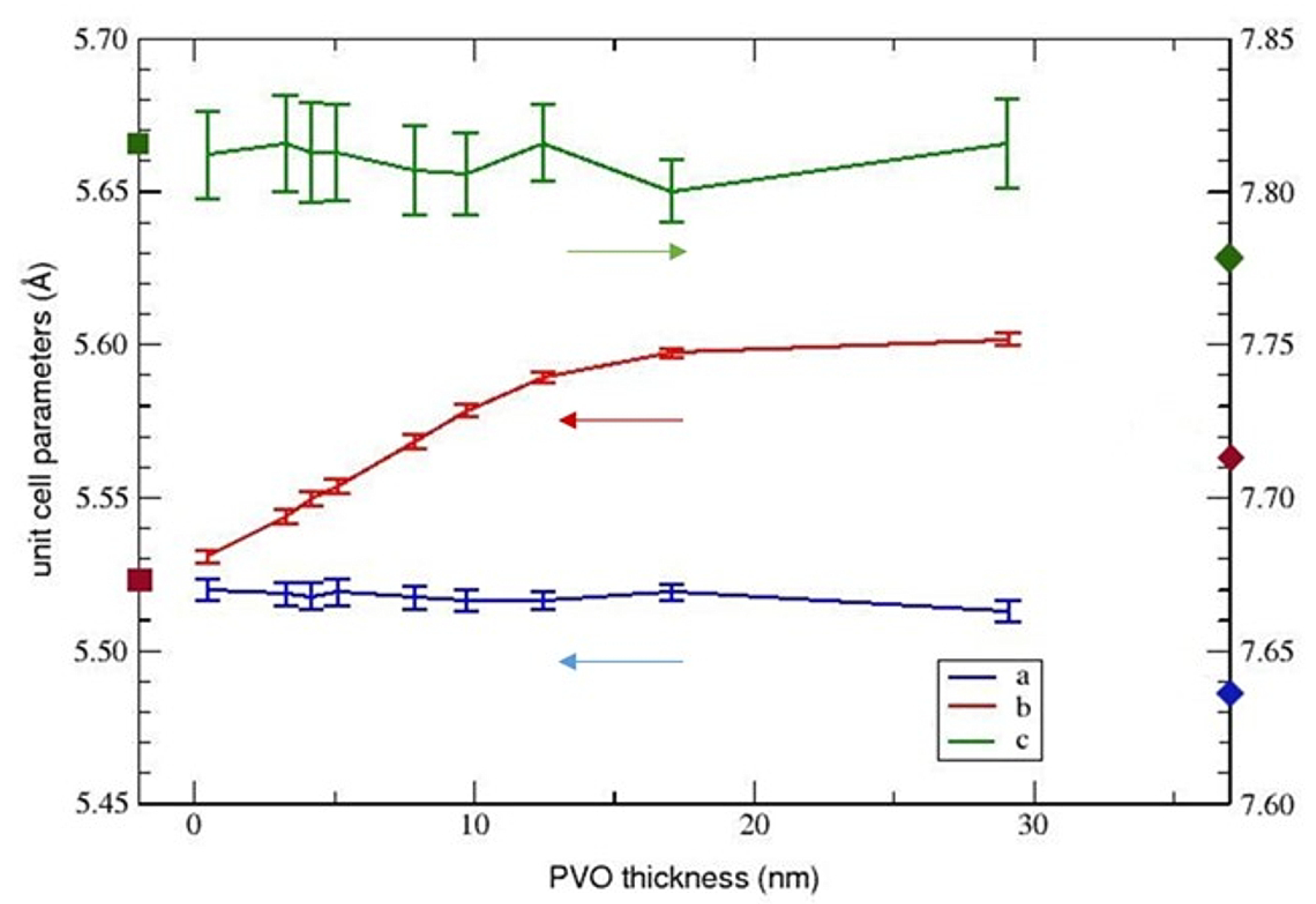
In
Figure 4, the unit cell parameters of the PVO film, obtained from the analysis of SPET data, are presented for various thicknesses of the sample. As mentioned in the section Materials and Methods, STO was used as an internal standard for determining the calibration and distortion parameters. Doing so, and without any other constraint imposed during the data processing, we first notice that the
a and
c parameters of the PVO film exhibit no significant variation along the film thickness, in agreement with the fact that they are strained to match the unit cell of the substrate throughout the thickness, as supported by the Reciprocal Space Mapping (RSM) published in Kumar et al. [
12]. At the interface with STO, there is no VO
6 octahedra rotation in PVO and the a and b parameters are expected to be equal, as observed. When we move away from the substrate, the structure of the film tends to return to a state close to the one adopted in the bulk material. The
b parameter is the only one not directly strained by the substrate and shows a notable increase, well above the standard uncertainty range, reaching a plateau after 15 nm. This indicates that the out-of-plane parameter relaxes with increasing thickness in order to accommodate some structural changes within the PVO film. Globally, the obtained lattice parameters at the free surface of the film (
Figure 4) do not match the ones observed for bulk PVO due to (i) the strain imposed by STO for a and c lattice parameters across the whole film and (ii) the progressive relaxation of octahedral rotations across the PVO film that produces an increase in the
b lattice parameter, as we will show later.
While not being the primary objective of this study, it is noteworthy to mention that the PVO structure can be determined
from the experimental intensities recorded using SPET. To know if the evolution of the lattice parameters as a function of the film thickness can actually be correlated to an evolution of the PVO structure, we performed dynamical refinements for different ROIs along the film thickness. Our focus was on two key structural features: the positioning of praseodymium within the perovskite cage and the rotation of the VO
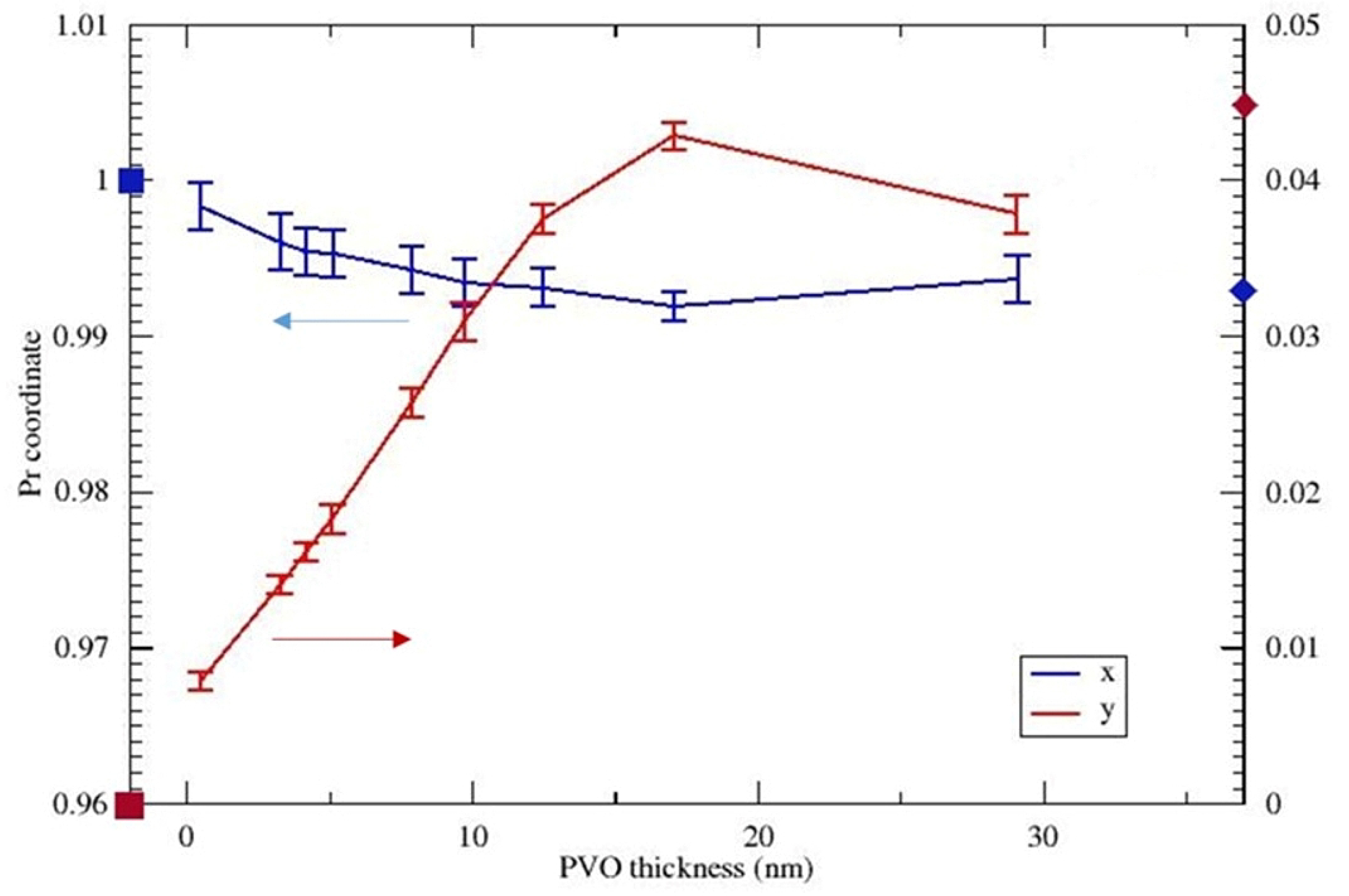
6 octahedra. Regarding the position of Pr in the unit cell, as represented in
Figure 5, only the x and y coordinates are considered since z is fixed by symmetry in the space group
. At the interface with STO, Pr is assumed to be in the center of the perovskite cage like Sr in STO with, here, coordinates x = 1 and y = 0 (square marks on the left
y axis
Figure 5). Looking at the Pr coordinates in bulk PVO (rhombuses marked on the right
y axis
Figure 5), the main difference is the y coordinate. Accordingly, while the x coordinate shows little variation across the film thickness, the y coordinate increases significantly to reach the bulk value. This variation is consistent with the strain relaxation along the film thickness observed for the
b parameter. Similarly, the evolution is strong between 0 and 15 nm and small after 15 nm. The evolution of the V-O-V angles, as plotted in
Figure 6, allows us to estimate the amplitude of the octahedral tilting across the film thickness. Close to STO, the substrate imposes a force onto the PVO structure so that V-O-V angles tend to be close to 180° (no rotation). Going away from the substrate, both the V-O1-V and V-O2-V angles show a decrease, i.e., an increment in the octahedral tilting amplitudes, up to 15 nm where a plateau is reached at about 156°, close to the values found in the bulk PVO structure.
The evolution of the lattice parameters and structural features obtained using SPET are, globally, consistent with what we could expect considering the strain relaxation where the film tries to recover a structure close to bulk PVO. If we look critically at these results, there are a few points that deserve attention. The first one is for the results obtained close to the interface with STO. As depicted in
Figure 3, using a 10 nm beam, no information can be obtained directly for the very first deposited layers of PVO as the diffraction signal is largely dominated by the substrate contribution. Only an interpolation can be made between a nontilted perovskite at thickness 0 and the PEDT data we obtained for thicknesses above 5 nm, for which the beam is entirely in the film. The second point is how to interpret the results after 5 nm, where we can state that the obtained structural difference with respect to the PVO bulk structure is not to be traced back to a contribution of the STO substrate in the diffraction patterns.
In order to obtain insight into the reliability of the SPET method for extracting structural parameters across the thickness of thin films, DFT simulations were performed on a [010]-oriented PVO film with respect to the orthorhombic cell. After the structural relaxation performed at 0 K, we observe that two lattice parameters are elongated with respect to the 0K DFT bulk structure (i.e.,
= 5.5225 Å and
= 7.8100 Å versus
= 5.4856 Å and
= 7.7771 Å), in agreement with the experimental measurement presented in
Figure 4. This leads to a small contraction of the
b lattice parameter in order to minimize the relative volume variation with respect to the bulk (
= 5.5230 Å versus
= 5.5606 Å). At first glance, this result disagrees with the experimental value at 293 K reported in
Figure 4 (i.e.,
b = 5.56 Å). Nevertheless, this discrepancy may originate from the fact that our DFT simulations are performed at 0 K and a fair agreement is indeed recovered once using the experimental
b parameter obtained at 5 K (
b = 5.6061 Å [
22]). Regarding the octahedral rotation amplitude, we extracted V-O1-V and V-O2-V angles of 152.3° and 154.1°, respectively. This indicates a slight reduction in octahedral rotation with respect to the DFT relaxed bulk in which the two angles are 151.4° and 153.0°. This trend agrees with the experimental observation for these two angles far away from the interface, where no substrate effect may be experienced by PVO (
Figure 6).
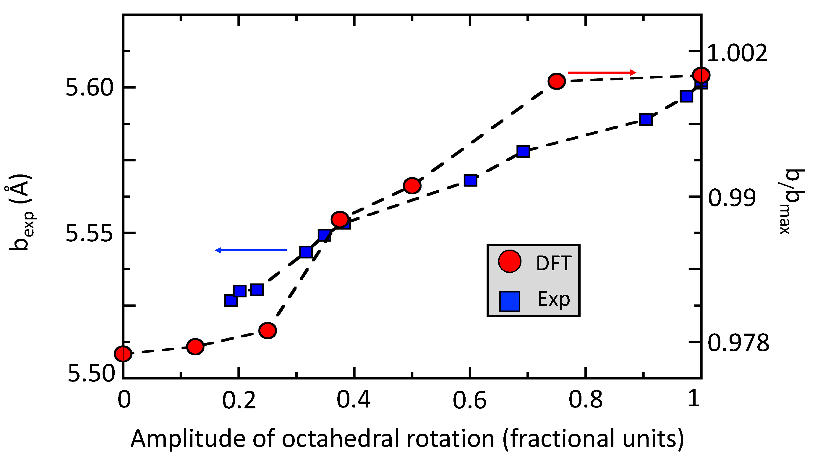
One can actually relate the evolution of the
b lattice parameter to the V-O-V angles (
Figure 7). Remarkably, we notice an elongation of the
b lattice parameter upon increasing the octahedral rotation amplitude. This behavior can be tracked theoretically by (i) fixing a fractional amplitude of the relaxed atomic positions with respect to the high symmetry cell from 0 (no distortion) to 1 (total distortion appearing in the strained material) and (ii) performing relaxation of the
b lattice parameter. The evolution of b/b
max with the octahedral rotation amplitude from DFT is reported in
Figure 7. We observe that without any octahedral rotation, the
b lattice parameter is expected to be rather small. From 0.25 to 0.75, a progressive elongation of
b is observed. Above 0.75,
b reaches a plateau with its maximal elongation. The overall trend of
b versus the octahedral rotation amplitude is well reproduced by DFT, confirming the reliability of the experimental measurements.
4. Conclusions
In this work, we introduced a new approach to thin film characterization based on 3D ED. SPET has been previously used [
9,
10] to obtain crystallographic phase and orientation mapping on a volume. In this study, we extracted electron diffraction intensities (3D ED datasets) from different ROIs and analyzed them quantitatively, aiming for accurate structure refinements. Specifically, SPET was used on a 35 nm PVO thin film, combining a scanning procedure with PEDT. By scanning with a nanobeam of 10 nm diameter along the PVO film thickness at every tilt step during a PEDT experiment, we could analyze the film structure at different thicknesses by properly sorting the acquired diffraction patterns.
Cell parameters and atomic positions were accurately determined and an evolution along the thickness of the film was observed in the out-of-plane unit cell parameter, as well as in the tilting of the VO6 octahedra and in the y coordinate of the Pr atoms. These variations are coherent with the expected constraint given by the substrate in the first layers, and afterwards with the expected gradual relaxation of the crystal structure. At the interface with STO, oxygen atoms in PVO are pinned by the substrate and the angles are close to 180°, causing the smallest value of the b parameter. Progressively moving farther away from the interface, V-O-V angles go towards smaller values and then b increases. Finally, far away from the interface, the V-O-V angles exhibit their smallest values and hence b reaches its largest amplitude and a plateau. By comparing the experimental results and DFT calculations, we demonstrated that SPET in nanobeam configuration is a valid technique to obtain accurate information about subtle changes in the crystal structure of thin films. These results obtained by a 3D ED method at such a small scale are pioneering.
Since these variations are known to occur in the first few nm of thin films, also depending on the degree of constraint given by the substrate, it is fundamental to use, for such experiments, an electron beam diameter as small as possible in order for the results of the refinement to be as accurate as possible with respect to each probed region of the sample. Implementing the data acquisition strategy and improving the diffraction pattern sorting procedure, this analysis has the potential to become faster and even more accurate, paving the way for a new routine characterization for thin films. This can in turn lead to an important step forward in the field of thin film engineering, finally making it possible to link their physical properties to their accurately determined crystal structure.


