1. Introduction
Electrification is an essential part of the development of society and is important in many environments, including industry, transportation, security, household, and others. Its application leads to a significant reduction in the use of fossil fuels as sources of energy, thereby ensuring the ecological balance in nature. This determines electrification as one of the most important and priority tasks of the most developed countries and economic unions. In this sense, power electronics are the main tool for the practical implementation of electrification, and DC/AC converters are one of the main groups of power electronic devices [
1]. They are used as sources of high-frequency electricity for a variety of needs: industrial and household applications, wireless power transmission, high-efficiency lighting, for efficient energy storage and distribution, and others [
2].
Resonant converters represent a significant part of DC/AC converters [
3]. They have a number of advantages, the most important of which are [
4]: implementation of work with “soft” commutations; well regulation characteristics; possibility of operation in modes close to short circuit under load conditions; and use of parasitic circuit elements as part of the resonant circuit. In this way, they are characterized by high energy, mass, size and economic indicators, etc. [
5].
The commercialization of resonant converters and scientific research in this area in the last 50–60 years were conditioned by the emergency, development, and great variety of various industrial technologies such as: induction heating [
6], brazing [
7], melting, alloying, soldering, welding [
8], and in recent years for the preparation of nanostructures and nanomaterials based on electromagnetic stirring [
9].
For some time, there was a trend of using and transferring knowledge and experience from industrial technologies in systems for contactless transmission of electrical energy, as well as in the home: induction stoves and cooktops [
10,
11], induction boilers and heaters [
12], implementation of high-efficiency lighting fixtures, etc. [
13].
Another important factor that contributed to the rapid development of topologies and technologies for the analysis, design, prototyping, and operation of DC/AC converters is the growing energy needs due to the increase in the living standards of the Earth’s population [
14]. This necessitated the use of DC/AC converters in other fields of technology as well: decentralized electricity generation from renewable and alternative sources [
15], electric transport [
16], charging stations for electric cars [
17], in “smart” power grids, etc. [
18].
Additionally, the diverse topologies, the different types of power semiconductor elements, make it possible to implement a very large set of control algorithms and, accordingly, operating modes. In this aspect, there are numerous studies dedicated to the analysis, design, and prototyping of a specific power electronic device, taking into account the specifics of its application. Static characteristics of resonant converters operating in resonance modes are presented in [
19]. They were obtained by analyzing idealized series resonant circuit converters under various combinations of connected voltage sources. The proposed procedure allows for obtaining expressions for calculating the steady-state current of the AC circuit. In [
20], a high-power resonant converter applied to power an induction furnace for steel melting is shown. To reduce switching losses, zero voltage switching (ZVS) is achieved in the H-bridge converter. In [
21], a new high-accuracy simulation design tool for DC-DC resonant converters is proposed. The design tool uses generalized time domain analysis applicable to multiple resonant converter configurations. A performance analysis of a new resonant converter circuit configuration using a sinusoidal approximation is shown in [
22]. A 250 W prototype of the proposed resonant converter was built to validate the analysis proposed in this paper and evaluate its performance. In [
23], the analysis and design of a current source fed a parallel resonant (CFPP-PR) converter for cooker magnetrons is given. To demonstrate the analysis and design, a resonant converter was built and tested. The simulation and experiment results match those obtained from the analysis. Fundamental frequency analysis was used to analyze the steady-state operation of the three most popular resonant DC/AC converters: series, parallel-compensated load, and series-parallel [
24]. Transfer characteristics are presented, which were obtained by describing the resonant nature of the principle of operation of the power circuit. These characteristics are valid for operation with a limited frequency range (close to the resonant frequency of the AC circuit) and enable the determination of circuit elements. The validity of the proposed design ratios and the identified optimal operating conditions are confirmed by time domain simulations and measurements on a series-parallel resonant converter prototype. Another way to analyze and design resonant converters containing a large number of reactive elements is model reduction [
25]. It is known that the complex equivalent circuit (of high order) in the small-signal modeling of the resonant converter is a barrier to the derivation of analytical dependencies and the physical interpretation of the processes in the power circuit. This paper presents the analysis and design of a series resonant converter (SRC) based on AC circuit order reduction by approximation. The strong influence of the loops that contain the resonant inductance and the resonant capacitor on the accuracy of the approximation is investigated. In this aspect, a reduced third-order equivalent circuit of the device is proposed. When operating in modes with the control frequency close to the resonant frequency, a negligible difference is observed between the reduced and the full model of the DC/AC converter. The validity of the proposed equivalent scheme is confirmed by the results of the simulation.
From the analysis of numerous publications on this topic, it follows that there is a lack of up-to-date research that addresses the methodological aspect in the study of power electronic devices and systems and where engineering design methodologies are presented and discussed.
The aim of the present work is to demonstrate an innovative methodology for the design consideration of a whole class of power electronic devices—resonant DC/AC converters. In this sense, the main tool for achieving this goal is the unified approach presented by the author for the analysis of DC/AC converters, based on the study of processes in a series RLC circuit [
26]. The manuscript is organized as follows: the first chapter describes the basic concepts and applications of resonant DC/AC converters. Various analysis and design approaches are considered. The second chapter is devoted to the methodological basis of the unified approach for the design of resonant DC/AC converters. In the third chapter, transmission functions of resonant DC/AC converters with and without reverse diodes operating in modes with soft and hard commutation of the semiconductor bars are determined. In the fourth chapter, the most frequently applied complicated output circuits are analyzed, through which the agreement between the parameters of the inverter and the load is carried out. In the fifth chapter, the unified methodologies for the design of parallel and series resonant DC/AC converters with and without reverse diodes are presented. In the sixth chapter, calculation examples are presented, through which the unified design methodologies were verified.
Section 6 provides discussion and conclusion.
The motivation for conducting this research is related to the fact that there is currently a lack of up-to-date publications related to theoretical summaries and considerations. They are very useful both from a methodological point of view for designing specific types of power electronic devices and for training in power electronics. In this sense, the main idea is to present the developed innovative and rational methodologies, allowing for formalization and automation of the design process.
2. Methodological Basis of the Innovative Design Approach
Regardless of the great variety of applications of DC/AC converters, from the point of view of electrical engineering, their equivalent AC circuits are presented most often with a series substitution scheme. For example, in electrical technologies, a substitution circuit consisting of an active load
R and a reactive load
ωL is used. In this case, the loads for the DC/AC converters are active inductive with a very low power factor
cosφT [
27,
28,
29,
30]. On the other hand, due to the requirement to obtain a certain active power, it is necessary to compensate the loads with capacitors. Depending on the way the capacitors are connected to the load, parallel and series compensation and a series or parallel load resonant circuits are obtained [
27,
30].
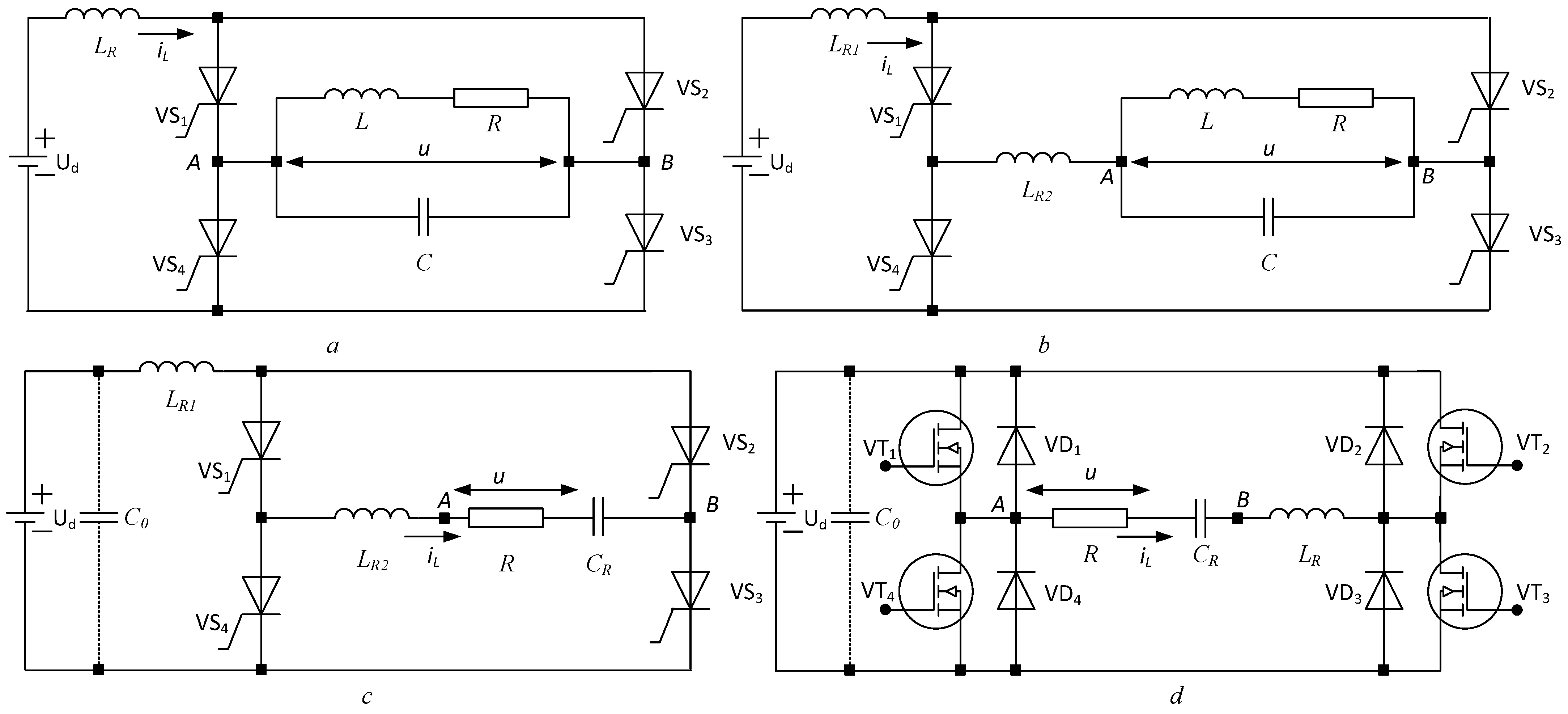
Figure 1 shows basic schemes of resonant DC/AC converters, using parallel (
Figure 1a,b) and series compensation (
Figure 1c,d).
Due to the properties of semiconductor elements, thyristor circuits (
Figure 1a–c) are without reverse diodes, while transistor circuits (
Figure 1d) are with reverse diodes. On the other hand, in circuits without reverse diodes when operating in soft switching mode (zero-current switching), it is possible to divide the resonant inductance into two parts (
Figure 1b,c), which achieves different levels of voltage loading on the thyristors [
29].
Due to the specificity of the load, the quality factor of the parallel resonant load circuit has typical values in the range
Q = 3 ÷ 30. In this case, the load circuit acts as a filter for the higher current harmonics in the AC circuit of the inverter. In this way, the influence of all current harmonics in the AC circuit without the first can be neglected on the load [
28,
30]. Then, for analysis and design purposes, the parallel resonant load circuit is replaced by series-connected active
R(1) and reactive
X(1) impedance components at the first harmonic of the current in the AC circuit. These ingredients are defined by the expressions [
30]:
where
Re is the active resistance from the parallel replacement circuit of the series
RL load and
γ is the angle between the current in the inverter AC circuit and the load voltage.
In a number of cases, the series compensation is also used, where a compensating capacitor is connected in series with the active-inductive load. This type of compensation is of practical importance when working with inductors with higher values of
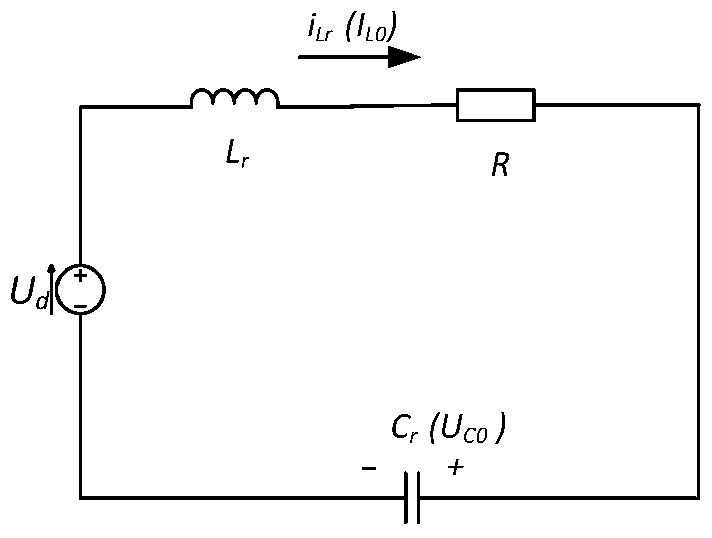
cosφT of the load. In industrial technologies, the loads are low-impedance, and thus the series compensation in a natural way results in a series resonant circuit. In this sense, regardless of the type of compensation, the AC circuit of the resonant inverter, which can be of arbitrary complexity, is represented equivalently, by the first harmonic of the control frequency, with a series RLC circuit. The generalized serial equivalent circuit corresponding to these considerations is shown in
Figure 2.
In this context, the following values of the elements of the generalized serial equivalent scheme are valid for the various circuit variants:
In series compensation, R is the active component of the load, CR is the resonant capacitor, and the resonant inductance LR can be composed entirely of the inductive component of the load L or added as an additional inductance to the resonant one—LK;
In parallel compensation, the active resistance in the circuit R = R(1) is the equivalent active resistance at the first harmonic of the control frequency of the parallel load circuit, the resonant capacitor CR = C(1) is the equivalent reactance at the first harmonic of the control frequency of the parallel load circuit, and the resonant inductance LR can be entirely in the inverter DC circuit, entirely in the inverter AC circuit, or divided in any ratio between them.
When using complex resonant output circuits to match the parameters of the inverter and the load, again the equivalent circuit of
Figure 2 is valid, but the relevant parameters of the series RLC circuit are determined by a more complicated procedure, which is described in the following sections of the manuscript. On the other hand, in some of the schematic varieties of resonant DC/AC converters, the roles of resonant elements can also be performed by the detuned parallel resonant load circuit when a parallel compensated load is used.
For the description of the principle of operation of the power circuit, the unified approach for the analysis of DC/AC converters presented in [
26] is applied. In this aspect, the coefficients introduced in the unified analysis were used in the design of this class of power electronic devices:
- -
coefficient of variation ;
- -
detuning factor of the equivalent resonant circuit ,
where is the damping factor, is the resonant frequency of the equivalent series resonant circuit, and ω = 2f is the angular control frequency.
A conduction angle of the semiconductor switches
λ = πν, normalized to the control frequency, was also introduced, which allows a unified consideration of all operating modes. Another basic characteristic of the equivalent series resonant circuit is the angle
β between the current in the AC circuit and the output voltage of the inverter, which is defined as follows:
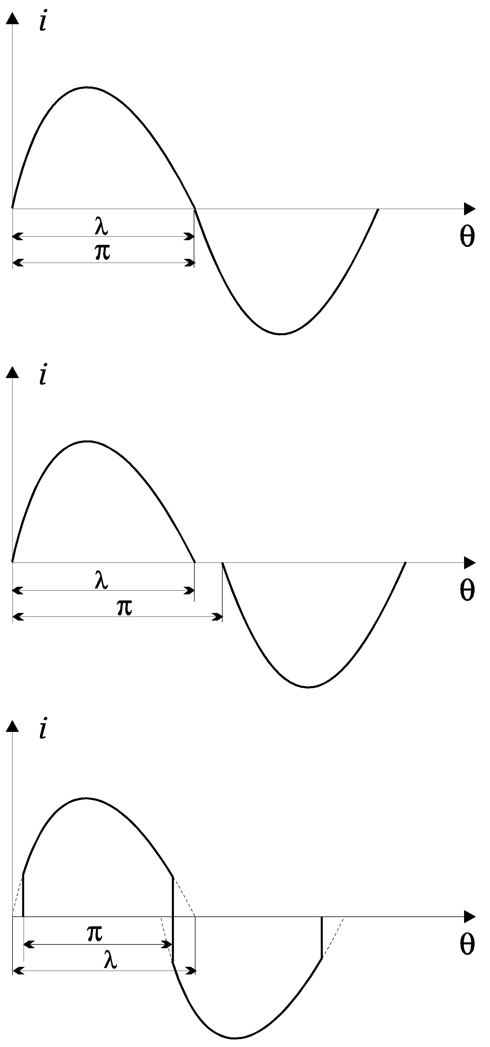
In resonant DC/AC converters without reverse diodes, depending on the ratios between the control frequency and the resonant frequency of the equivalent AC circuit, three modes of operation are possible, as shown in
Figure 3 [
29,
30]:
- -
border current mode when the driving frequency coincides with the natural frequency of the series resonant circuit ω0, i.e., λ = π;
- -
continuous–discontinuous current mode, also known as natural switching mode of the semiconductor components, in which ω < ω0, i.e., λ < π;
- -
continuous–continuous current mode, also known as a forced switching mode of the semiconductor components, when ω > ω0, i.e., λ > π.
From the point of view of switching semiconductor devices, these operating modes can be reduced to: soft switching mode that includes the border and continuous–discontinuous current mode and hard switch mode, which is relevant to the continuous–continuous current mode, also known as the current source inverter.
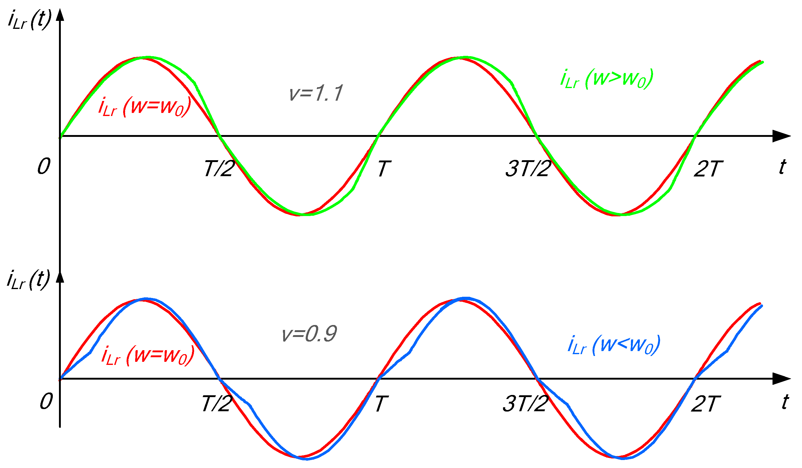
Resonant DC/AC converters with reverse diodes usually operate in continuous–continuous current mode, which is more energy efficient. In this sense, depending on the value of the detuning coefficient
ν, two main modes are observed with a control frequency below or above the resonance.
Figure 4 shows the shape of the current in the AC circuit in the two operating modes. In addition, the shape of the current when operating in the resonance mode is given as a reference, which gives an idea of the change in the shape of the current at different values of the detuning factor.
Usually, the analysis of the work of resonant DC/AC converters is carried out on the basis of full-bridge schemes, with the help of known numerical odds [
30], the results obtained can also be spread to other diagram varieties of resonant DC/AC converters (half-bridge, with a split resonance capacitor, with zero conclusion of the inverter transformer, etc.). Full (transistors) or semi-controlled (SCR) semiconductor devices may be used as switch elements.
In order for the operation of the resonant inverter to be possible, regardless of whether the devices are fully controllable (transistors) or half controllable (thyristors), it is necessary that the AC circuit of the inverter have a capacitive response (character), i.e., the current in the circuit be ahead of the output voltage of the inverter in phase. This can be expressed as follows [
29]:
where the coefficient
reflects the distribution of the individual parts of the resonant inductance between the input (DC) circuit and the output (AC) circuit of an inverter.
Using the expression for the resonant frequency of the equivalent series resonant circuit and after mathematical transformations, the following expression is obtained for the quantity
:
In this way, expression (3) is obtained in the form:
Since the unified analysis of DC/AC converters uses the coefficient of variation k, it is more convenient for design purposes to use:
Formula (6) gives the relationship between the values of the elements of the AC circuit of the resonant inverter and the coefficients k and ν, which give information about the mode of operation of resonant DC/AC converters.
4. Resonant DC/AC Converters with Complex Output Circuit
The unified approach to the analysis of resonant DC/AC converters operating in different modes, considered in the present work, allows these power electronic devices to be designed in direct connection to the load or by using a matching output transformer.
In cases where it is necessary to improve the load characteristics of resonant DC/AC converters and increase their energy indicators, resonant DC/AC converters with complicated output circuits are used. This necessitates the consideration of their impact on the AC circuit, and also for the optimal design of the elements of these circuits.
The most commonly used in practice complicated output circuits are resonant and are as follows [
30]:
- -
series-parallel output circuit;
- -
parallel-serial output circuit;
- -
series-parallel-parallel-serial output circuit.
4.1. Series-Parallel Resonant Output Circuit
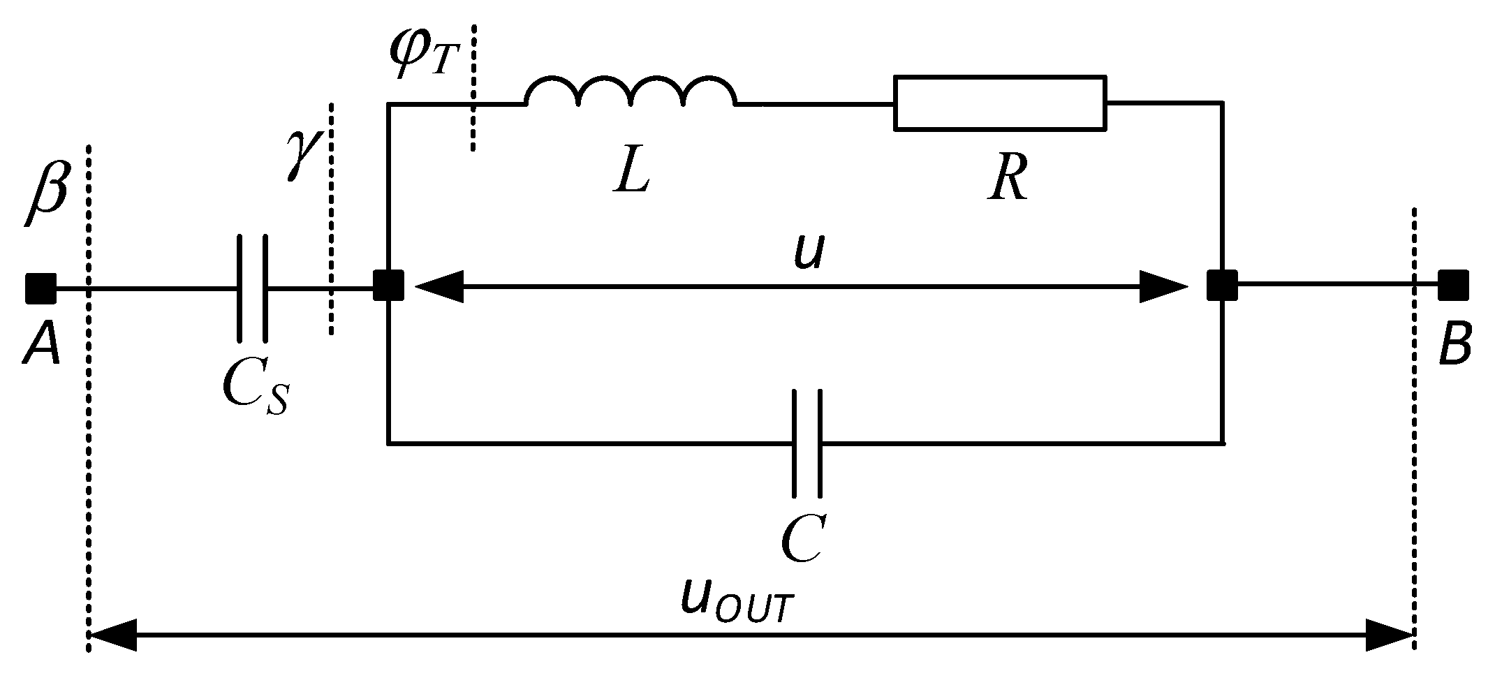
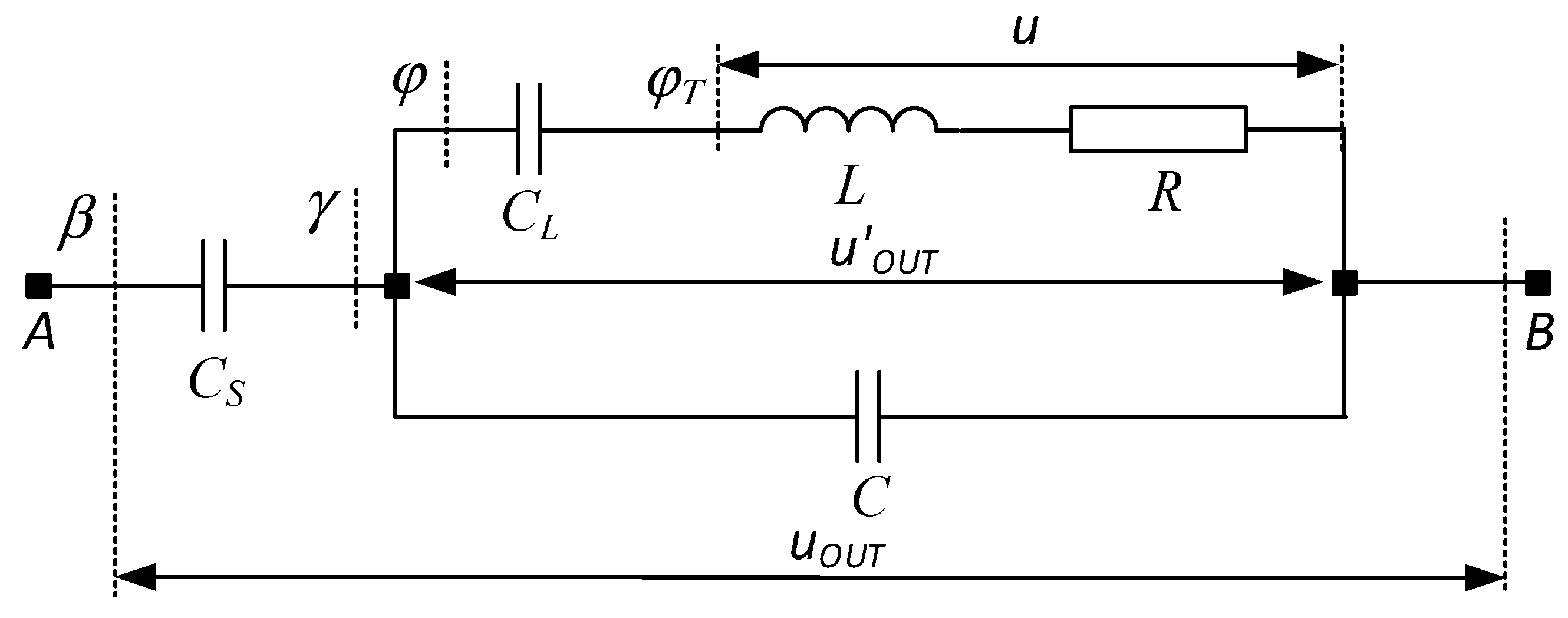
The schematic of a series-parallel resonant output circuit is shown in
Figure 6. To obtain a series-parallel resonant inverter circuit, it must be connected to each of the power circuits in
Figure 1 between the points labeled A and B. The following notations are used:
R and
L are the parameters from the load’s series substitution circuit,
CS—series capacitor, and
C—compensating capacitor connected in parallel with the load.
When determining the base ratios for the considered output circuit, the ratio of the load
U to the output voltage
UOUT expressed by the coefficient
is introduced. As parameters for the determination of the analytical dependences, the coefficients already introduced in the analysis of the DC/AC converters will be used: of oscillation
k, of detuning
ν, and the power factor of the load
cosφT. In order to obtain the relationship between the load voltage and the output voltage of the inverter, and also to apply any of the transfer function already determined, the circuit shown in
Figure 6 needs to be converted to obtain an equivalent series R-C load. Such transformations are presented in [
27], where the concepts of real and ideal detuning of the corresponding resonant circuits are used to express the parameters of the equivalent load. This leads to a significant complication of both the calculation procedures and the physical interpretation of the processes in the power circuit. Another approach is proposed here, which leads to significant simplifications in the determination of analytical dependences and also in the design of resonant DC/AC converters with a complex output circuit. The tool used to achieve this goal is impedance and conductance triangles. Plots that represent the conversion of the output circuit are shown in
Figure 7 [
28].
The components of the equivalent impedance of the parallel load circuit composed of
R,
L, and
C are described by the active resistance of the parallel substitution circuit of the RL load
Re and the angle between the current in the AC circuit and the load voltage
γ. Depending on the sign of
γ, the load circuit is either in capacitive or inductive fault, and in the case of resonance
γ = 0. In [
29,
30], it was proven that regardless of the mode of operation of the series-parallel resonant inverter (continuous–discontinuous or continuous–continuous current mode), the capacitive detuning of the load circuit is preferred. Therefore, this case is considered here and the corresponding constructions from
Figure 7 are made for it. The conversion of the series-parallel circuit takes place in the following sequence: first, the series load circuit
R,
L is converted into an equivalent parallel one with the corresponding elements
Re,
Le. During the conversion, the angle
φT between the load current
I and the load voltage
U is preserved; as a result of the capacitor
C included in parallel with the load, the load inductance is compensated and the load resonant circuit is equivalent to active resistance
Re and capacitive reactance
Xe; the circuit impedances thus obtained from the parallel substitution circuit are transformed into a series equivalent circuit with elements
RSER and
XSER, and in this transformation the angle
γ is preserved; the addition of the series capacitor
CS increases the detuning angle of the parallel load circuit
γ. Thus, in the equivalent substitution circuit, a dephasing angle
β is obtained between the current in the AC circuit and the output voltage
UOUT. As a result, the series-parallel output circuit is replaced by series-connected active component
RΣ and capacitive component
XΣ of the impedance.
From the balance of the active power at the output of the inverter is obtained [
30]:
As a result of the basic ratios obtained from the analysis of resonant DC/AC converters, angle β is determined by (3). In this aspect, to obtain the relationship between the output and the load voltage, it is necessary to find an analytical dependence for cosγ.
The determination of
γ was carried out on the basis of the geometric constructions shown in
Figure 7 and is carried out with:
where
.
Finally, considering some trigonometric transformations, it turns out that:
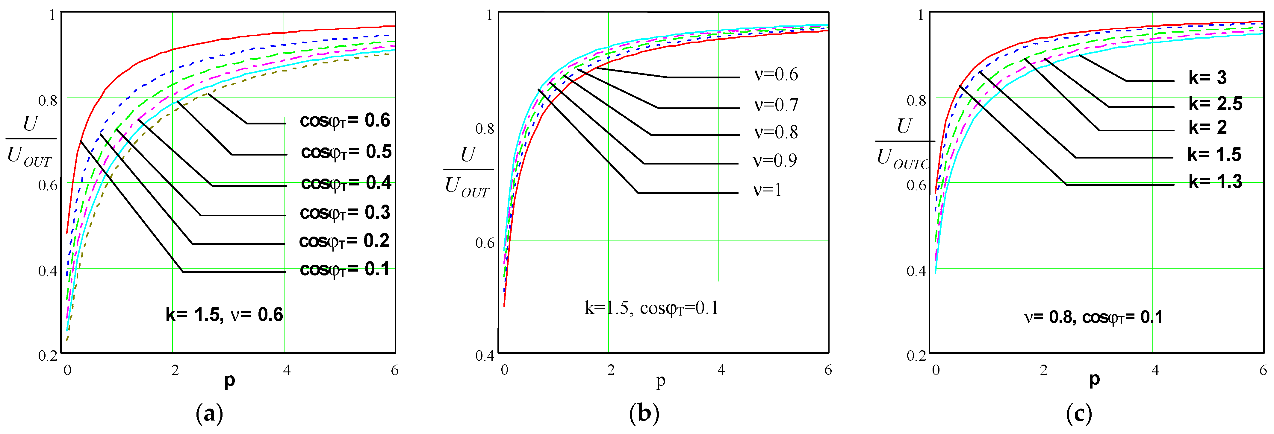
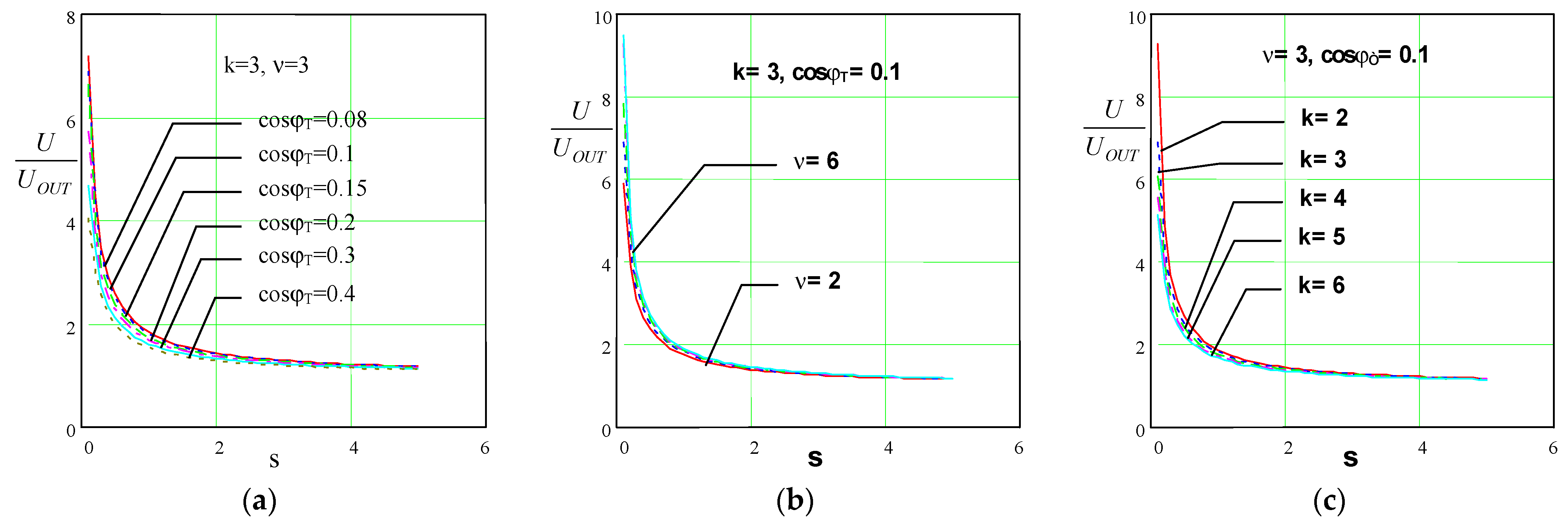
Figure 8 shows the dependence
, with parameters
k,
ν, and
cosφT, when operating a resonant inverter in soft commutation mode.
The following conclusions can be drawn from it:
As cosφT decreases, the ratio U/UOUT increases.
Increasing the detuning factor ν leads to an increase in the U/UOUT ratio.
An increase in the coefficient of variation k leads to a decrease in the ratio U/UOUT.
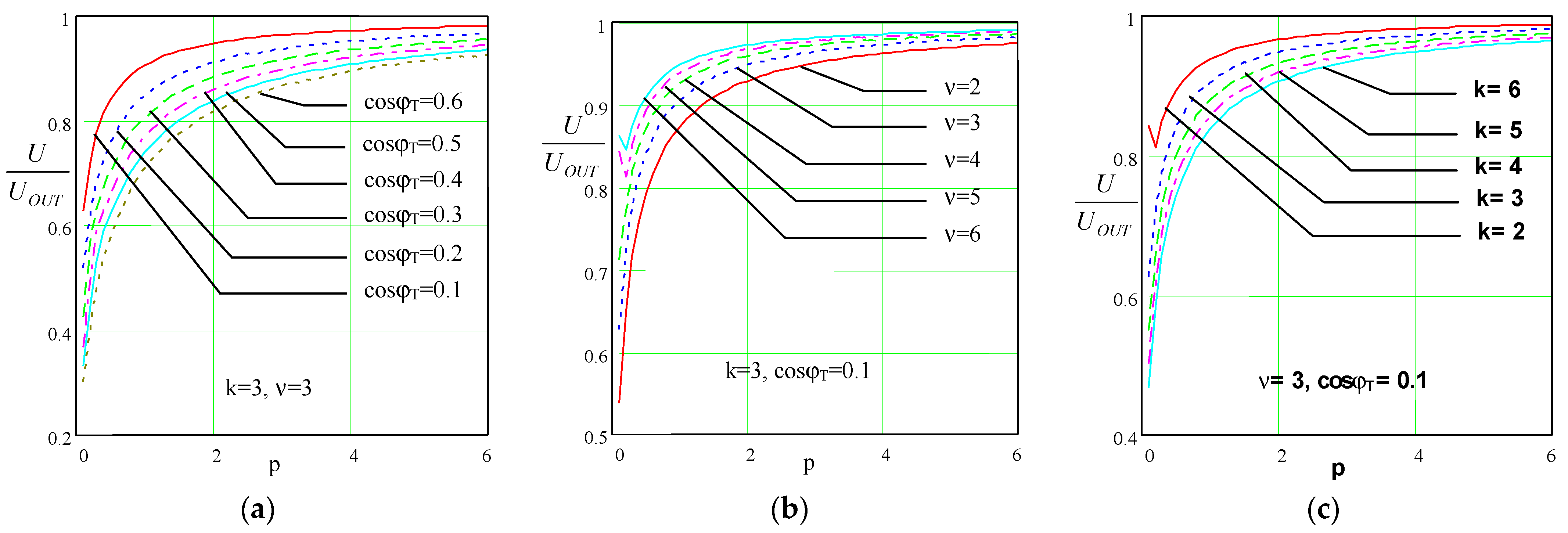
Figure 9 shows the dependence
, with parameters
k,
ν, and
cosφT, for the operation of a resonant inverter in hard commutation mode (current source inverter). The following conclusions can be drawn from its appearance:
As cosφT decreases, the ratio U/UOUT increases.
Increasing the detuning factor ν leads to an increase in the U/UOUT ratio.
An increase in the coefficient of variation k leads to a decrease in the ratio U/UOUT.
From the look of
Figure 8 and
Figure 9, it can be seen that an increase in the coefficient
p leads to an increase in the ratio
U/UOUT.
The constructed characteristics confirm the conclusions known from the literature that the series-parallel resonant output circuit with the operating mode chosen in this way should be used to match the inverter and a load that requires a lower voltage than the output.
4.2. Parallel-Series Resonant Output Circuit
The schematic of the parallel-series resonant output circuit is shown in
Figure 10. To obtain a parallel-series resonant inverter, it must be connected to each of the power circuits in
Figure 1 between the points labeled A and B. The following notations are used:
R and
L are the parameters from the series substitution circuit of the load,
CL—capacitor connected in series with the load, and
C—capacitor connected in parallel with the load. For the purposes of creating engineering methodologies for design, it is necessary to find an analytical expression of the function
, with parameters of this functional dependence as the coefficient of variation
k, the detuning factor
ν, and the load power factor
cosφT, where
.
Similarly to the previous case, the circuit shown in
Figure 10 is successively converted to obtain an equivalent complex R-C load, using the representation of the circuit elements by an impedance triangle shown in
Figure 11. The series resonant circuit composed of
R,
L, and
CL can operate in both inductive and capacitive tuning. In [
30], inductive detuning is justified as more favorable from the point of view of current and voltage loading of semiconductor switches, and it is for this case that the present considerations were made.
In the case of a parallel-series output circuit, the series load R and L is partially compensated (because this circuit is in inductive detuning) by the capacitor CL in series with the load. As a result, an equivalent series impedance with an active component R and an inductive component is obtained. This impedance is converted into an equivalent, but consisting of parallel connected active () and reactive () components of the admittance. Due to the equivalence requirement of the conversion from series to a parallel substitution circuit of the considered circuit, the angle φ between the load current I and the output voltage UOUT is preserved. The thus obtained active-inductive complex load is compensated with the parallel capacitor C and an equivalent impedance with an active component () and a capacitive component () is obtained. The triangle of conductances thus obtained is then converted into a triangle of resistances, as a result of which the parallel-series output circuit is replaced by a series-connected active RΣ and capacitive XΣ components of the impedance. Thus, in the equivalent substitution circuit, a dephasing angle β between the current in the AC circuit and the output voltage UOUT is used.
In [
30], it was shown that, due to the balance of active powers in the output circuit, we have the dependence:
Since cosφT for a given load is known in advance and is involved as a parameter in finding the characteristics of the parallel-series resonant inverter, it remains to determine cosφ.
The determination of
φ is carried out on the basis of the geometric constructions shown in
Figure 11 and is carried out with:
where
.
By using trigonometric transformations, it turns out that:
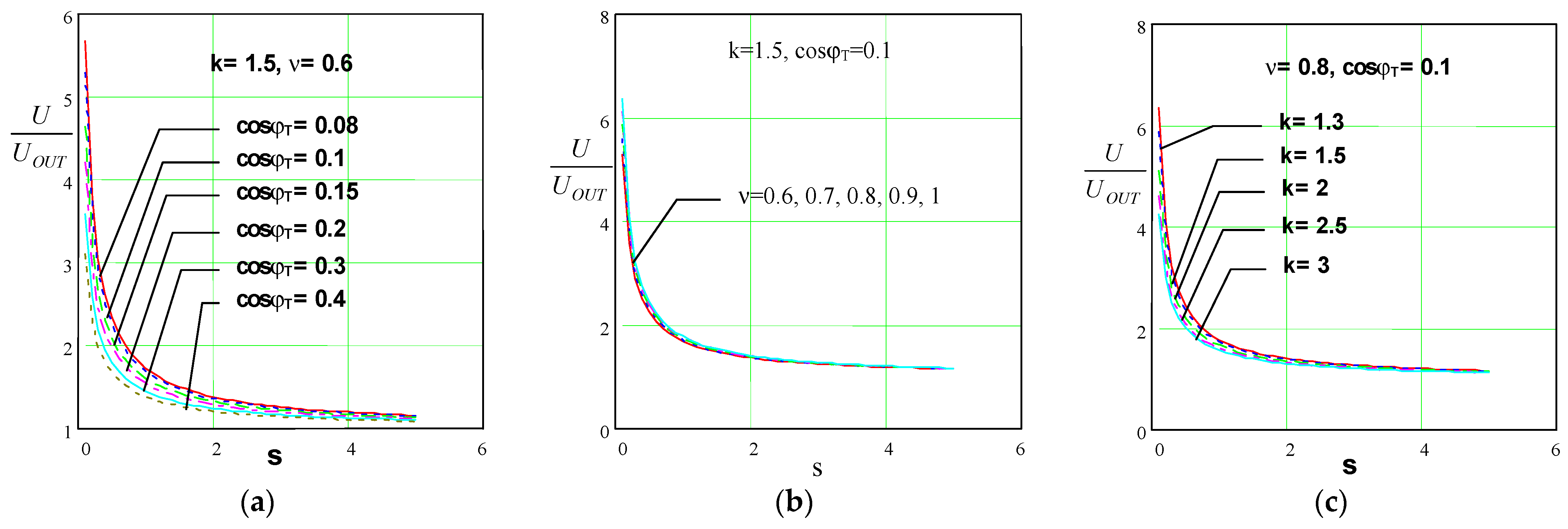
Figure 12 shows the dependence
, at parameters
k,
ν, and
cosφT during operation of the resonant inverter in soft commutation mode. The following conclusions can be drawn from it:
As cosφT decreases, the ratio U/UOUT increases.
The detuning factor ν slightly affects the ratio U/UOUT.
As the coefficient of variation increases, the U/UOUT ratio decreases.
Figure 13 shows the dependence
at parameters
k,
ν, and
cosφT when operating the resonant inverter in hard commutation mode. The following conclusions can be drawn from it:
As cosφT decreases, the ratio U/UOUT increases.
The detuning factor ν slightly affects the ratio U/UOUT.
As the slew rate increases, the U/UOUT ratio decreases.
From the look of
Figure 12 and
Figure 13, it is found that the increase in the coefficient
s leads to a decrease in the ratio
U/UOUT.
The constructed characteristics confirm the conclusions known from previous studies that the parallel-series resonant output circuit in the thus selected operating mode should be used to match the inverter and a load that requires a higher voltage than the inverted one, i.e., for powerful resonant DC/AC converters.
4.3. Series-Parallel-Parallel-Series Resonant Output Circuit
A series-parallel-parallel-series resonant output circuit is shown in
Figure 14. To obtain a series-parallel-parallel-series resonant inverter this circuit must be connected to each of the power circuits of
Figure 1 between the points labeled A and B. The same notations are used as in the previous points. It can be seen that the circuit shown in
Figure 14 can be considered as composed of series-parallel and parallel-serial output circuits. This allows the results of the previous two sections to be used to obtain the dependency
.
Similar to the previous output circuits, from the balance of the active power in the output, the dependence between the output voltage and the load voltage of the inverter is obtained:
To solve Equation (15), it is necessary to find the unknown angles γand φ. As quadratic equations are obtained for the desired unknowns, obtaining the analytical dependence becomes complex and laborious, and graphs illustrating the desired function become three-dimensional and inconvenient for rapid engineering design purposes.
In this sense, when designing resonant DC/AC converters using a series-parallel-parallel-series resonant output circuit, it is rational to use the results obtained in
Section 4.1 and
Section 4.2.
5. Design Consideration for Resonant DC/AC Converters
The design methodologies presented in this section were developed, and are based on the use of the device transfer function and and symmetry in the current shape through the AC circuit. The unified analysis of resonant DC/AC converters in different operating modes and the determination of the characteristics of the main output circuits used to match the parameters of the power electronic device and the load are the basis of the creation of engineering methodologies for the design of a whole class of power circuits.
Typically, the following initial data are set during design:
- -
the output active load power P;
- -
cosφT of the load;
- -
the RMS value of the load voltage U;
- -
output frequency f (ω).
It is also known, depending on the type of AC grid power supply and the rectifier circuit, the voltage magnitude of the DC power source.
For reasons of high efficiency and optimal loading of the semiconductor devices, the coefficient of variation
k and the detuning factor
ν are chosen. Depending on the output power and the requirements of the load, the matching method between the inverter and the load is determined. As it was already shown in
Section 3, in order to obtain operation of the resonant inverter in continuous–continuous current mode, close to the mode of an ideal current source inverter, it is necessary to choose values of coefficients
k and
ν in the range
k ≥ 2.5 and
ν ≥ 3; for the resonant inverter without reverse diodes with soft commutation, a well-harmonic composition of the current in the AC circuit is obtained at
k ≥ 1.3 and
ν ≥ 0.85; for the resonant inverter with reverse diodes, the quasi-boundary method is effective at values of the coefficients
k ≥ 1.3 and 0.85 ≤
ν ≤ 1.15.
The basis of the design methodology is the fundamental relationship between the output and input voltage of the resonant inverter (transfer function), which, depending on the operating mode and the type of power circuit, is given by expressions (7) or (8). Since these ratios differ only in the value of the coefficients, it is appropriate for design purposes to use the generalized expression:
where
The other main dependence needed for design is (6) because it relates the coefficients k and ν to the values of the inverter AC circuit elements.
In [
30] it was shown that for current source DC/AC converters, the RMS value of the output voltage, provided that a DC power source is used, obtained by rectifying a standard three-phase AC grid (without using an input grid transformer) is in the range 700 ÷ 850 V, and for resonant DC/AC converters with soft commutation by 25% lower. As already noted, higher or lower effective load voltage values are obtained either by using an output transformer or by using a multi-terminal inductor or by using complicated resonant output circuits.
On the other hand, since the main goal of the manuscript is the presentation of innovative and rational methods for the design of power electronic devices, tailored to the specifics of their operation, simplified dependencies will be used to determine the current and voltage loads of the semiconductor devices.
From the principle of operation and the analysis of resonant DC/AC converters, it is known that an estimate for the load on the semiconductor devices is given by [
28,
30]:
- -
Maximum value of the current through the devices Imax:
- -
Average value of the current through the devices Iav:
- -
Maximum voltage on the devices Umax:
- -
schematic thyristor recovery time tqc:
First, the methodology for the design of the simplest case, a parallel inverter, will be shown, and then the other commonly used matchings between the inverter and the load using complicated resonant output circuits will be considered.
5.1. Methodology for Designing Resonant DC/AC Converters with a Parallel Load Circuit
The methodology for designing a resonant DC/AC converter with a parallel compensated load was developed and is presented in this subsection. Characteristic of the parallel DC/AC converter is that the output and load voltage match, and accordingly, the angles introduced in the analysis β = γ. This predetermines its relative schematic simplicity and easy design.
- 2.
For the reasons already mentioned, depending on the specific power topology, the value of the coefficient of variation in the series resonant circuit k is chosen. The magnitude of the coefficient of variation ν is determined from formula (6):
Usually, in most practical cases with a parallel inverter, the coefficient
ρ = 1 and then expression (20) is modified into:
- 3.
Determination of the natural resonant frequency of the equivalent series resonant circuit—ω0:
- 4.
Finding the magnitude of current drawn by a DC power source—Id.
The consumed current can be determined using the results of the analysis of the particular power circuit. Since the aim of the present work is to propose a convenient and rational engineering methodology for the design of resonant DC/AC converters, another approach for its determination is proposed here. Under the assumptions made in the analysis that the efficiency factor of the inverter is unity, active power is consumed only in the load. Then for the consumed current we arrive at:
In [
29] it was proven that the results obtained using this formula do not give significant differences with those obtained using the exact expression.
- 5.
Determination of the active load resistance from the parallel load substitution circuit—Re:
- 6.
Finding the components of the load’s serial replacement circuit:
- 7.
Finding the first harmonics of the active—R(1) and reactive—X(1) components of the series substitution circuit of the inverter AC circuit (in this case a parallel load circuit):
- 8.
Determination of the damping of the series resonant circuit—δ:
- 9.
Calculation of the value of resonant inductance—LR:
- 10.
Finding the value of the load (parallel) capacity—C:
- 11.
Determination of the maximum voltage of the load capacitor—UCmax:
With the help of the already determined load in terms of current and voltage of the semiconductor devices and taking into account the operating frequencies, the power switches are selected. If necessary, a parallel and/or serial connection of devices is made.
5.2. Methodology for Design of Resonant Inverter with Series-Parallel Output Circuit
The methodology for designing a resonant DC/AC converter with sa eries-parallel compensated load was developed and is presented in this subsection. The schematic of the series-parallel resonant output circuit is shown in
Figure 6. Since it has a large overlap with the design of the parallel resonant inverter, only the differences from it will be pointed out in this subsection. Similar to the design of the parallel resonant DC/AC converter, in this case too the value of the output voltage must be chosen because it does not appear in the specification. With the assumptions thus made for the mode of operation of the series-parallel resonant output circuit, the load voltage is always lower than the output voltage.
- 2.
Finding the value of the capacity of the load (parallel) capacitor—CT:
- 3.
Determination of the value of the equivalent capacitor from the series substitution circuit of the series-parallel resonant circuit—CΣ:
- 4.
Finding the capacitance of the series capacitor—CS:
- 5.
Determination of the maximum voltage of the series capacitor—UCSmax:
The points from
Section 5.1 are used to determine the remaining quantities needed for the design of the series-parallel resonant inverter.
5.3. A Methodology for Designing a Resonant Inverter with a Parallel-Series Output Circuit
The methodology for designing a resonant DC/AC converter with a parallel-series-compensated load was developed and is presented in this subsection. The schematic of the parallel-series resonant output circuit is shown in
Figure 10. In the proposed methodology, only the differences compared to the design of the basic parallel resonant DC/AC converter circuit will be highlighted. The selection of the effective value of the output voltage is determined by the same considerations as in the previous points.
As was shown in point 4.2, the series resonant circuit composed of R, L, and CL is replaced by an impedance of series-connected active—RSER and reactive—XSER components. This impedance is converted into an equivalent consisting of parallel-connected active (1/Re) and reactive—(1/Xe) components.
- 2.
Determine the active load resistance of the equivalent load parallel replacement circuit—Re:
- 3.
Finding the first harmonics of the active (R(1)) and reactive (X(1)) components of the series substitution scheme of the AC circuit of the inverter:
- 4.
Finding the value of the load (parallel) capacity—C:
- 5.
Determining the value of series capacitance—CL:
- 6.
Determination of the maximum voltage of the series capacitor—UCLmax:
- 7.
Determination of the maximum voltage of the parallel capacitor—UCmax:
Points from
Section 5.1 are used for the calculation of the remaining quantities necessary for the design of the parallel-series resonant inverter.
5.4. Methodology for Designing a Resonant Inverter with a Series-Parallel-Parallel-Series Circuit
The methodology for designing a resonant DC/AC converter with series-parallel-parallel-series compensated load was developed and is presented in this subsection. The scheme of the series-parallel-parallel-series resonant output circuit is shown in
Figure 14. It can be considered as a combination of the series-parallel and parallel-series resonant output circuit. Analogously to the design of the other circuit varieties, taking into account the possibilities of the series-parallel circuit to reduce, respectively, the parallel-series circuit to increase its output voltage, the voltage
U’OUT is selected (
U’OUT is the voltage across the parallel capacitor
C of
Figure 14). Additionally, the value of the output voltage must be selected. In the presented methodology, only the differences compared to the case of designing a parallel resonant DC/AC converter will be highlighted.
- 2.
Determining the detuning of the parallel load circuit—γ:
As shown in the design of the parallel-series resonant inverter, the series load resonant circuit composed of R, L, and CL is replaced by an impedance of series-connected active—RSER and reactive—XSER components. This impedance is converted into an equivalent consisting of active—1/R’e and reactive—1/X’e components connected in parallel.
- 3.
Determine the active load resistance of the equivalent load parallel replacement circuit—R’e:
- 4.
Finding the first harmonics of the active (R(1)) and reactive (X(1)) components of the series replacement scheme of the parallel-series load circuit:
- 5.
Finding the value of the load (parallel) capacity—C:
- 6.
Determining the value of the series capacitance connected to the load—CL:
- 7.
Determination of the value of the equivalent capacitance from the series substitution circuit of the output circuit—CΣ:
- 8.
Finding the capacitance of the series capacitor—CS:
- 9.
Determination of the maximum voltage of the series capacitor connected to the load—UCLmax:
- 10.
Determination of the maximum voltage of the parallel capacitor—UCmax:
- 11.
Determination of the maximum voltage of the series capacitor—UCSmax:
For the calculation of the remaining quantities needed for the design of a series-parallel-parallel-series resonant inverter, the points from
Section 5.1 are used.
5.5. Methodology for Designing a Resonant Inverter with a Series Resonant Circuit
The methodology for designing a resonant DC/AC converter with series compensated load was developed and is presented in this subsection. The series resonant inverter can be with or without reverse diodes. The design is carried out in the following sequence.
The coefficients
k and
ν are chosen for considerations that were discussed in the discussion of the unified approach for the analysis of resonant DC/AC converters. Since the voltage on the series resonant circuit is formed by the switching of each of the pairs of semiconductor devices, the following relationship between the first harmonic of the output voltage and the voltage of the input DC power supply is valid [
30]:
If the value of the output voltage thus obtained does not match the requirement of the design assignment, the use of an output transformer is necessary.
- 2.
Finding the natural frequency of the series resonant circuit—ω0:
- 3.
Determination of the damping of the series resonant circuit—δ:
- 4.
Determination of the value of resonant inductance—LR:
- 5.
Calculation of the resonance capacitance value—CR:
The determination of the magnitude of the average value of the current through the devices—Iav, of the current consumed by the power source—Id, of the maximum value of the current in the alternating current circuit—Imax, is the same as in the case of a parallel resonant inverter with soft commutation.
- 6.
Determination of the maximum value of the voltage on the resonant capacitor—UCRmax:
With the help of the already determined load in terms of current and voltage of the semiconductor devices and taking into account the operating frequencies, the power switches are selected. If necessary, parallel and/or serial connection of semiconductor devices is made.
6. Results
To confirm the presented methods for designing resonant DC/AC converters with and without reverse diodes operating in different operating modes, computer simulations of transient and established modes were performed using the LTspice simulator, as well as measurements on power electronic devices manufactured by the Ultraflex power company and stands used in the educational process of the Department of “Power Electronics” at Technical University (Sofia).
Input data for design of parallel resonant DC/AC converters without reverse diodes working in the regime of soft commutation are (schematic of
Figure 1a):
- -
output active loading power P = 100 kW;
- -
load power factor cosϕT = 0.15;
- -
RMS value of loading voltage UT = 850 V;
- -
output frequency f = 4000 Hz.
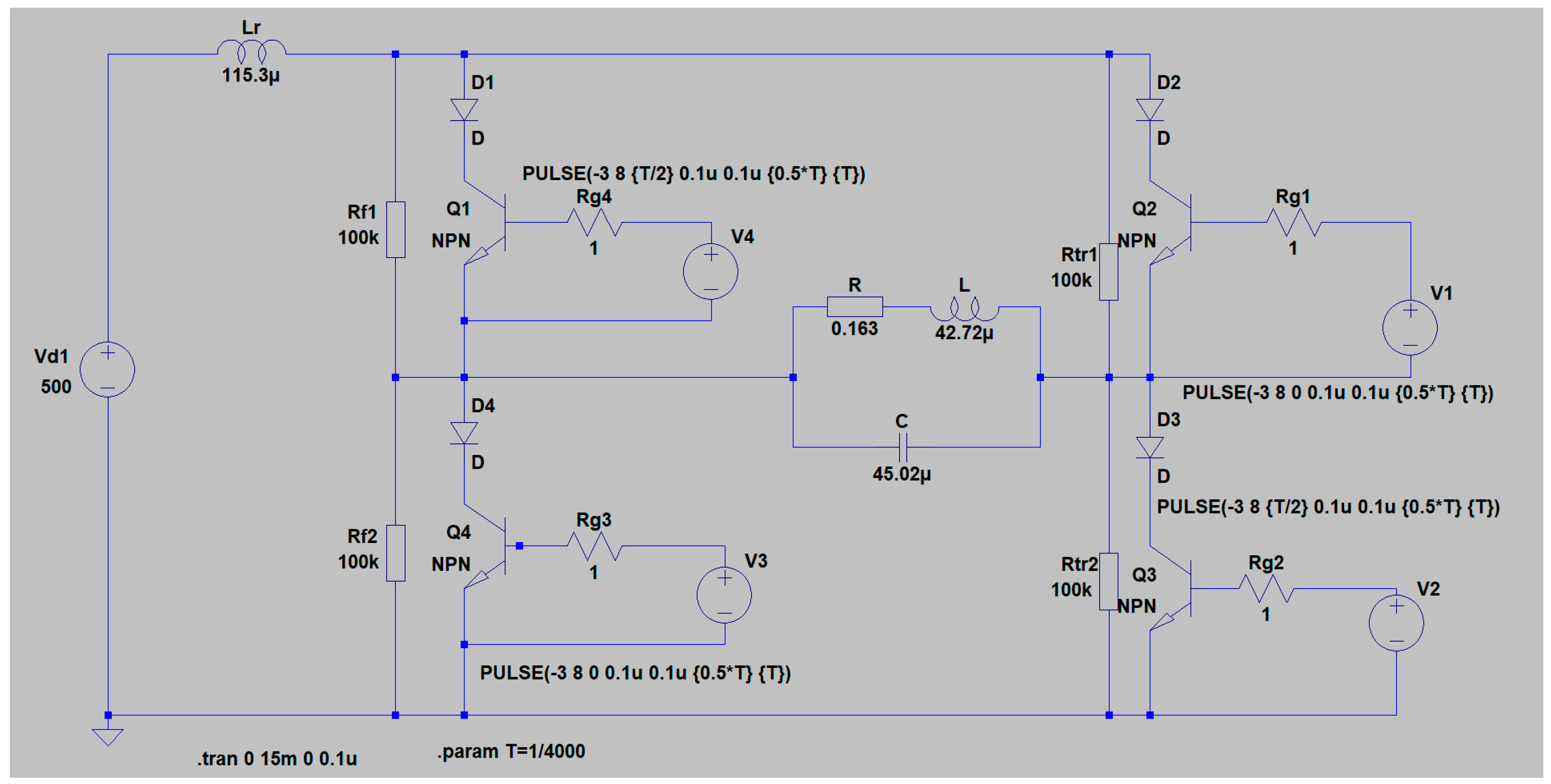
These initial design data correspond to the parameters of an induction heating device type PT-100 of the company “Promishlena Elektronika” (Gabrovo). In accordance with the design guidelines, coefficient values were selected as k = 1.5 and ν = 1. As a result of the design, the following values of the circuit elements were determined: R = 0.163 ωΩ, L = 42.72 µH, C = 45.02 µF, and LR = 115.3 µH. DC power supply value of 500 V was chosen.
Figure 15 gives simulation results of an established mode of the operation of the designed, according to the methodology presented in
Section 5.1, parallel resonant DC/AC converter. From top to bottom, some of the characteristic quantities are shown: the input current (current through the inductance)
iL, the output voltage (the voltage across the parallel capacitor
C)
UOUT, and the voltage across the thyristor VS
1—
UVS1. The LTspice model with which these results were obtained is given in a
Figure A1 in
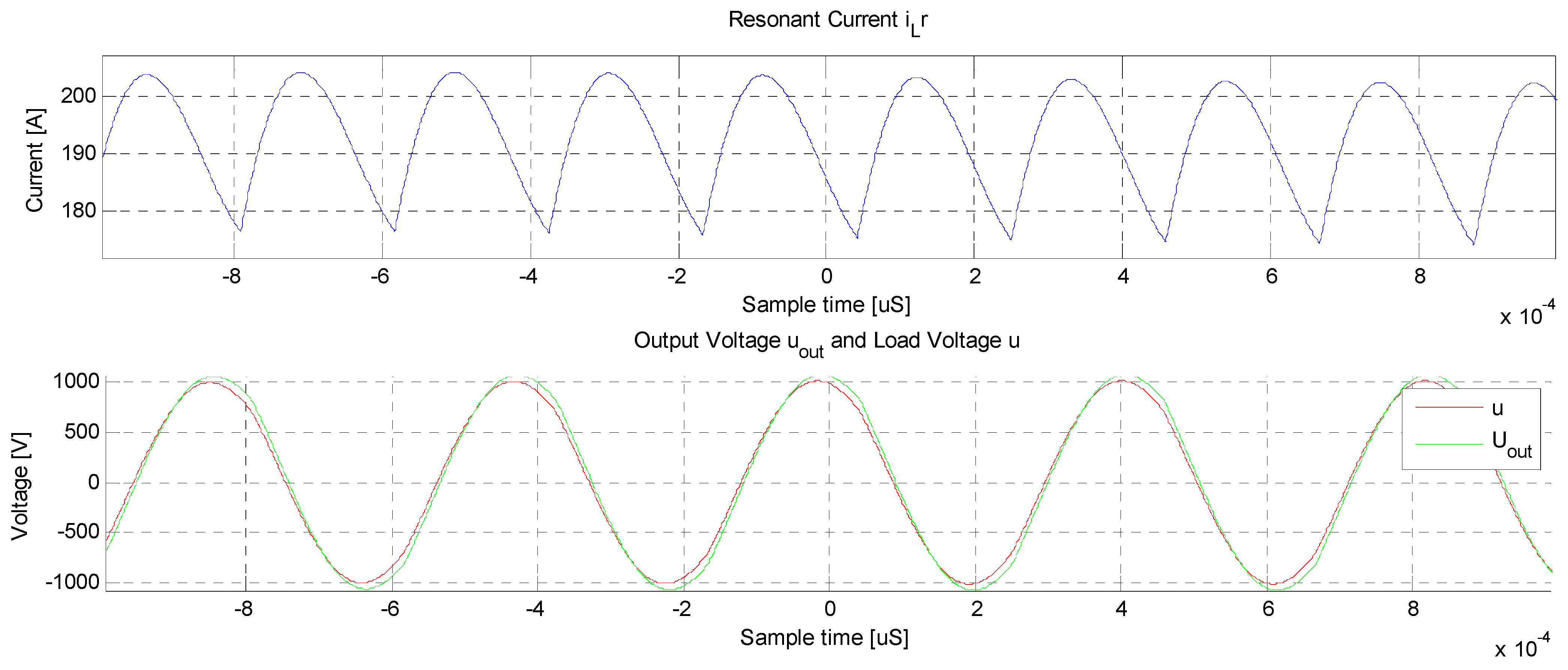
Appendix A. Due to the operation in the capacitive detuning of the parallel load circuit, there are sections with negative voltage in the voltage across the semiconductor switches. Since the power circuit is without reverse diodes, its implementation uses either thyristors or a combination of a transistor and a diode connected in series, which serves to block the supply of reverse voltage to the transistor. Since the standard libraries of the used computer simulator lack a thyristor model, a semiconductor switch composed of a series-connected bipolar NPN transistor and a diode is used for the needs of the simulations. In this way, the real operation of a thyristor is imitated without the need to install additional libraries of elements.
Figure 16 shows the experimental results of the designed power scheme. They were conducted in the test laboratory of the company “UltraFlex”, based on a modification of converters from the Ultraflex SmartPower™ Compac Systems series [
32]. To obtain the effective and average values of the required currents and voltages, the measured data are processed and visualized with specialized mathematical software developed by the company.
Table 1 presents results obtained from analytical expressions based on the proposed methodology for designing a full-bridge parallel resonant DC/AC converter from computer simulation and from experiment. The RMS, average, and maximum values of the studied quantities obtained by the simulator were determined by using its built-in functions.
Data listed in
Table 1 show that, for all values determined at design, an error is less than 5%. The difference in the results presented in
Table 1 is due to the non-sinusoidal shape of the current in the AC circuit of the inverter. In [
26,
28] it was proven that this current can be considered completely sinusoidal for values of the coefficient
k above 1.8. On the other hand, at these values of
k, which guarantee us a shape of the current in the AC circuit close to sinusoidal, large values of the output voltage and of the voltages on the semiconductor devices are obtained. Due to the large detuning angle, the reactive power consumed by the AC supply grid also increases. In this sense, the value of
k chosen during the design satisfies both the accuracy requirements of the design results and those related to the reactive power and voltage loading of the circuit elements.
The following computational example is based on the design of a resonant series-parallel inverter operating in hard commutation mode, without reverse diodes:
Input data for design of full-bridge current source DC/AC converter is:
- -
output active loading power P = 100 kW;
- -
load power factor cosφT = 0.15;
- -
RMS value of loading voltage U = 750 V;
- -
RMS value of output voltage UOUT = 800 V
- -
output frequency f = 2400 Hz.
These initial design data also correspond to the parameters of an induction heating device type PT-100 of the company “Promishlena Elektronika” (Gabrovo). In accordance with the design guidelines, the following values of the coefficients were selected: k = 2.5 and ν = 3. As a result of the design, the following values of the circuit elements were determined: R = 0.127 Ω, L = 55.32 µH, C = 88.42 µF, CS = 166.6 µF, and LR = 1.909 mH. For design purposes, a DC power supply value of 500 V was chosen.
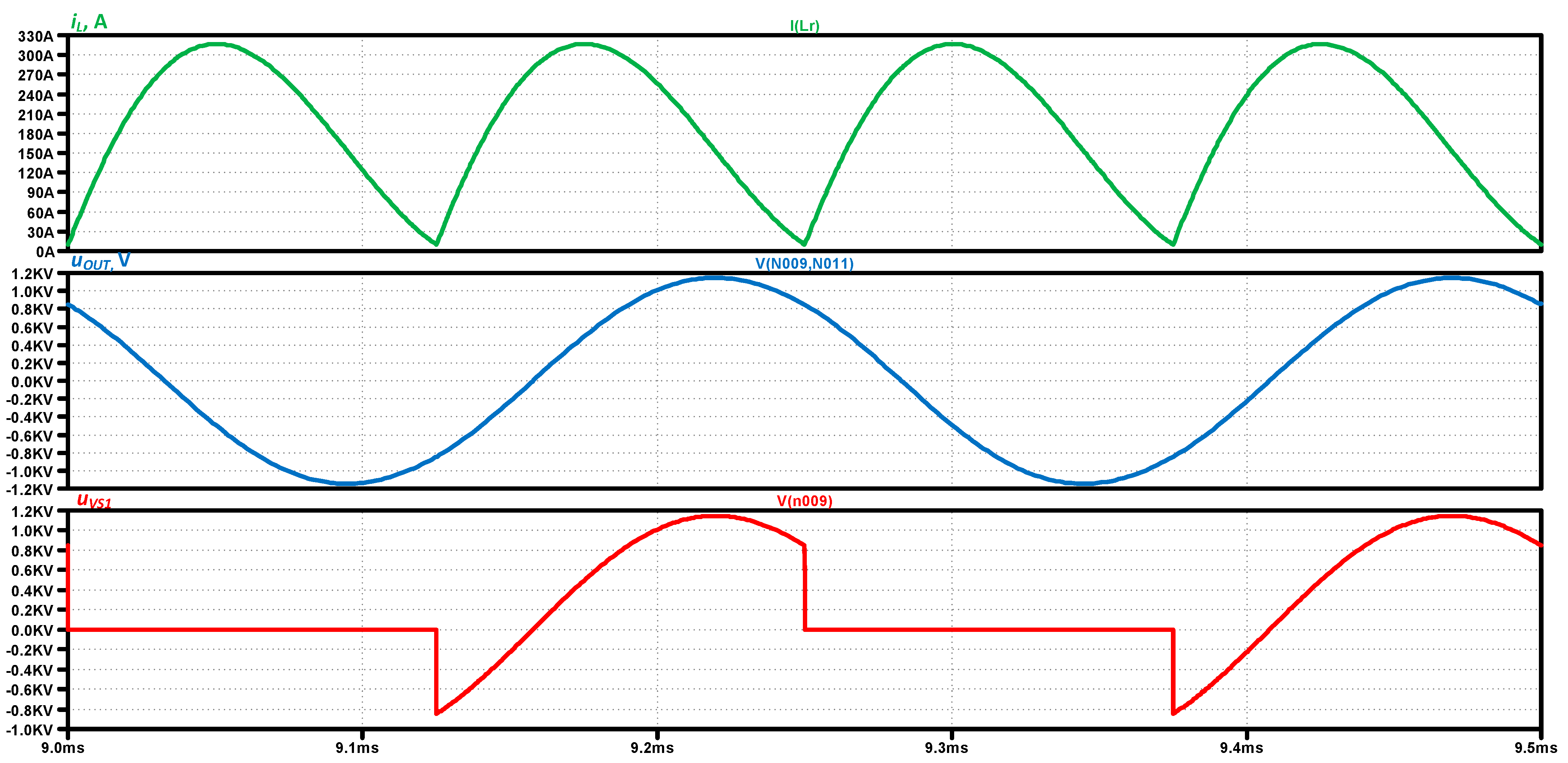
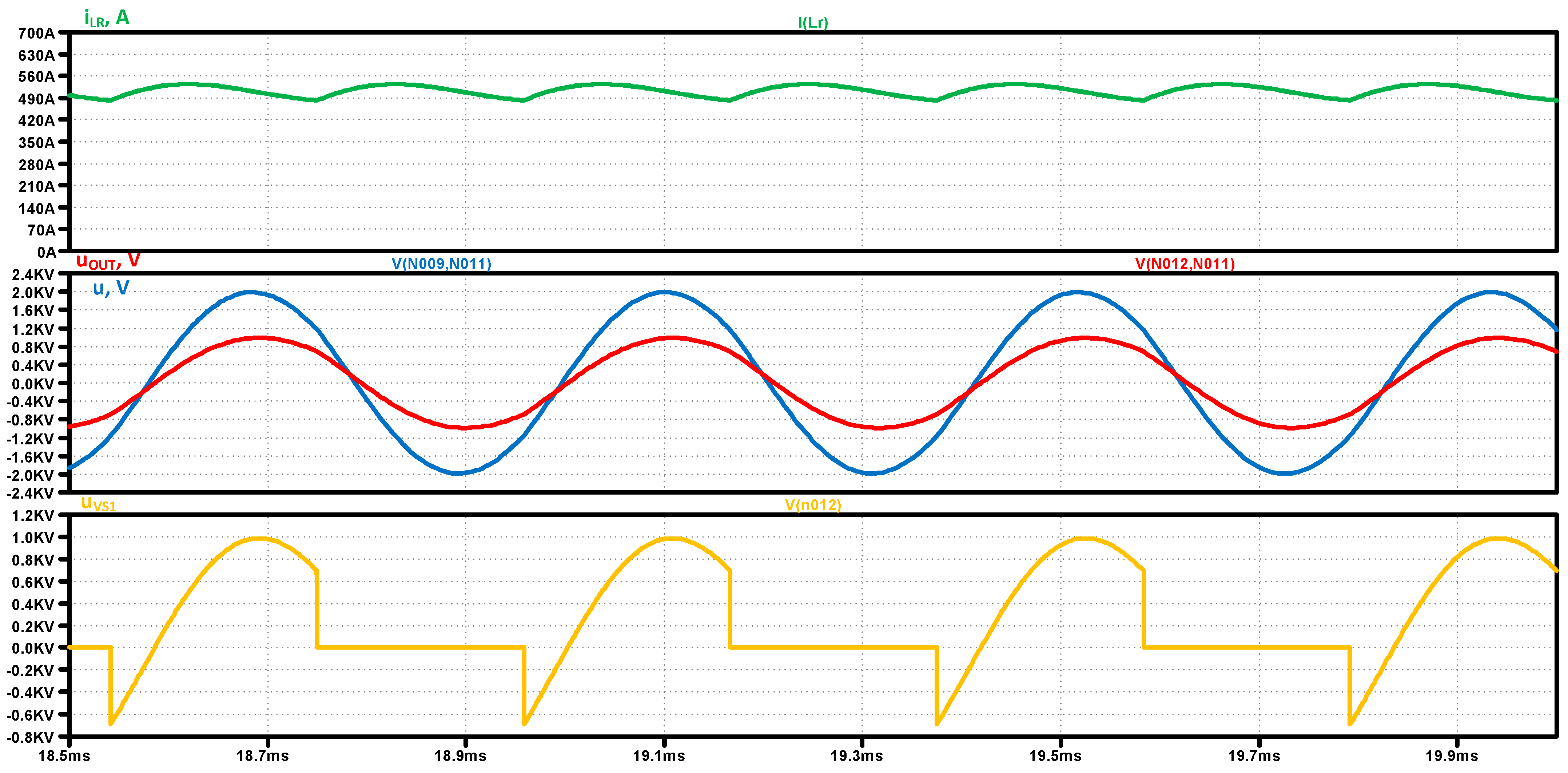
Figure 17 shows the simulation results of the study of the designed DC/AC converter; series-parallel current source inverter without reverse diodes. The input current i
L, the output voltage—
UOUT, the voltage on the load—
U, and the voltage across the thyristor VS
1—
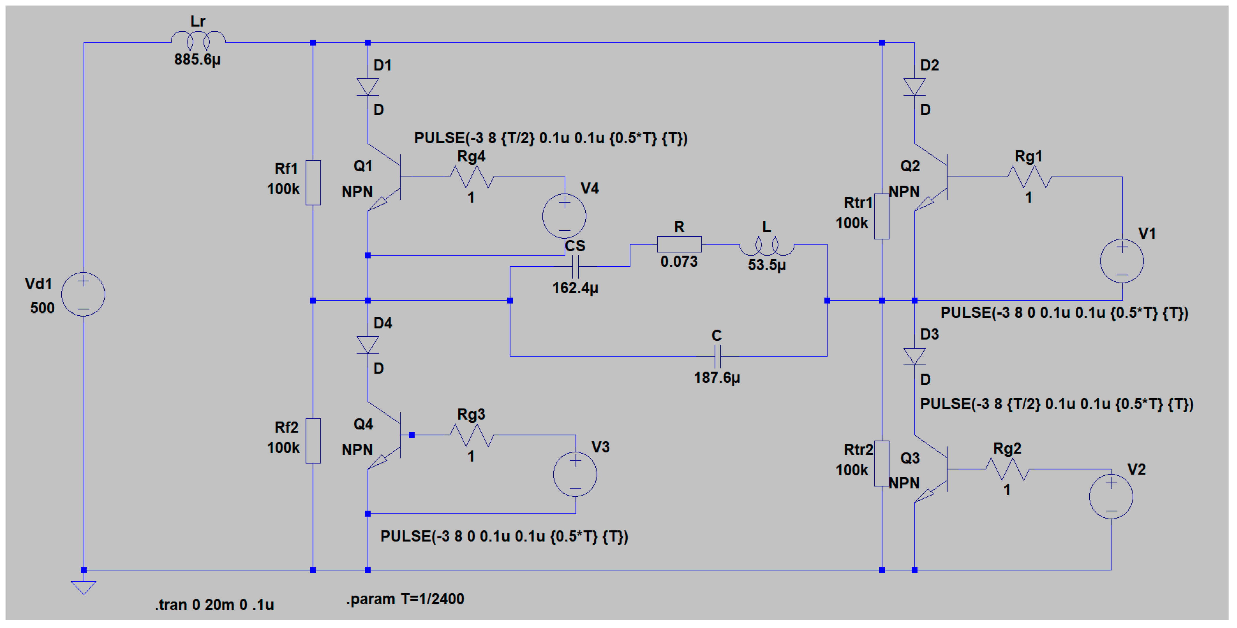
uVS1 are presented consecutively from top to bottom. The simulation model of the current sourse DC/AC converter by which the presented results were obtained is given in
Appendix A.
Figure 18 shows the experimental results of the designed power scheme. They were conducted in the test laboratory of the company “UltraFlex” based on a modification of converters from the Ultraflex SmartPower™ Compac Systems series [
32]. To obtain the effective and average values of the required currents and voltages, the measured data are processed and visualized with specialized mathematical software developed by the company.
Table 2 compares the results calculated using the proposed methodology for the design of a full-bridge series-parallel DC/AC converter with those obtained from the simulator and experiments.
The data listed in
Table 2 show that when comparing the values of the quantities obtained from design, simulations, and experiments, the difference is less than 5.5%. The difference between the simulation and analytical results is minimal (up to 3%), while in the practical it is greater, due to the tolerances of the circuit elements used and the practical impossibility of setting the calculated values of inductances and capacitors in the experiment. In this case, the difference in the results presented in
Table 2 regarding the simulations is smaller compared to the soft switching mode considered in the previous example. This is due to the fact that during the design, values of the coefficients
k and
ν were chosen, which results in insignificant deviations of the real form of the current in the AC circuit with the theoretically accepted form of the current. It is the idealized current shape that is used to determine the transfer function, according to
Figure 5. Therefore, the selected design values of
k and
ν fully satisfy the requirements for the accuracy of the design results.
The next computational example is based on the design of a parallel-series current source inverter.
Input data for the design of a full-bridge parallel-series resonant DC/AC converter operating in hard commutation mode are:
- -
output active loading power P = 250 kW;
- -
load power factor cosφT = 0.09;
- -
RMS value of loading voltage U = 1500 V;
- -
RMS value of output voltage UOUT = 750 V;
- -
output frequency f = 2400 Hz.
Selected operating mode with a switching frequency greater than the resonant frequency of the equivalent series resonant circuit; value of the detuning coefficient ν = 3.5, and the coefficient k is of value k = 2.5.
These initial design data also correspond to the parameters of an induction heating device type PT-250 of the company “Promishlena Elektronika” (Gabrovo). As a result of the design, the following values of the circuit elements were determined: R = 0.073 Ω, L = 53.5 µH, C = 187.6 µF, CL = 162.4 µF, and the resonant inductance LR = 885.6 µH. DC power supply value of 500 V was chosen.
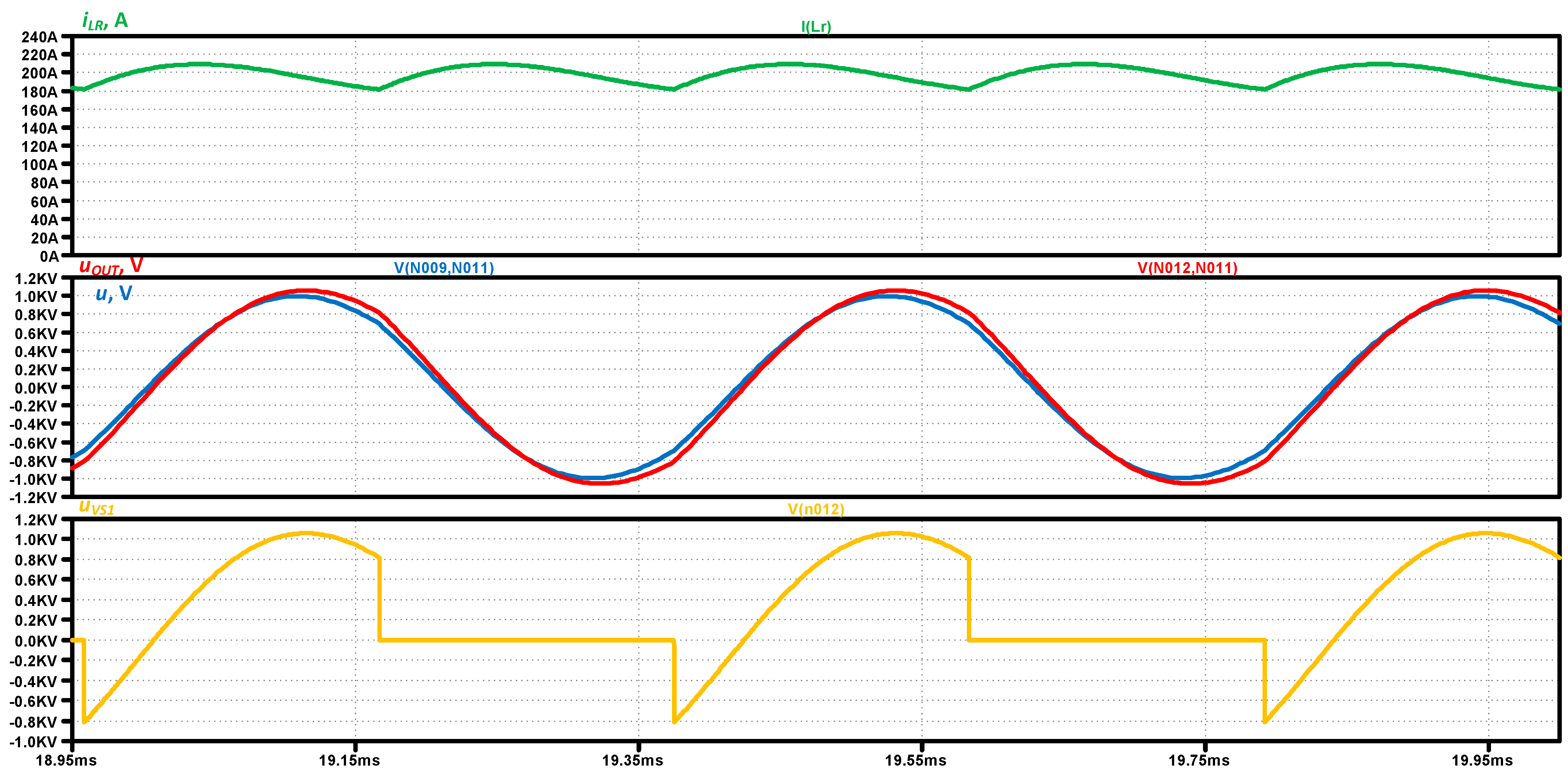
Figure 19 shows simulation results from the study of the parallel-serial current source DC/AC converter. In sequence from top to bottom, the input current
iL and the output voltage—
UOUT, the voltage on the load—
U, and the voltage across the thyristor VS
1—
uVS1 are presented. The simulation model by which these results were obtained is given in
Appendix A.
Figure 20 shows experimental test results of the designed power scheme. They were conducted in the test laboratory of the company “UltraFlex” based on modifications of power converters of the series Ultraflex SmartPower™ Compac Systems [
32]. To obtain effective and average values of the requested currents, the measured data are processed and visualized with specialized mathematical software developed by the company.
Table 3 presents results obtained from: analytical expressions based on the proposed methodology for designing a full-bridge parallel-series current source DC/AC converter from a computer simulation and from an experiment.
The data listed in
Table 3 show that when comparing the values of the quantities obtained from design, simulations, and experiments, the difference is less than 4.5%. The difference between the simulation and analytical results is minimal (up to 2.5%), while in the practical it is greater, due to the presence of the production tolerances of the building elements. In this sense, it is impossible to set the calculated values of inductances and capacitors in the experiment. In this case, the analysis of the simulation results presented in
Table 3 shows that the difference is smaller compared to the soft commutation mode and is very close in value to those of the previous example. The conclusion is confirmed that the analysis-recommended values of coefficients
k and
ν were chosen during the design, which guarantees an almost complete matching of the real current shape in the AC circuit with a rectangular shape.
The last computational example is based on the design of a transistor resonant inverter with reverse diodes (schematic of
Figure 1d). This example is discussed in detail when presenting the unified approach for the analysis of DC/AC converters [
26].
Input data for the design of a full-bridge transistor resonant inverter with reverse diodes are:
- -
output active loading power P = 10 kW;
- -
load power factor cosφT = 1;
- -
RMS value of loading voltage UOUT = 270 V;
- -
output frequency f = 50,000 Hz.
An operating mode with a switching frequency greater than the resonant frequency of the series resonant circuit is selected: value of the detuning coefficient ν = 1.1. In addition, the value of the coefficient k = 1.5 was used in the design.
As a result of the design, the following values of the circuit elements were determined:
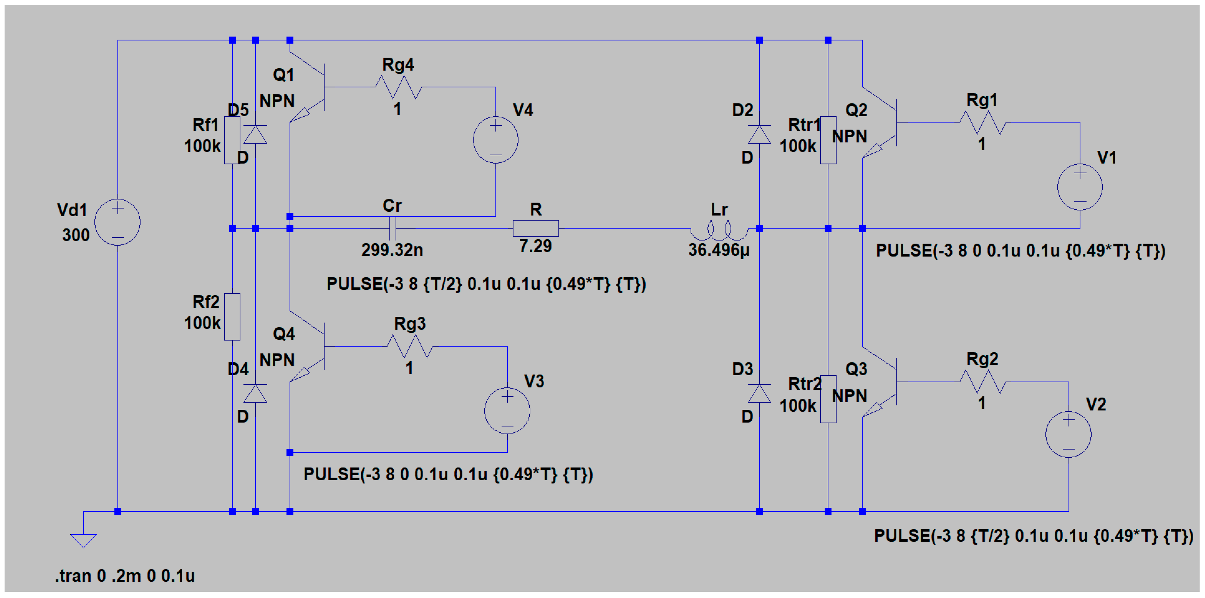
R = 7.29 Ω,
L = 36.496 µH and
C = 299.32 nF. A DC power supply value of 300 V was chosen. In this case, the practical measurements were carried out with a prototype based on a modified SOLO 10W inverter, part of an induction heating system manufactured by Ultraflex power [
33].
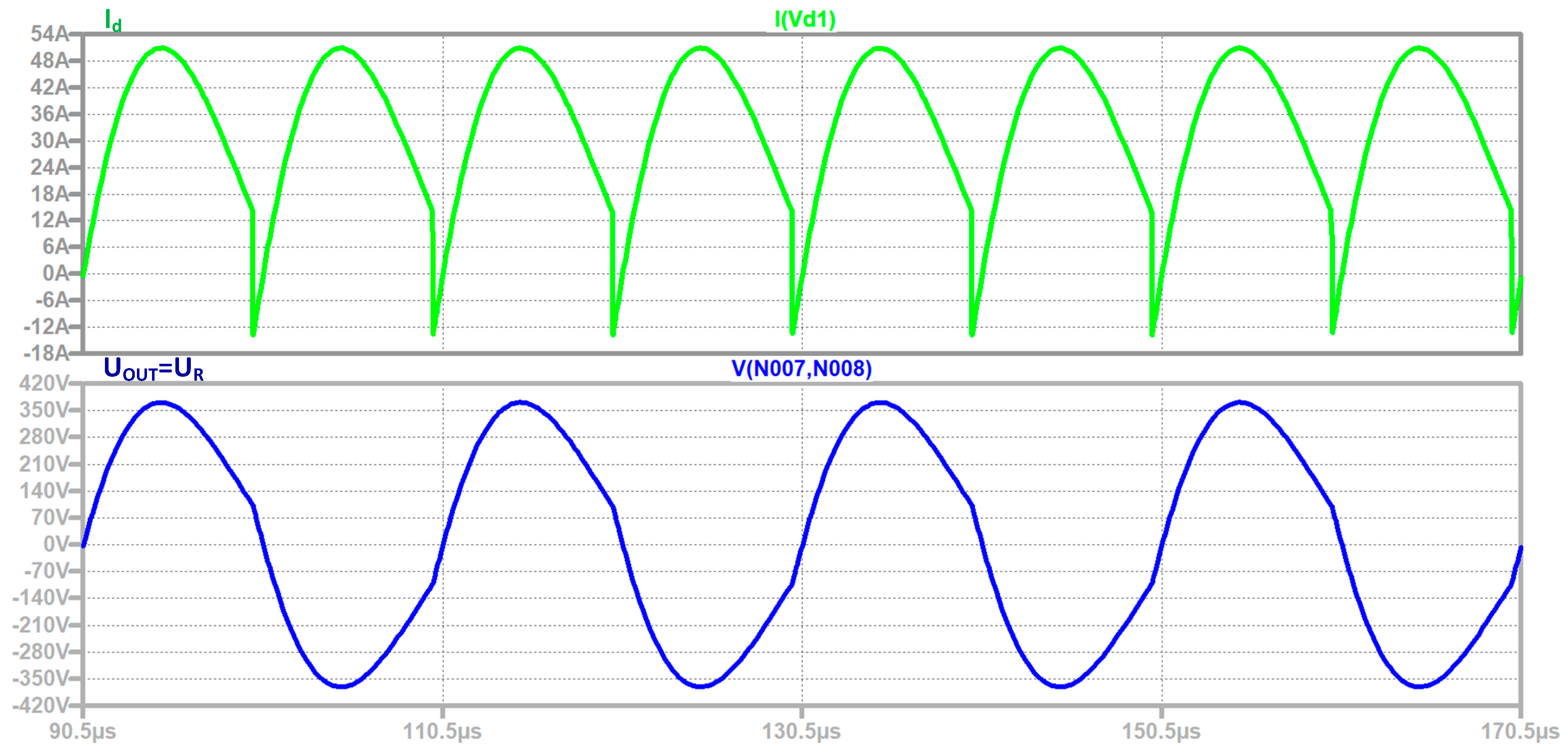
Figure 21 shows simulation results from the study of the designed series resonant DC/AC converter with reverse diodes. From top to bottom, they are presented as follows: the current consumed by the DC power source (it is formed by the sequential operation of transistors and reverse diodes) I
d and the output voltage U
OUT. From the principle of operation of the considered power topology, it is known that when the reverse diodes are turned on, the AC power from the output is fed back to the DC source. For this reason, there are negative sections in the input current waveform that correspond to the injection of energy from the AC circuit into the DC power source.
Appendix A provides the simulation model by which these results were obtained.
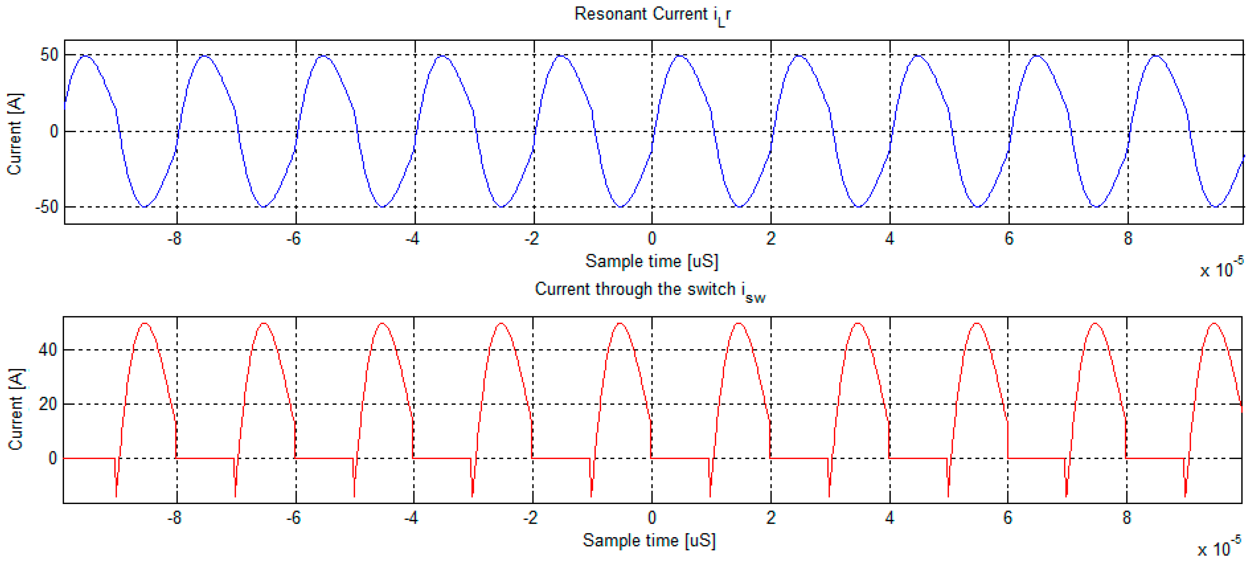
Figure 22 shows the experimental results of the designed power scheme. They were conducted in the testing laboratory of the company “UltraFlex”. To obtain the effective and average values of the required currents and voltages, the measured data are processed and visualized with specialized mathematical software developed by the company.
Table 4 presents results obtained from: analytical expressions based on the proposed methodology for designing a full-bridge resonant DC/AC converter with reverse diodes from a computer simulation and from an experiment.
Data listed in
Table 4 show that for all values determined at design, error is less than 5%. The analysis of the simulation results of
Table 4 shows that in this case, the differences between the values of the investigated quantities are the largest. This is due, on the one hand, to the non-sinusoidal shape of the current in the AC circuit of the inverter, and also to the application of the quasi-boundary method in determining the transfer function [
32]. In this sense, when designing resonant DC/AC converters with reverse diodes, in addition to the need for a certain range of coefficient
k values above 1.8, it is also necessary to ensure an operating mode with a control frequency close to the resonant frequency of the AC circuit. Regardless of these features of the power scheme, it is found that the obtained results fully satisfy the specified design accuracy.
