Abstract
A decrease in conductivity under illumination, known as negative photoconductivity, has been observed in various semiconductors and is commonly attributed to trapping of excess carriers by deep centers. Here, we demonstrate that negative photoconductivity can instead arise from a rapid increase in carrier scattering in ultranarrow-gap semiconductors with degenerate carrier statistics. This behavior is explained by the combined effects of enhanced optical phonon emission scattering and an increase in effective mass due to band filling. Experimentally, photoconductivity was measured over wide ranges of excitation and temperature in unintentionally doped n-type short-period InAsSb0.6/InAsSb0.3 strained-layer superlattices (SLS), relevant for long-wavelength infrared optoelectronic devices. The resistive device impedance, weakly dependent on excess carrier concentration, simplifies broadband impedance matching to low-voltage CMOS driver electronics. At 77 K, 10.6 µm laser excitation led to an initial rise in conductivity, with a decrease observed above 10 W/cm2.
1. Introduction
One of the distinctive properties of narrow-gap semiconductors is the small electron effective mass, which results in a low density of states (DOS) in the conduction band. For example, HgCdTe and InAsSb alloys with energy gaps V exhibit effective masses , yielding an effective DOS at the conduction band minimum below at 77 K. As a result, carrier transport in these materials is governed by degenerate carrier statistics even at relatively low electron concentrations, leading to unusual transport behavior.
In materials with degenerate carrier statistics, such as metals, the electrical conductivity is described by the Drude model and is determined by carrier mobility at the Fermi level, ,
where is the carrier concentration, is the effective mass, and is the momentum relaxation time. Under degenerate conditions, electrical transport is governed primarily by carrier scattering in the vicinity of the Fermi level and by the shape of the energy dispersion in the momentum space.
In narrow-gap semiconductors, the decrease in carrier mobility with increasing Fermi level can exceed the corresponding increase in carrier concentration. As a consequence, electrical conductivity becomes a weak function of electron concentration and can even decrease with increasing excitation at low temperatures. As shown below, when carrier scattering by optical and acoustic phonons is taken into account, excitation-induced changes in electron mobility strongly affect carrier transport, resulting in pronounced negative photoconductivity (NPC) at 77 K once the Fermi level rises more than 20 meV above the conduction band minimum. In experimental structures, this effect is partially suppressed by additional scattering from alloy disorder and ionized impurities. Unlike conventional positive photoconductivity, NPC arises when illumination enhances carrier trapping, reduces carrier mobility, or modifies electrostatic boundary conditions in a manner that outweighs photocarrier generation.
NPC has attracted sustained interest both as a fundamental transport phenomenon and as a functional effect influencing the operation of optoelectronic devices. From an application perspective, NPC has been widely reported in photodetectors and photosensitive electronic components, where it directly impacts responsivity, detectivity, noise performance, and dynamic range. NPC-enabled photodetectors have been demonstrated across a broad spectral range from ultraviolet to terahertz frequencies, in material systems such as graphene/InSe heterostructures [1], SnSe-based metal–semiconductor–metal devices [2], Bi2Se3–PtSe2 heterojunctions [3], doped ZnO thin films [4], Si/Ge and Ge nanorods [5,6], InAs nanosheets and nanowires [7,8,9,10,11,12,13], InSb nanowires [14], and porous BN nanofibers [15]. Beyond photodetection, NPC has been exploited in floating-gate phototransistors [16] and optoelectronic memory elements [17], as well as in emerging concepts such as in-sensor and visuomorphic computing architectures [18,19], highlighting its potential for multifunctional and neuromorphic device platforms.
Experimentally, NPC has been observed in a diverse range of material systems. These include narrow-gap III–V semiconductors and heterostructures already mentioned, InAs nanowires [7,8,9,10,11,12,13], InAs quantum wells [20], GaAs/AlGaAs heterostructures [21,22], quantum wells, and superlattices based on InAs/GaSb [23], InAs/AlSb [24,25], and degenerate and polar semiconductors such as InN [26] and GaN [27,28]. NPC has also been reported in oxide and chalcogenide materials, including alloys based on ZnO [4,29], ZnO/CdO [30], SnSe [2], CuO [31], and PbTe-based systems [32], and in two-dimensional and layered materials based on graphene [1,33,34], black phosphorous [34], and MoO3 [35].
The physical mechanisms underlying NPC often involve carrier trapping and photogating effects, where photoexcited carriers are captured by deep or interfacial states. Alternatively, NPC can arise from hot-carrier effects and illumination-induced carrier heating, where increased carrier temperature enhances momentum scattering. The classification and discussion on various NPC mechanisms can be found in recent reviews [36,37].
In narrow-gap and high-mobility semiconductor systems, particularly InAs-based materials and heterostructures, NPC is often especially pronounced due to strong non-equilibrium carrier dynamics and enhanced sensitivity to disorder and interface effects. These systems, therefore, provide a valuable platform for understanding NPC across material classes.
NPC observed in the InAsSb-based structures studied in this work occurs over a broad range of photon energies, including excitation near the band edge, and exhibits a fast temporal response that follows modulation frequencies up to tens of megahertz. These characteristics indicate an intrinsic transport mechanism rather than carrier trapping.
2. Approaches and Materials
a. Conductivity Modeling
Fundamentally, the conductivity of an n-type semiconductor is determined by the electron concentration and electron mobility and can be expressed as , where is energy-dependent electron concentration and is electron mobility at energy . Using the -approximation [38,39], the total conductivity can be calculated from the collision integral over all free carriers above the conduction band edge as:
Here, is the equilibrium Fermi–Dirac distribution function, and its derivative describes the non-equilibrium carrier response. The density of states is given by , the electron velocity is , and is the momentum relaxation time determined by various scattering mechanisms discussed below.
The energy dispersion relation of narrow-gap semiconductors differs significantly from the parabolic dispersion , typical of wider-gap materials. For narrow-gap semiconductors at low temperatures, the conduction band dispersion near the -valley is well described by the Kane model. The resulting non-parabolic (hyperbolic) dispersion relation can be written as:
where , and is the effective mass at the bottom of the conduction band. Near the band edge, the dispersion is hyperbolic, while at larger it approaches a quasi-linear dependence.
Under optical excitation, electron–hole pairs are generated. In narrow-gap semiconductors, photoconductivity is dominated by electrons because hole mobility is much smaller. In non-parabolic materials, optical excitation raises the Fermi level and increases the electron concentration simultaneously; however, both the effective mass and the momentum relaxation time vary strongly with the Fermi level. As a result, photoconductivity exhibits a nonlinear dependence on the Fermi energy.
In InAsSb-based materials at low temperatures, electron energy relaxation is dominated by electron–phonon interactions, including acoustic phonon scattering, deformation potential scattering, piezoelectric scattering, and polar optical phonon scattering. Among these mechanisms, acoustic phonon scattering and polar optical phonon scattering dominate at different electron energy ranges. When the electron energy reaches the optical phonon energy (approximately 25 meV above the conduction band minimum for this material), polar optical phonon emission becomes dominant over absorption, leading to a sharp reduction in the electron momentum relaxation time.
The total scattering rate due to optical phonon absorption and emission was calculated following Equations (6.89)–(6.90) on pages 249–250 from Ref. [40].
Here, and are the high-frequency and static dielectric constants, respectively, is the electron velocity, and is the optical phonon frequency. Terms proportional to describe phonon absorption, while those proportional to correspond to phonon emission, which occurs only when . Although Equation (4) is derived assuming a parabolic band, the non-parabolic dispersion of Equation (3) is substituted for to estimate the optical phonon relaxation time in narrow-gap materials.
The scattering rate due to acoustic phonons is given by:
where is the deformation potential (estimated as 6.945 eV for InAsSb0.3/InAsSb0.6 [41]), is the mass density, is the sound velocity, and is the density of states for the non-parabolic band. At liquid nitrogen temperature, the relaxation time due to acoustic phonon scattering is in ns range.
All calculations were made in Wolfram Mathematica v.11, Student Edition. Figure 1a,b shows the scattering rates for acoustic phonon and optical phonon absorption and emission, together with the effective electron mass versus Fermi energy calculated for the relevant material at T = 77 K.
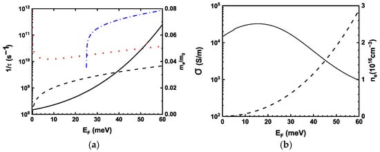
Figure 1.
(a) Carrier scattering rates on acoustical phonons, with absorption and emission of optical phonons (dashed, dotted, and dot-dashed lines, respectively), as well as electron effective mass (solid line) versus Fermi energy for the InAsSb-based compound with Eg = 70 meV at T = 77 K; (b) Dependences of electron concentration and conductivity on Fermi level at T = 77 K shown by dashed and solid lines, respectively.
The rapid increase in effective mass at higher energies leads to a strong reduction in electron mobility. Below the optical phonon energy, acoustic phonon scattering and optical phonon absorption dominate momentum relaxation; once the electron energy exceeds the phonon energy, optical phonon emission becomes the dominant scattering mechanism, reducing the relaxation time to the order of s and causing a dramatic mobility decrease.
Electron concentration and conductivity versus Fermi level at T = 77 K are shown in Figure 1b. The conductivity was calculated using Equation (2) by integrating up to an energy . Once the Fermi level exceeds 16 meV above the conduction band minimum, the conductivity at T = 77 K decreases from 3.2 S/m by a factor of 4, as the Fermi level increases to 60 meV. With the same range of EF, the electron concentration rises by an order of magnitude to approximately . However, due to the sharp reduction in relaxation time caused by optical phonon emission and the simultaneous increase in effective mass, the increase in carrier concentration is overcompensated by the decrease in mobility. In the fames of the model, in the electron concentration range above , the conductivity at T = 77 K decreases with excess carrier concentration.
Thus, although optical excitation increases the electron concentration, strong electron–phonon scattering and the energy-dependent increase in effective mass reduce the average electron mobility, leading to negative photoconductivity at elevated excitation levels. When optical phonon emission dominates energy relaxation, additional carriers contribute less to conductivity, and photoconductivity decreases despite increasing carrier density. Therefore, negative photoconductivity is an intrinsic transport property of ultranarrow-gap semiconductors in which effective mass enhancement and scattering effects are sufficiently strong to counteract carrier generation. The inclusion of additional scattering mechanisms, such as alloy disorder, leading to carrier scattering on potential fluctuations, suppresses conductivity and shifts the onset of negative photoconductivity to higher Fermi energies.
b. Heterostructure Growth, Processing, and Characterization Details
InAs1−xSbx is a promising material for long-wavelength infrared (LWIR) optoelectronics because unstrained, unrelaxed alloys with Sb compositions of 50–60% exhibit the smallest bandgap among III–V semiconductors, as low as 90 meV at K. Due to Type-2 energy band in the InAs/InAsSb system, smaller energy gaps can be realized with SLS constructed with layers with different Sb compositions [42]. The development of InAsSb-based devices is hindered by the large lattice mismatch between these alloys and commercially available substrates. To overcome this limitation, a linearly graded AlxInSb buffer layer was grown on GaSb substrate to gradually increase the lattice parameter from 6.1 to 6.24 A. Metamorphic buffers enable the growth of short-period strain-compensated unrelaxed InAsSb-based SLS to facilitate the vertical hole transport across SLS layers important for optoelectronic device applications. The composition grading facilitates threading dislocation glide and significantly suppresses dislocation propagation into the top active layer. During growth, the strain relaxation in the buffer starts from the GaSb interface side, while the upper portion of the AlInSb buffer remains unrelaxed under a residual strain. Upon reaching 57% Al composition, an in-plane lattice constant in the top of AlInSb buffer under a residual strain was 6.24 . Next, the unstrained unrelaxed A0.67lInSb 200 nm barrier was grown pseudomorphically. A 1 µm-thick InAsSb0.3/InAsSb0.6 superlattice with a 4 nm period (2 nm/2 nm layer thicknesses) was grown on the Al0.67InSb barrier. Another 200 nm thick Al0.67InSb barrier layer was subsequently grown on top of the SLS, followed by a 50 nm thick InAsSb0.3/InAsSb0.6 SLS cap layer. The wide-gap Al0.67InSb barriers provided the confinement for electrons in the narrow-gap InAsSb SLS. The lattice-matching of the barrier and SLS layers ensured the absence of dangling bonds at the AlInSb/InAsSb interfaces. The dangling bonds resulting in defect centers with energies within the energy gap lead to excess carrier recombination or trapping. Measurements of carrier recombination in similar SLS layers showed the carrier recombination time of 555 ns at 77 K, as well as a 70 ns minority hole vertical transport time across of a 2 µm SLS with no trapping [42].
The heterostructure was processed to study the lateral electron transport within the SLS layer using contacts with variable spacing [42]. The total resistance between two contacts was described with Equation (6):
where is the resistance associated with the metal–semiconductor contact, is the semiconductor conductivity, is the contact width, t is SLS thickness, and is the SLS length between the two contacts. The semiconductor conductivity was extracted from the slope of the linear relationship on L.
To fabricate the electrical contact to the SLS layer, the windows were etched through the top barrier. The surface was passivated with a 300 nm thick silicon nitride layer with windows for metal contacts. Ti/Pt/Au metal contacts were deposited and patterned using a lift-off process. In Figure 2a, the windows and the top metal layout are shown in blue and yellow colors, respectively. The silicon nitride passivation is shown in gray. The distance between adjacent metal contacts L was varied from 5 to 100 µm (5, 10, 20, 50, and 100 µm), while the contact width W was fixed at 100 µm. The top metal pads were extended over dielectric isolation to facilitate wire bonding. The schematic energy band diagram of the heterostructure with the SLS layer confined between two wide-bandgap AlInSb layers is shown in Figure 2b. The GaSb substate was polished down to a 180 µm thickness. The wafer was cleaved into 4 mm × 4 mm samples, which were mounted with a 50 µm thick indium foil on a copper block attached to a cold finger of the liquid nitrogen cooled cryostat with an uncoated ZnSe window model model Janis ST-100 from Lakeshore Cryotronics, Westerville, OH, USA. A DC bias voltage was applied between pairs of top metal contacts to facilitate the current flow in the SLS plane. The I-V characteristics were measured with the semiconductor analyzer model 4200 from Keithley, Solon, OH, USA. The photocurrent response to a pulsed excitation was measured at the wavelengths of 10.6 and 3 µm with the CO2 laser wavelength-stabilized RF-pumped laser model Merit-5 from Access Laser Company, Everett, WA, USA and with an in-house fabricated InGaAsSb/AlGaAsSb/GaSb ridge-waveguide diode laser, respectively. The diode laser current was modulated with a 50 MHz arbitrary waveform signal generator model 645 from Berkley Nucleonics Corporation, San Rafael, CA, USA. The AC photocurrent responses were measured with a 200 MHz bandwidth variable gain transimpedance amplifier model DHPCA-100 from Femto, Berlin, Germany. The responsivity spectrum was measured with the FTIR spectrometer model Nicolet Magna-860 from Thermo-Fisher Scientific, Waltham, MA, USA, with internal globar source and KBr beamsplitter.
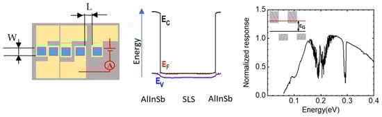
Figure 2.
(a) The top layout of the processed and cleaved sample. Th width and length of the material between the contacts are denoted with W and L, respectively; (b) The energy band diagram of the active part of the heterostructure consisting of a 4 nm period InAsSb0.6/InAsSb0.3 1-µm-thick SLS enclosed with the 200 nm-thick Al0.67InSb barrier layers for electron confinement. Ec, Ev, and EF denote the conduction and valence band edges and the Fermi level, respectively; (c) The normalized photoresponse of the SLS heterostructure at T = 77 K. The shaded areas in the inset show the conduction and valence bands of InAsSb0.3 and InAsSb0.6 layers comprising the SLS, with energy gap Eg.
3. Results and Discussion
The photoresponse spectrum under a broadband thermal source radiation from a FTIR spectrometer globar is presented in Figure 2c. The inset shows the band diagram of the SLS cell. The measured response is comparable to that of nBn detectors employing the same undoped absorber and wide-bandgap barrier materials.
In short-period SLS, the electronic states of adjacent layers are strongly coupled, so the discrete quantum-well levels broaden into minibands. Near the band edge, this results in an effective three-dimensional density of states, and the absorption coefficient, therefore, follows the usual dependence known from bulk semiconductors.
The exponential absorption tail below the band edge originates from unavoidable fluctuations of the superlattice period and alloy composition. Monolayer-scale thickness variations and local composition inhomogeneities lead to spatial fluctuations of the effective bandgap, allowing optical absorption at energies slightly below the nominal gap and producing an Urbach-like tail.
To estimate the Urbach parameter EU and the energy gap Eg of the SLS, the low-energy tail of the absorption spectrum was analyzed. The absorption coefficient was fitted using the Beer–Lambert relation,
together with the expression for direct interband transitions,
From these fits, an Urbach parameter EU meV and an effective energy gap meV were extracted.
The I–V characteristics were linear (Figure 3a). The change in the I–V slope with illumination was non-monotonic: an increase in the current (positive conductivity) was observed with room temperature illumination (RTI) estimated to be 50 mW/cm2 and with CO2 laser power densities up to 10 W/cm2. At higher power densities, the conductivity was decreasing with excitation for all gap lengths which manifested the NPC effect. The resistance between the contacts was linear with L for the contact spacing range from 20 to 100 µm (Figure 3b). This range was used for the extraction of the slope and determination of the conductivity. For contact separations of 5 and 10 µm, the measured resistance falls below the linear trend. This deviation is attributed to overlapping current-spreading regions from the two contacts when the gap becomes small compared to the contact width (100 µm), resulting in a predominantly two-dimensional current distribution and reduced effective resistance. These small-gap data were therefore excluded from conductivity extraction, which was based on the linear resistance–gap dependence at larger separations [43,44]. The reduced photoconductivity observed for contact gaps of 20 µm and below is attributed to optical near-field and diffraction effects when the electrode separation becomes comparable to the illumination wavelength (10.6 µm). In this regime, metallic contacts can partially screen the incident radiation, leading to reduced optical field intensity and absorption within the active gap region. For the gaps of 50–100 µm, where the separation exceeds the wavelength, illumination is more uniform and absorption is enhanced, resulting in higher photoconductivity.
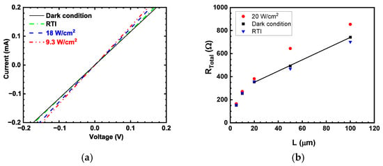
Figure 3.
(a) The I–V characteristics at T = 77 K for the contact distance of 100 µm obtained under dark conditions, RTI, and a 10.6 µm laser illumination; (b) The total resistance versus distance between the contacts under dark conditions (squares), RTI (triangles), and the 10.6 µm laser illumination with a 20 W/cm2 power density (circles). The solid line is a linear fit for the dark conditions in the gap range from 20 to 100 µm.
Figure 4a presents the dependence of conductivity on the CO2 laser power density. It is intended to demonstrate the existence and magnitude of the photoconductivity modulation rather than to establish a precise functional dependence on illumination power.
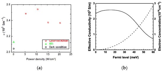
Figure 4.
(a) Dependence of the conductivity on the 10.6 µm laser power density (circles). The data for the dark and RTI conditions are shown with a square and triangle, respectively; (b) Dependence of the effective conductivity on the Fermi level obtained by with = 2.9 S/m taken to account for scattering on fluctuations of SLS potential (solid line). The electron concentration vs. the Fermi level at T = 77 K is shown for reference (dashed line).
The experimental conductivities in the range of 2–2.5 S/m were an order of magnitude smaller compared to theoretical σ-values for low EF and T = 77 K calculated from fundamental momentum scattering mechanisms (Figure 1b). The reduced experimental conductivity is attributed to elastic carrier scattering on superlattice potential fluctuations. In order to fit the experimental data in Figure 4a, that carrier scattering was modeled by an energy-independent constant = 2.9 S/m. The effective conductivity given by presented in Figure 4b showed the NPC at Fermi energies above 20 meV due to domination of optical phonon emission. The modeled data support the positive photoconductivity at lower energies corresponding to mid 1015 cm−3 and below. The background electron concentration for undoped InAsSb0.4 grown on metamorphic AlInSb buffer was reported to be 2.4 × 1015 cm−3 [45]. It was found that, at this concentration, the Fermi level is aligned with the bottom of the conduction band. Electron states with a density of 4 × 1011 cm−2 at the interface of InAsSb- and AlSb-based barriers were determined. Considering two interfaces with high power density CO2 laser excitation, the first 8 × 10¹¹ carriers per cm2 can populate the interface states, while the rest of excess carriers result in a rise in quasi-Fermi level defined by carrier lifetime in the SLS region.
The total thermal resistance of the GaSb sample of the geometry described above mounted with indium on the copper was estimated to be 0.6 K/W. Considering the laser beam diameter of 2.4 mm, the Joule overheating at the maximum laser power of 0.4 W was estimated to be less than 0.3 K, which eliminates the bolometric explanation of the NPC nature. The sign and value of the NPC effect were measured with the laser RF power supply external modulation option in on/off regime with a 100 µs rise and fall times. The modulation rate was 2.5 kHz with a 0.5 ms pulse width.
The photoconductivity at power densities up to 2 W/cm2 for the purpose of measuring the sign of conductivity and time response was measured with a 3 µm current-modulated ridge-waveguide diode laser shown in Figure 5a,b, respectively. A positive photoconductivity was observed at low excitation levels, exhibiting an approximately linear dependence on the laser power density. This behavior indicates progressive population of electronic states at the SLS/barrier interfaces under laser excitation, accompanied by an increase in the excess carrier concentration and a corresponding rise in the electron quasi-Fermi level with increasing power.
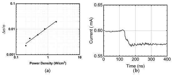
Figure 5.
(a) Dependence of the conductivity at T = 77 K measured in the range of a 3 µm diode laser power density (circles), the line shows a linear fit; (b) The time response of the conductivity measured by current modulation of the diode laser power with a 0.5 MHz repetition rate at 50% duty cycle.
In contrast to the case of free-standing InAs, where carrier capture by surface states can dominate the photoresponse [46], in SLS structures enclosed by lattice-matched AlInSb confinement layers, it is unlikely that population of interface states under high-power CO2 laser excitation can account for the observed negative photoconductivity. This conclusion is supported by quantitative estimates of the interface state density relative to the generated excess carrier concentration.
Furthermore, the characteristic tens-of-nanoseconds time scale of the photoconductivity modulation following laser excitation supports an interpretation of the negative photoconductivity in terms of a mobility reduction caused by enhanced optical phonon emission and an effective increase in the electron mass with rising excess carrier concentration.
The excess carrier concentration at high power laser excitation was estimated with a reasonable assumption of the excess carrier lifetime limited by the Auger process involving the recombination of electron–hole pair with energy transfer to another electron (CCCH process). Using the Auger coefficient Cn = 3 × 10⁻²⁴ cm6/s [47] assuming a half of the absorbed power within a 1 µm-thick SLS region with the power density of 20 W/cm2 corresponding to the excess carrier generation rate G = 1021 cm3/s, the excess carrier concentration is estimated to be n = (G/Cn)1/3 = 5 × 1015 cm−3. This translates to the quasi-Fermi level rise by 30 meV, which, according to conductivity modeling in Figure 4b, can justify the observed NPC effect.
4. Conclusions
The evidence of NPC was demonstrated by comparing resistances under dark, RTI, low-power density 3 µm diode laser and high-power density 10.6 µm CO2 laser illumination, corresponding respectively to conductivity-enhancing and conductivity-reducing regimes. Additional confirmation was provided by the dynamic conductivity response under pulsed laser excitation. In ultranarrow-gap, non-parabolic semiconductor compounds, increasing excess carrier concentration leads to an enhanced effective mass and stronger carrier scattering, resulting in a significant reduction in carrier mobility. As a result, the increase in carrier concentration was overcompensated by the rapid decrease in mobility, leading to saturation and eventual reduction in the conductivity as the quasi-Fermi level rises.
Author Contributions
Conceptualization, C.M., A.F. and D.D.; methodology, C.M., A.F., G.K., D.D. and G.B.; formal analysis, C.M., A.F., D.D. and G.B.; writing—original draft preparation, C.M.; writing—review and editing, D.D.; project administration and funding acquisition, G.B. All authors have read and agreed to the published version of the manuscript.
Funding
This research was funded by US Army Research Office through award W911NF2410232 and US Department of Energy, Office of Science, BER program, through award DE-SC0023165.
Data Availability Statement
Experimental data is available from D.D. per a reasonable request.
Conflicts of Interest
Catherine Masie is employed by Corning, Inc. The remaining authors declare that the research was conducted in the absence of any commercial or financial relationships that could be construed as a potential conflict of interest.
Abbreviations
The following abbreviations were used in this manuscript:
| NPC | negative photoconductivity |
| SLS | strained-layer superlattice |
| LWIR | long-wave infrared |
| FTIR | Fourier transform infrared spectrometer |
| RTI | room temperature illumination |
References
- Cui, B.; Xing, Y.; Niu, K.; Han, J.; Ma, H.; Lv, W.; Lei, T.; Wang, B.; Zeng, Z. Ultrahigh responsive negative photoconductivity photodetector based on multilayer graphene/InSe van der Waals heterostructure. J. Sci. Adv. Mater. Devices 2022, 7, 100484. [Google Scholar] [CrossRef]
- Rani, S.; Das, S.; Siddiqui, S.A.; Jain, A.; Rani, D.; Pahuja, M.; Chaudhary, N.; Afshan, M.; Ghosh, R.; Swadia, D.; et al. Harnessing environmental sensitivity in SnSe-based metal–semiconductor–metal devices: Unveiling negative photoconductivity for enhanced photodetector performance and humidity sensing. ACS Appl. Mater. Interfaces 2024, 16, 26899–26914. [Google Scholar] [CrossRef]
- Shu, T.; Tan, C.; Hu, G.; Luo, S.; Wang, Z. Bi2Se3–PtSe2 heterostructure ultrabroadband UV-to-THz negative photoconductive photodetectors. Nanoscale 2025, 17, 12786–12796. [Google Scholar] [CrossRef]
- Mzoughi, T.; Ben Amor, F.; Hamrouni, A.; Hamdaoui, N. Negative photoconductivity and high detectivity in Ba-doped ZnO UV photodetectors. Ceram. Int. 2024, 50, 49011–49020. [Google Scholar] [CrossRef]
- Yakimov, A.I.; Dvurechenskii, A.V.; Nikiforov, A.I.; Pchelyakov, O.P. Negative interband photoconductivity in Ge/Si heterostructures with type-II quantum dots. JETP Lett. 2000, 72, 186–189. [Google Scholar] [CrossRef]
- John, J.W.; Dhyani, V.; Georgiev, Y.M.; Gangnaik, A.S.; Biswas, S.; Holmes, J.D.; Das, A.K.; Ray, S.K.; Das, S. Ultrahigh negative infrared photoconductance in As-doped Ge nanowires induced by hot-electron trapping. ACS Appl. Electron. Mater. 2020, 2, 1934–1942. [Google Scholar] [CrossRef]
- Wang, X.; Pan, D.; Sun, M.; Lyu, F.; Zhao, J.; Chen, Q. High-performance room-temperature UV–IR photodetector based on InAs nanosheets with wavelength- and intensity-dependent negative photoconductivity. ACS Appl. Mater. Interfaces 2021, 13, 26187–26195. [Google Scholar] [CrossRef]
- Zhang, X.; Liu, Y.; Wang, Z.; Li, J.; Chen, Q. Negative photoconductive effects in uncooled InAs nanowire photodetectors. Front. Phys. 2021, 9, 725680. [Google Scholar] [CrossRef]
- Shen, L.; Yip, S.P.; Lan, C.; Shu, L.; Li, D.; Zhou, Z.; Wong, C.-Y.; Pun, E.Y.B.; Ho, J.C. Enhanced negative photoconductivity in InAs nanowire phototransistors surface-modified with molecular monolayers. Adv. Mater. Interfaces 2018, 5, 1701104. [Google Scholar] [CrossRef]
- Yang, Y.; Peng, X.; Kim, H.-S.; Kim, T.; Jeon, S.; Kang, H.K.; Choi, W.; Song, J.; Doh, Y.-J.; Yu, D. Hot-carrier trapping induced negative photoconductance in InAs nanowires. Nano Lett. 2015, 15, 5875–5882. [Google Scholar] [CrossRef] [PubMed]
- Han, Y.; Zheng, X.; Fu, M.; Pan, D.; Li, X.; Guo, Y.; Zhao, J.; Chen, Q. Negative photoconductivity of InAs nanowires. Phys. Chem. Chem. Phys. 2016, 18, 818–826. [Google Scholar] [CrossRef]
- Han, Y.; Fu, M.; Tang, Z.; Zheng, X.; Ji, X.; Wang, X.; Lin, W.; Yang, T.; Chen, Q. Switching from negative to positive photoconductivity toward intrinsic photoelectric response in InAs nanowires. ACS Appl. Mater. Interfaces 2017, 9, 2867–2874. [Google Scholar] [CrossRef]
- Alexander-Webber, J.A.; Groschner, C.K.; Sagade, A.A.; Tainter, G.; Gonzalez-Zalba, M.F.; Di Pietro, R.; Wong-Leung, J.; Tan, H.H.; Jagadish, C.; Hofmann, S.; et al. Engineering the photoresponse of InAs nanowires. ACS Appl. Mater. Interfaces 2017, 9, 43993–44000. [Google Scholar] [CrossRef] [PubMed]
- Xu, R.; Sun, Y.; Zhu, Y.; Wang, F.; Wang, J.; Cheng, L.; Xu, K.; Qian, Y. Switchable photoconductance of colloidal InSb nanowires enabled by tunable surface band bending. Appl. Surf. Sci. 2024, 670, 160690. [Google Scholar] [CrossRef]
- Zhang, S.; Lin, J.; Li, C.; Shuang, S.; Yu, C.; Tang, C.; Huang, Y. Negative photoconductivity in porous boron nitride nanofibers. ACS Photonics 2025, 12, 5649–5657. [Google Scholar] [CrossRef]
- Wang, Y.; Liu, E.; Gao, A.; Cao, T.; Long, M.; Pan, C.; Zhang, L.; Zeng, J.; Wang, C.-Y.; Hu, W.; et al. Negative photoconductance in van der Waals heterostructure-based floating-gate phototransistors. ACS Nano 2018, 12, 9513–9520. [Google Scholar] [CrossRef]
- Kumar, A.; Intonti, K.; Viscardi, L.; Durante, O.; Pelella, A.; Kharsah, O.; Sleziona, S.; Giubileo, F.; Martucciello, N.; Ciambelli, P.; et al. Coexistence of positive and negative photoconductivity and memory effects in low-dimensional semiconductors. Mater. Horiz. 2024, 11, 1234–1246. [Google Scholar] [CrossRef]
- Xu, Y.; Xu, X.; Huang, Y.; Tian, Y.; Cheng, M.; Deng, J.; Xie, Y.; Zhang, Y.; Zhang, P.; Wang, X.; et al. Gate-tunable positive and negative photoconductance in near-infrared organic heterostructures for in-sensor computing. Adv. Mater. 2024, 36, 2470235. [Google Scholar] [CrossRef]
- Wang, L.; Wang, H.; Liu, J.; Wang, Y.; Shao, H.; Li, W.; Yi, M.; Ling, H.; Xie, L.; Huang, W. Negative photoconductivity transistors for visuomorphic computing. Adv. Mater. 2024, 36, 2403538. [Google Scholar] [CrossRef]
- Lo, I.; Mitchel, W.C.; Manasreh, M.O.; Slutz, C.E.; Evans, K.R. Negative persistent photoconductivity in AlGaSb/InAs quantum wells. Appl. Phys. Lett. 1992, 60, 751–753. [Google Scholar] [CrossRef]
- Hopfel, R.A. Spectral photoconductivity in modulation-doped GaAs/AlGaAs quantum wells. Appl. Phys. Lett. 1987, 51, 106–108. [Google Scholar] [CrossRef]
- Minina, N.Y.; Bogdanov, E.V.; Il’evskiĭ, A.A.; Kraak, W. Relaxation of low-temperature negative photoconductivity in p-GaAs/AlGaAs heterostructures. Phys. Solid State 2006, 48, 2216–2219. [Google Scholar] [CrossRef]
- Schets, H.; Janssen, P.; Witters, J.; Borghs, S. Negative persistent photoconductivity in an InAs/GaSb quantum well. Solid State Commun. 1999, 110, 169–171. [Google Scholar] [CrossRef]
- Aleshkin, V.Y.; Gavrilenko, V.I.; Gaponova, D.M.; Ikonnikov, A.V.; Marem’yanin, K.V.; Morozov, S.V.; Sadofyev, Y.G.; Johnson, S.; Zhang, Y.-H. Spectra of persistent photoconductivity in InAs/AlSb quantum wells. Semiconductors 2005, 39, 22–26. [Google Scholar] [CrossRef]
- Sadofyev, Y.G.; Ramamoorthy, A.; Bird, J.P.; Johnson, S.R.; Zhang, Y.-H. Large negative persistent photoconductivity in InAs/AlSb quantum wells. Appl. Phys. Lett. 2005, 86, 192109. [Google Scholar] [CrossRef]
- Wei, P.-C.; Chattopadhyay, S.; Yang, M.-D.; Tong, S.-C.; Shen, J.-L.; Lu, C.-Y.; Shih, H.-C.; Chen, L.-C.; Chen, K.-H. Room-temperature negative photoconductivity in degenerate InN thin films. Phys. Rev. B 2010, 81, 045306. [Google Scholar] [CrossRef]
- Matys, M.; Yamada, A.; Ohki, T.; Tsunoda, K. Transition from positive to negative photoconductivity in AlGaN/GaN quantum-well heterostructures. arXiv 2025, arXiv:2504.15536. [Google Scholar]
- Su, Z.G.; Xu, J.T.; Chen, J.; Li, X.Y.; Liu, J.; Zhao, D.G. Negative persistent photoconductivity in unintentionally doped n-type GaN. Chin. J. Semicond. 2007, 28, 878–882. [Google Scholar]
- Kavasoglu, N.; Kavasoglu, A.S.; Okti, S. Observation of negative photoconductivity in (ZnO)x(CdO)1−x films. J. Phys. Chem. Solids 2009, 70, 521–526. [Google Scholar] [CrossRef]
- Yadav, H.; Sreenivas, K.; Gupta, V. Persistent photoconductivity due to trapping of induced charges in Sn/ZnO thin-film UV photodetectors. Appl. Phys. Lett. 2010, 96, 223507. [Google Scholar] [CrossRef]
- Bhunia, A.K.; Sen, S.; Guha, P.K.; Saha, S. Negative photoconductivity in PVP-encapsulated CuO nanorods. Eur. Phys. J. Plus 2023, 138, 613. [Google Scholar] [CrossRef]
- Akimov, B.A.; Bogoyavlenskiy, V.A.; Ryabova, L.I.; Vasil’kov, V.N. Negative photoconductivity in n-PbTe(Ga) epitaxial films. Phys. Rev. B 2000, 61, 16045. [Google Scholar] [CrossRef]
- Ryzhii, V.; Ryzhii, M.; Ponomarev, D.S.; Leiman, V.G.; Mitin, V.; Shur, M.S.; Otsuji, T. Negative photoconductivity and hot-carrier bolometric detection of terahertz radiation in graphene–phosphorene hybrids. arXiv 2018, arXiv:1808.09083. [Google Scholar]
- Heyman, J.N.; Stein, J.D.; Kaminski, Z.S.; Banman, A.R.; Massari, A.M.; Robinson, J.T. Carrier heating and negative photoconductivity in graphene. J. Appl. Phys. 2015, 117, 013101. [Google Scholar] [CrossRef]
- Basyooni, M.A.; Kabatas, M.; Zaki, S.E.; Rahmani, K.; En-Nadir, R.; Eker, Y.R. Negative photoconductivity in 2D α-MoO3/Ir self-powered photodetectors. Materials 2023, 16, 6756. [Google Scholar] [CrossRef]
- Tailor, N.K.; Aranda, C.A.; Saliba, M.; Satapathi, S. Negative photoconductivity: Bizarre physics in semiconductors. ACS Mater. Lett. 2022, 4, 2298–2320. [Google Scholar] [CrossRef]
- Bi, X.-Y.; Li, K.-H.; Song, Y.-J.; Zou, Y.; Xia, P.; Sun, F.; Wu, J.-Y.; Zhang, X.-Y.; Zhang, T. Negative Photoconductivity in 2D Materials: Revolutionizing Adaptive Optoelectronic Intelligence and Secure Information Architectures. Small 2025, 21, e06764. [Google Scholar] [CrossRef]
- Grimvall, G. The Electron-Phonon Interaction in Metals; Elsevier Science: New York, NY, USA, 1981; p. 207. [Google Scholar]
- Gantmakher, V.F.; Levinson, Y.B. Modern Problems in Condensed Matter Science-19; Elsevier Science: Amsterdam, The Netherlands, 1987; p. 168. [Google Scholar]
- Singh, J. Electronic and Optoelectronic Properties of Semiconductor Structures; Cambridge University Press (CUP): Cambridge, NY, USA, 2003; pp. 241–256. [Google Scholar]
- Vurgaftman, I.; Mayer, J.R.; Ram-Mohan, L.R. Band parameters for III-V compound semiconductors and their alloys. J. Appl. Phys. 2001, 89, 5815–5875. [Google Scholar] [CrossRef]
- Liu, J.; Donetski, D.; Kucharczyk, K.; Zhao, J.; Kipshidze, G.; Belenky, G.; Svensson, S.P. Short-period InAsSb-based strained layer superlattices for high quantum efficiency long-wave infrared detectors. Appl. Phys. Lett. 2022, 120, 141101. [Google Scholar] [CrossRef]
- Schroder, D.K. Semiconductor Material and Device Characterization; John Wiley & Sons: Hoboken, NJ, USA, 2006; p. 131. [Google Scholar]
- Reeves, G.K.; Harrison, H.B. Obtaining the specific contact resistance from transmission line model measurements. IEEE Electron Device Lett. 1982, 3, 111–113. [Google Scholar] [CrossRef]
- Svensson, S.P.; Crowne, F.J.; Hier, H.S.; Sarney, W.L.; Beck, W.A.; Lin, Y.; Donetsky, D.; Suchalkin, S.; Belenky, G. Background and interface electron populations in InAs0.58Sb0.42. Semicond. Sci. Technol. 2015, 30, 035018. [Google Scholar] [CrossRef]
- Pelella, A.; Demontis, V.; Sessa, A.; Mazzotti, A.; Giubileo, F.; Zannier, V.; Sorba, L.; Rossella, F.; Di Bartolomeo, A. Photogating in Suspended InAs Nanowire Field Effect Transistors for Neuromorphic Applications. Adv. Electron. Mater. 2025, 11, 00520. [Google Scholar] [CrossRef]
- Aytac, Y.; Olson, B.V.; Kim, J.K.; Shaner, E.A.; Hawkins, S.D.; Klem, J.F.; Olesberg, J.; Flatté, M.E.; Boggess, T.F. Bandgap and temperature dependence of Auger recombination in InAs/InAsSb type-II superlattices. J. Appl. Phys. 2016, 119, 215705. [Google Scholar] [CrossRef]


Disclaimer/Publisher’s Note: The statements, opinions and data contained in all publications are solely those of the individual author(s) and contributor(s) and not of MDPI and/or the editor(s). MDPI and/or the editor(s) disclaim responsibility for any injury to people or property resulting from any ideas, methods, instructions or products referred to in the content. |
© 2026 by the authors. Licensee MDPI, Basel, Switzerland. This article is an open access article distributed under the terms and conditions of the Creative Commons Attribution (CC BY) license.