Article

Effect of Surface Texture on Light Extraction Efficiency for LEDs

Institute of Photonics Engineering, National Kaohsiung University of Science and Technology, Kaohsiung 82445, Taiwan
Crystals 2023, 13(3), 491; https://doi.org/10.3390/cryst13030491
Submission received: 10 January 2023 / Revised: 3 March 2023 / Accepted: 9 March 2023 / Published: 12 March 2023
(This article belongs to the Special Issue Optoelectronics and Photonics in Crystals)

Abstract

:
The light extraction efficiency of an LED is dependent on its surface texture. However, the surface of the p-GaN layer is not easy to be etch with inverted hexagonal pyramid structures (IHPS) with small top widths and large depths using existing methods. Therefore, it is important to discuss the expected effect of the conditions of thermal annealing and inductively coupled plasma (ICP) reactive ion etching (RIE) for the generation of nano-pin-holes in the photoresist and fabrication of the top surface structure of GaN-based LEDs, in order to enhance the light output power. In this study, the following four items will be discussed: (1) the effect of thermal annealing on the composition of the photoresist; (2) the effect of thermal annealing and ICP RIE on the generation of the nano-pin-holes in the photoresist; (3) the effect of ICP RIE on the IHPS; and (4) the effect of surface texture of the IHPS on the light output power. It has been found that a nano-pin-hole structure in the photoresist etching mask is needed for the fabrication of many IHPS on the LED surface. A maskless via-hole etching technique was used for texturing the photoresist to produce nano-pore structures with diameters of less than 50 nm. The relationship between the light extraction efficiency and the surface texture is discussed in detail. The simulation results show the best light extraction efficiency (LEE) ratio of 358% to be obtained when the distance between two neighboring IHPS patterns (DBNP) is 300 nm. This in turn allowed the formation of IHPS with small top widths and large depths on the LED surface. A LEE ratio of 305% was obtained with the fabrication of IHPS with a top width of 290 nm, a depth of 170 nm and a DBNP of 180 nm on the LED surface.

1. Introduction

High-brightness LEDs are required for solid-state lighting applications, such as in automotive headlamps, full-color outdoor displays, traffic lights, etc. One of the problems with conventional GaN-based LEDs is that the large difference between the refractive indices of the LED (2.5) and the surrounding air (1.0) causes most of the light to be reflected and then absorbed before it can escape from the semiconductor. The light output power of the LED is affected by the texture of the top surface [1,2,3,4,5,6]. A variety of techniques have been used for the purpose of surface texturing, including wet etching [7,8], dry etching [9], the formation of textured n-GaN layers [10] and photonic crystalline structures [11]. Several methods for the fabrication of V-shaped textures [9,12,13,14,15] on the surface of LEDs have also been developed in order to enhance their light output powers. For example, an enhancement in the light output power value of 0.486 times that of the conventional LED (CLED) was observed after the deposition of V-shaped pits about 600 nm in diameter [13,14]. Additionally, three-dimensional GaN truncated pyramid structures, using a self-aligned twofold epitaxial lateral overgrowth technique, were fabricated with an air void and a SiO2 layer [16]. Simulation results [17] have shown truncated cone arrays with a top radius of less than 0.4 μm to be preferable. Past studies indicate that the light extraction efficiency (LEE) can be enhanced by texturing the LED surface. However, texturing the top surface of p-GaN to obtain IHPS with top widths of less than 0.4 μm and depths deeper than 150 nm is not easy using existing methods, as shown by the lack of studies in the literature detailing optimally designed IHPS surface textures to enhance LEE and which type of LED surface texture can be expected to result in the best LEE. LED chips must be cheap to produce and easy to fabricate, but still have high LEE. Using an optical stepper to generate nanometer patterns or holes in the photoresist for the fabrication of a semiconductor is too expensive, and the production speed is too slow. Some maskless methods were used. For example, using SiN treatment without a conventional nano lithography imprint method for patterning sapphire substrate, patterning AlxGa1−xN epilayers were naturally grown [18,19]. Therefore, in this study, it could be best to use a maskless method for the formation of a nano-pore structure in the photoresist (i.e., texturing the photoresist to generate holes of less than 100 nm), itself to be used as the etching mask for texturing the top surface of the LED. However, up to now, the correct size of pore structure required in the photoresist etching mask to fabricate IHPS with small top widths on the LED surface has been unknown. The relationshop between the LEE and the surface texture needs to be examined. This is the first time that the effect of the process conditions on the top surface of the structure will be discussed.

2. Experimental Details

The structure of the LED comprised a 200 nm thick undoped GaN layer, a 2400 nm thick Si-doped n-GaN layer, 8 pairs of InGaN/GaN multiple-quantum wells, a 30 nm thick Mg-doped p-AlGaN layer, a 165 nm thick Mg-doped GaN layer, a 5 nm thick p-InGaN contact layer, a 300 nm thick ITO layer, and an 80 nm thick SiO2 layer. The ITO and SiO2 layers were coated using a sputtering system [20,21,22,23,24,25]. A 1200 nm thick photoresist (AZ6112) layer was spin-coated onto the p-GaN layer at a speed of 3000 rpm. The following processes were then carried out: samples were baked (at 120–280 °C) for 10–70 min, followed by inductively coupled plasma (ICP) reactive ion etching (RIE) for 20–60 s. Measurements were made by field emission scanning electron microscopy and film X-ray diffraction (XRD). The finite element method (FEM) used for the simulations has been described in detail in a previous report [26,27]. The current vs. light intensity relationship (I-L) of the LED was measured by a Keithley 2400, a process in which a 1 cm2 Si photodiode placed above the LED is connected to an operation amplifier (i.e., the current generated by a Si photodiode is converted into a voltage) and then connected to a Keithley 2400.

3. Results and Discussion

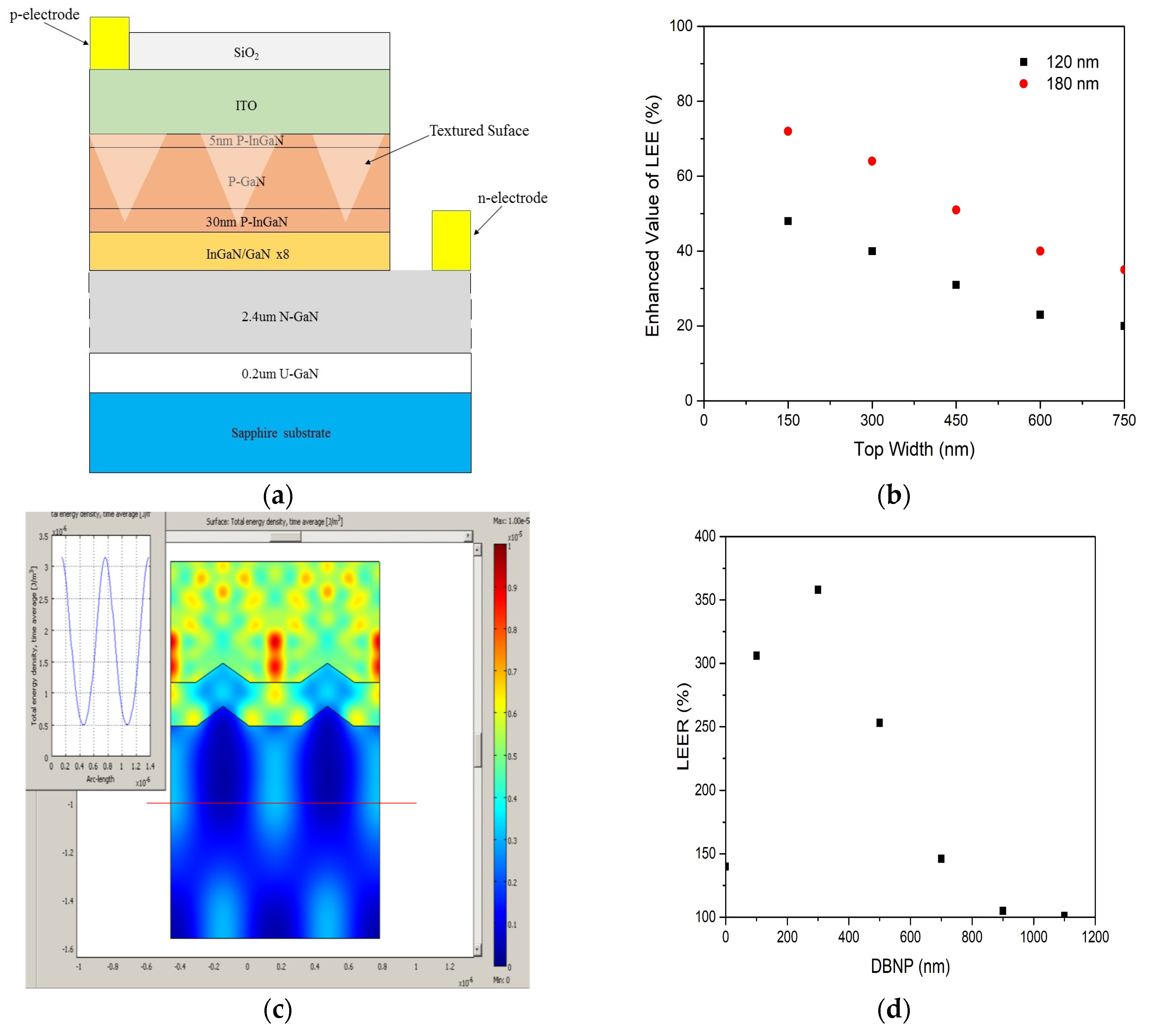
3.1. Simulation of LEE

To obtain an understanding of how to enhance LED output power, it is necessary to examine the relationship between the light extraction efficiency and the surface texture, as indicated by FEM. Figure 1a shows a schematic diagram of the LED structure with the surface texture. As can be seen, the arrangement of the IHPS on the surface of LED0 is continuous and uniform. The surface textures on LED0 with the various top widths are very much like those reported in [13,17]. Figure 1b shows the enhancement in values of the LEE for LED0s, according to the FEM simulation, with various top widths at depths of 180 nm and 120 nm, when the p-GaN layer thickness is 200 nm. For all LED0s, there is a gradual change in the refractive index. Therefore, the LEE of all LED0 samples is more than that of the CLED, and the smaller the top width and larger the depth of the IHPS, the more the LEE.
In this study, the top width and depth of the IHPS were set to 300 nm and 180 nm, respectively, in the FEM simulations. The LED emitting wavelength was set to 460 nm. The CLED did not have the IHPS structure. The thickness of the p-GaN layer for all LEDs was 200 nm. For all LEDs except the CLED and LED0, a ZrO2 thin film was coated on the surface of the IHPS to prevent short circuits and electrical burns. As a consequence, there was little or no current flow beneath the IHPS. The distances between two neighboring IHPS patterns (DBNP) on the surface of LED0, LED1, LED3, LED5, LED7, LED9, LED11 were fixed at 0 nm, 100 nm, 300 nm, 500 nm, 700 nm, 900 nm, 1100 nm, respectively. An electric field is emitted from quantum wells in the InGaN/GaN active region. The FEM simulated output power intensity (PI) distribution (PID) was obtained under the following condition, that is, the same initial emission power (PIinitial) density in the InGaN/GaN active region. The PI rate is PIair/PIinitial, where PIair indicates the PI in air. The light extraction efficiency ratio (LEER) is the ratio of the PIair for the LED with the IHPS (IHP-LED) to that of the CLED. The power intensity distribution as simulated by FEM for LED3 is shown in Figure 1c. The power intensity value distribution at the red line in Figure 1c is also clearly indicated. The light on the surface without the IHPS is assumed to be like that of a small lamp perpendicular to the surface. In other words, the angle of the light is affected by the IHPS. A reduction in the incidence angle at the interface between the GaN and ITO layers should enhance the light extraction efficiency. Figure 1d shows the effect of the DBNP on the LEER, as obtained in the simulation at the same input current density. The light is reflected at a high emission angle by the IHPS, meaning that the LEE of the IHP-LEDs will be more than that of the CLED. The decrease in the reflected light leads to an increase in the light extraction efficiency. The simulation results showed an improvement in the LEER of more than 250%, with DBNP sizes ranging from 100 nm to 500 nm. The best LEER of 358% was obtained when the DBNP size was 300 nm.

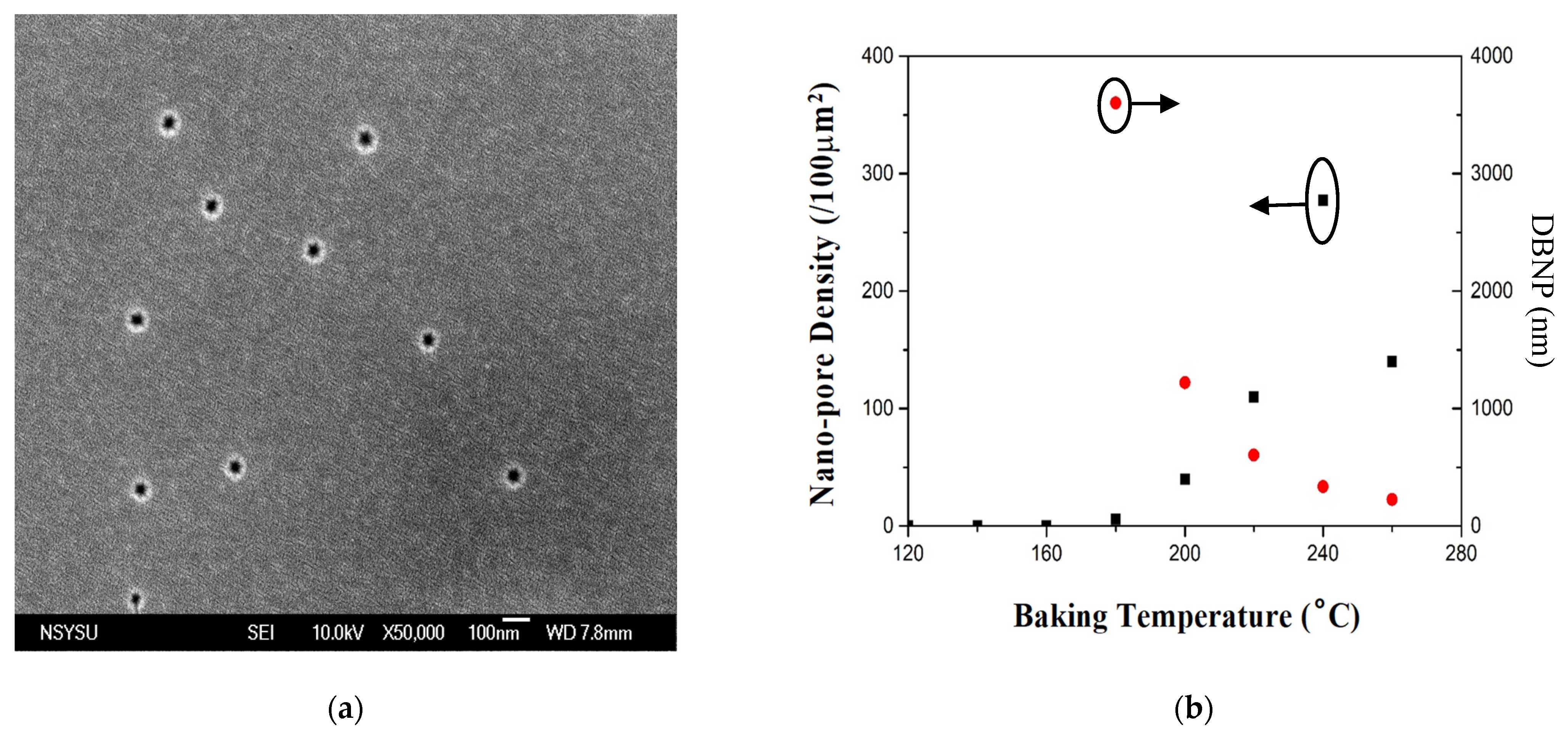
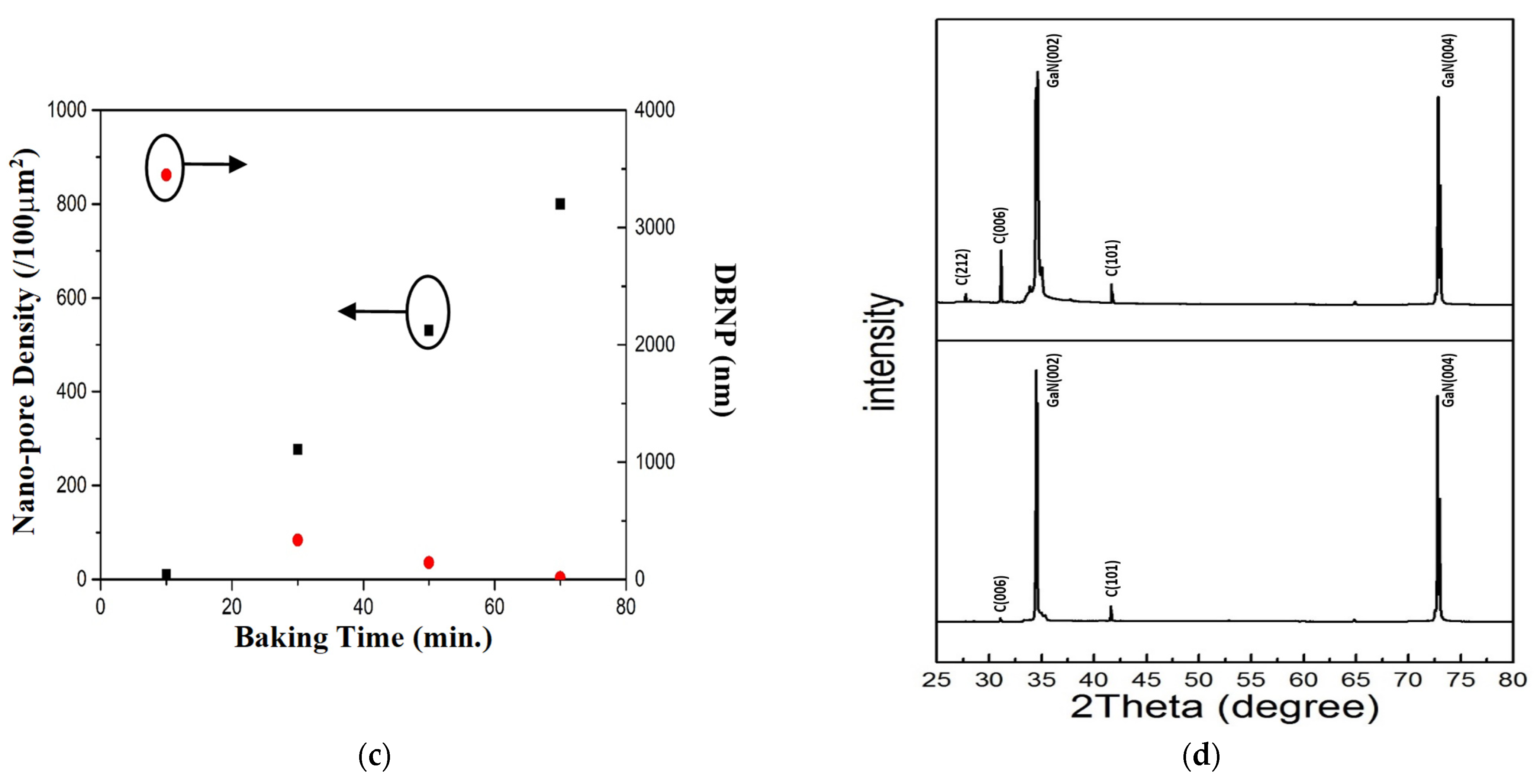
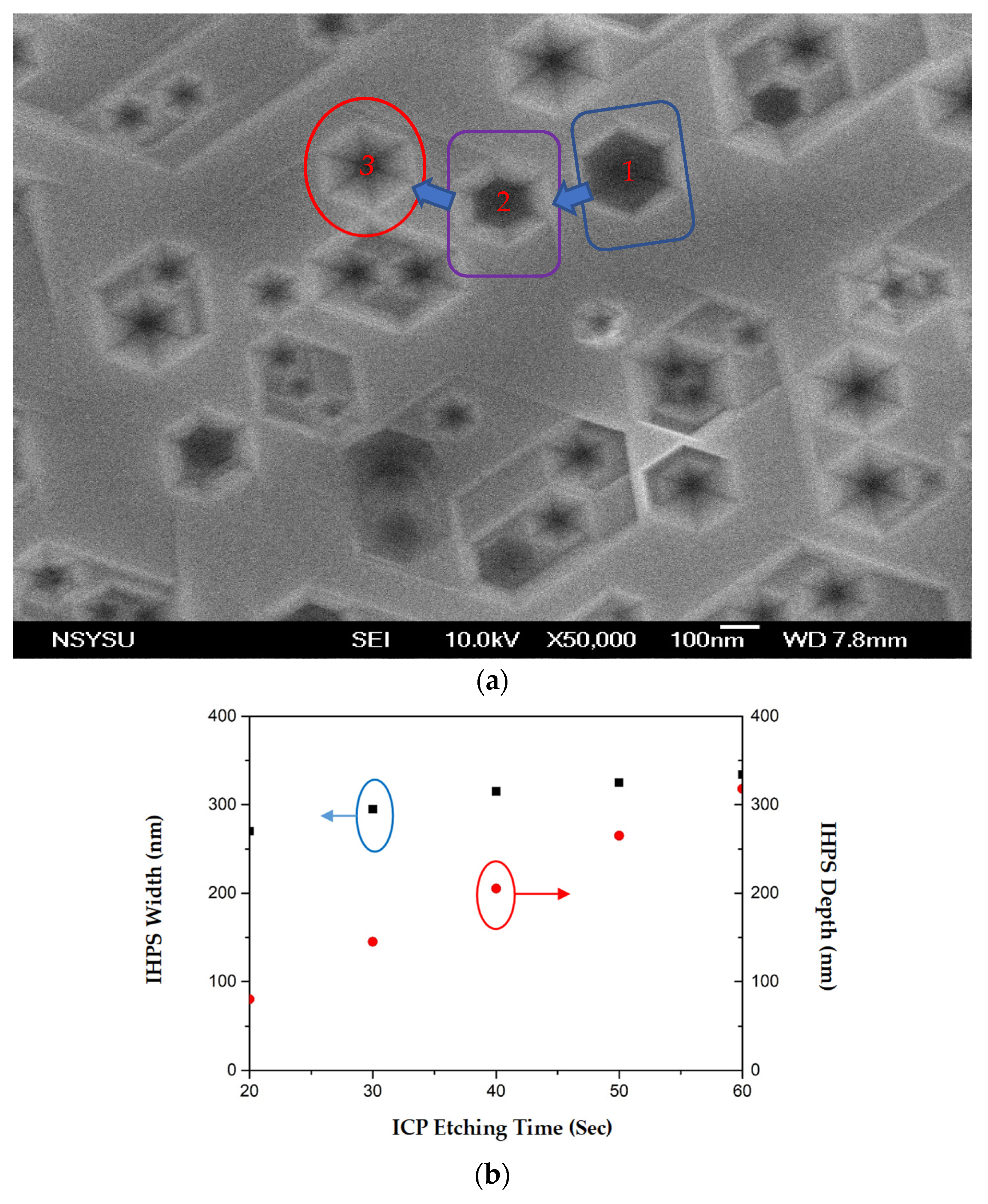
3.2. Fabrication of IHPS LED

The smaller the top width of the IHPS, the larger the LEE. However, when the pore structure in the photoresist is bigger, the top width of the IHPS will be wider after ICP etching. Therefore, a nano-pore structure in the photoresist is required for the fabrication of IHPS with a smaller top width. No pore structure on the photoresist and no IHPS on the surface of the p-GaN layer were found in LEDs produced using the standard factory processes (i.e., baking of the photoresist at 120 °C and the ICP process). It is not easy to etch the surface of the p-GaN layer to obtain IHPs with small top widths and large depths. However, since baking changes the structure of the photoresist, the effect of the baking temperature and time on the density of the nano-pore structure needs to be investigated. Figure 2a shows a top view FESEM image of the photoresist on the p-GaN layer that was baked at 220 °C and etched using ICP-RIE. Figure 2b shows the nano-pore density and DBNP in the photoresist in samples baked at various temperatures for a time of 30 min and then etched by the ICP process. Figure 2c shows the nano-pore density and DBNP in the photoresist in specimens baked at a temperature of 240 °C for various times and then etched by the ICP process. It can be clearly seen that a nano-pore structure formed in the resist without a mask after baking at a temperature of more than 160 °C and ICP etching. Clearly, except when the baking temperature exceeded 260 °C (when the photoresist was broken), the higher the baking temperature, the greater the number of nano-pore structures, although the diameter of the nano-pore structures only increased from ~40 nm to less than 50 nm. Figure 2d shows XRD patterns of the photoresist on samples baked at 160 °C and 240 °C. The peaks at C(212) and C(006) are smaller at 240 °C than at 160 °C. This indicates that the composition of the photoresist within the nano-pore structures is likely comprised of C(212) and C(006) before baking. Thus, the baking temperature affects the composition of the photoresist.
In order to achieve high LEE enhancement, as illustrated in Figure 1b,d, IHPS with top widths of less than 0.4 μm and depths deeper than 150 nm are required. The effect of the ICP etching time on changes in the width and depth of the IHPS was investigated next.
Figure 3a shows top-view FESEM images illustrating the procedure for the formation of the IHPS on the top surface of GaN-based LEDs: steps 1, 2 and 3. It was found that with a gradual increase in the ICP etching time, the width of the IHPS first increased, and then the depth of the IHPS in the vertical plane deepened. Furthermore, the etched patterns are hexagonal because the etching speed corresponds to the crystalline orientation in the p-GaN layer. Figure 3b shows the effect of the ICP etching time on the changes in the width and depth of` the IHPS on the surface of p-GaN. The longer the etching time is, the deeper the depth. However, there is little variation in the top widths of the IHPS. This anisotropic etching occurs because the Cl plasma ions prefer to etch the p-GaN layer in the vertical direction [26,27,28,29], so the nano-pore structure in the baked photoresist acted as an etching mask to restrict the area etched by the Cl plasma ions. A cross-sectional FESEM image of the surface morphology of the p-GaN layer after being baked at 240 °C and etched is shown in Figure 4a. An IHPS with a top width of 290 nm, a depth of 170 nm and a DBNP of 180 nm on the LED surface was fabricated. The IHPS LED had an enhanced light extraction efficiency of 305%, as shown in Figure 4b. Therefore, as noted above, by controlling the baking temperature and time and the etching time, IHPS with small top widths and large depths can be easily fabricated to produce desirable high surface-density textures for an IHP-LED.

4. Conclusions

The relationship between the light extraction efficiency and the surface texture (which includes the width and depth of the IHPS and the distance between two neighboring IHPS patterns) has been discussed. The LEE of the LED is completely dependent on the surface texture. IHPS with smaller top widths and larger depths will enhance the LEE. Light extraction efficiency ratios of more than 250% were obtained when the DBNP was between 100 nm and 500 nm in size. In particular, an optimal LEER of 358% was obtained when the DBNP was 300 nm. Nano-pore structures in the photoresist (used as the etching mask) could be easily fabricated by controlling the processing conditions (i.e., the baking temperature and time, and the ICP etching time) for the fabrication of surface textures with various IHPS densities for enhancement of the light extraction efficiency of the LED. When the process conditions were controlled (a baking temperature of 240 °C, a baking time of 30 min, and an ICP etching time of 60 s) it was found that the composition of the photoresist within the nano-pore structures comprised C(212) and C(006). The results showed that the baking temperature affects the composition of the photoresist. Nano-pore structures with diameters of less than 50 nm in the photoresist etching mask produced IHPS with a width of 290 nm and depth of 170 nm, and a DBNP of 190 nm on the LED surface, and an enhanced light extraction efficiency of 305% was obtained. The results show this method to be capable of forming IHP-LEDs with enhanced light extraction efficiency.
The results indicate the ICP etching can be used to produce IHPS patterns which lead to improved luminous intensity of the LED, as long as the nano-pores fabricated in the photoresist have diameters of less than 50 nm using any processing technology. Furthermore, this technology could be used to improve the yield of the future micro-LED production.

Funding

This research received no external funding.

Acknowledgments

This research was supported by the National Science Council of Taiwan under contract no. MOST 104-2221-E-327-028 and MOST 109-2637-E-992-004. Thanks to Master Shih-Hao Cheng for helping to etch the LED chip and measure the luminous intensity. Additionally, thanks to Master Bo-Hao Chen for helping to simulate the luminous intensity.

Conflicts of Interest

The author declares no conflict of interest.

References

  1. Ge, M.; Li, Y.; Zhu, Y.; Wang, M. Investigation on Light Extraction Behavior of Surface Plasmon-Coupled Deep-Ultraviolet LED in Different Emission Directions. Crystals 2022, 12, 82. [Google Scholar] [CrossRef]
  2. Huang, C.-H.; Kang, C.-Y.; Chang, S.-H.; Lin, C.-H.; Lin, C.-Y.; Wu, T.; Sher, C.-W.; Lin, C.-C.; Lee, P.-T.; Kuo, H.-C. Ultra-High Light Extraction Efficiency and Ultra-Thin Mini-LED Solution by Freeform Surface Chip Scale Package Array. Crystals 2019, 9, 202. [Google Scholar] [CrossRef] [Green Version]
  3. Pai, Y.-M.; Lin, C.-H.; Lee, C.-F.; Lin, C.-P.; Chen, C.-H.; Kuo, H.-C.; Ye, Z.-T. Enhancing the Light-Extraction Efficiency of AlGaN-Based Deep-Ultraviolet Light-Emitting Diodes by Optimizing the Diameter and Tilt of the Aluminum Sidewall. Crystals 2018, 8, 420. [Google Scholar] [CrossRef] [Green Version]
  4. Anwar, A.R.; Sajjad, M.T.; Johar, M.A.; Hernández-Gutiérrez, C.A.; Usman, M.; Łepkowski, S.P. Recent Progress in Micro-LED-Based Display Technologies. Laser Photonics Rev. 2022, 16, 2100427. [Google Scholar] [CrossRef]
  5. Yu, H.; Memon, M.H.; Jia, H.; Zhang, H.; Tian, M.; Fang, S.; Wang, D.; Kang, Y.; Xiao, S.; Long, S.; et al. A 10 × 10 deep ultraviolet light-emitting micro-LED array. J. Semicond. 2022, 43, 062801. [Google Scholar] [CrossRef]
  6. Solís-Cisneros, H.I.; Hu, Y.; Camas-Anzueto, J.L.; Grajales-Coutiño, R.; Anwar, A.-R.; Martínez-Revuelta, R.; Hernández-de-León, H.R.; Hernández-Gutiérrez, C.A. Theoretical and Computational Analysis of a Wurtzite-AlGaN DUV-LED to Mitigate Quantum-Confined Stark Effect with a Zincblende Comparison Considering Mg- and Be-Doping. Nanomaterials 2022, 12, 4347. [Google Scholar] [CrossRef]
  7. Na, S.-I.; Ha, G.-Y.; Han, D.-S.; Kim, S.-S.; Kim, J.-Y.; Lim, J.-H.; Kim, D.-J.; Min, K.-I.; Park, S.-J. Selective Wet Etching of p-GaN for Efficient GaN-Based Light-Emitting Diodes. IEEE Photon. Tech. Lett. 2006, 18, 1512–1514. [Google Scholar]
  8. Fujii, T.; David, A.; Gao, Y.; Iza, M.; DenBaars, S.; Hu, E.; Weisbuch, C.; Nakamura, S. Cone-Shaped Surface GaN-Based Light-Emitting Diodes. Phys. Stat. Sol. C 2005, 2, 2836–2840. [Google Scholar] [CrossRef]
  9. Nedy, J.G.; Young, N.; Kelchner, K.; Hu, Y.; Farrell, R.; Nakamura, S.; DenBaars, S.; Weisbuch, C.; Speck, J. Low Damage Dry Etch for III-Nitride Light Emitters. Semicond. Sci. Technol. 2015, 30, 085019. [Google Scholar] [CrossRef]
  10. Kim, H.; Cho, J.; Lee, J.W.; Yoon, S.; Kim, H.; Sone, C.; Park, Y. Enhanced Light Extraction of GaN-Based Light-Emitting Diodes by Using Textured-Type GaN Layers. Appl. Phys. Lett. 2007, 90, 161110. [Google Scholar] [CrossRef]
  11. Wierer, J.J.; Aurelien, D.; Mischa, M. III-Nitride Photonic-Crystal Light-Emitting Diodes with High Extraction Efficiency. Nat. Photon. 2009, 3, 163–169. [Google Scholar] [CrossRef]
  12. Koike, K.; Lee, S.; Cho, S.R.; Park, J.; Lee, H.; Ha, J.-S.; Hong, S.-K.; Lee, H.-Y.; Cho, M.-W.; Yao, T. Improvement of Light Extraction Efficiency and Reduction of Leakage Current in GaN-Based LED via V-Pit Formation. IEEE Photon. Tech. Lett. 2012, 24, 449–451. [Google Scholar] [CrossRef]
  13. Lai, F.-I.; Hsieh, Y.-L.; Lin, W.-T. Enhancement in the Extraction Efficiency and Resisting Electrostatic Discharge Ability of GaN-Based Light Emitting Diode by Naturally Grown Textured Surface. Diam. Rel. Mater. 2011, 20, 770–773. [Google Scholar] [CrossRef]
  14. Yeh, Y.-H.; Sheu, J.-K.; Lee, M.-L.; Yen, W.-Y.; Peng, L.-C.; Yeh, C.-Y.; Liao, P.-H.; Chen, P.-C.; Lai, W.-C. Vertical GaN-Based LEDs With Naturally Textured Surface Formed by Patterned Sapphire Substrate With Self-Assembled Ag Nanodots as Etching Mask. IEEE Trans. Electr. Dev. 2015, 62, 2919–2923. [Google Scholar] [CrossRef]
  15. Wang, M.-S.; Yang, L.; Huang, X.-J. Strong Enhancement in Light Output of GaN-Based LEDs with Graded-Refractive-Index ITO Deposited on Textured V-Shaped Pits. IEEE Electr. Dev. Lett. 2014, 35, 464–466. [Google Scholar] [CrossRef] [Green Version]
  16. Yoo, Y.-S.; Song, H.; Jang, M.-H.; Lee, S.-W.; Cho, Y.-H. Electrically driven, highly efcient three-dimensional GaN-based light emitting diodes fabricated by selfaligned twofold epitaxial lateral overgrowth. Sci. Rep. 2017, 7, 9663. [Google Scholar] [CrossRef] [PubMed] [Green Version]
  17. Chen, X.; Kong, F.; Li, K.; Ding, Q.; Zhang, M.; Li, W. Study of Light Extraction Efficiency of Flip-Chip GaN-Based LEDs with Different Periodic Arrays. Opt. Commun. 2014, 314, 90–96. [Google Scholar] [CrossRef]
  18. Boughrara, N.; Benzarti, Z.; Khalfallah, A.; Oliveira, J.; Evaristo, M.; Cavaleiro, A. Thickness-dependent physical and nanomechanical properties of AlxGa1−xN thin films. Mater. Sci. Semicond. Process. 2022, 151, 107023. [Google Scholar] [CrossRef]
  19. Benzarti, Z.; Sekrafi, T.; Bougrioua, Z.; Khalfallah, A.; El Jani, B. Effect of SiN Treatment on Optical Properties of InxGa1xN/GaN MQW Blue LEDs. J. Electron. Mater. 2017, 46, 4312–4320. [Google Scholar] [CrossRef]
  20. Lai, F.-D.; Li, W.-Y. Design, Fabrication and Analysis for Al2O3/Ti/Al2O3/Ti Color Solar Selective Absorbers for Building Applications. Coatings 2022, 12, 521. [Google Scholar] [CrossRef]
  21. Lai, F.-D. Optical Property Analysis Contour Map and Fabrication of SiO2/Cr SiO2/Cr Multilayer Films for High Photo Thermal Conversion Efficiency. Integr. Ferroelectr. 2020, 210, 64–72. [Google Scholar] [CrossRef]
  22. Lai, F.-D.; Li, W.-Y. SiO2/Ti/SiO2 Three-layer Films Used as Solar Selective Absorber Layer in Heat Energy Collector. Integr. Ferroelectr. 2013, 145, 158–164. [Google Scholar] [CrossRef]
  23. Lai, F.-D.; Li, W.-Y.; Huang, C.Y.; Hua, J.-M.; Chang, K.-C.; Cho, T.-P.; Tsai, Y.-H. Optical Properties and Enhanced Photothermal Conversion Efficiency of SiO2/a-DLC Selective Absorber Films for A Solar Energy Collector Fabricated by Unbalance Sputter. Phys. Procedia 2012, 32, 206–213. [Google Scholar] [CrossRef]
  24. Lai, F.-D.; Li, W.-Y.; Chang, K.-C.; Wang, Y.-Z.; Chi, P.-L.; Su, J.-Y. Optical properties, Optimized Design and Fabrication of SiO2/W/SiO2 films for Solar Selective Absorber. Integr. Ferroelectr. 2012, 137, 77–84. [Google Scholar] [CrossRef]
  25. Lai, F.-D. Fabrication of T Molds with Nano-scale Features for Nanoimprint Lithography Applications. Integr. Ferroelectr. 2014, 152, 36–42. [Google Scholar] [CrossRef]
  26. Lai, F.-D. Nano-image Profiles Transferred by Near Field Phase-Shifting Lithography Precisely Simulated by Finite Element Method and Fabricated. Appl. Surf. Sci. 2012, 258, 2113–2116. [Google Scholar] [CrossRef]
  27. Zhuang, D.; Edgar, J. Wet Etching of GaN, AlN, and SiC: A Review. Mater. Sci. Eng. R 2005, 48, 1–46. [Google Scholar] [CrossRef]
  28. Weyher, J.; Brown, P.; Rouvière, J.; Wosinski, T.; Zauner, A.; Grzegory, I. Recent Advances in Defect-Selective Etching of GaN. J. Crys. Grow. 2000, 210, 151–156. [Google Scholar] [CrossRef]
  29. Shintani, A.; Minagawa, S. Kinetics of the Epitaxial Growth of GaN Using Ga, HCl and NH3. J. Electrochem. Soc. 1976, 123, 706–713. [Google Scholar] [CrossRef]
Figure 1. (a) Schematic diagram of a LED structure with textured surface. (b) Enhanced LEE values for LED0s, as simulated by FEM, with various top widths at depths of 180 nm and 120 nm when the p-GaN layer thickness is 300 nm. (c) Power intensity distribution as simulated by FEM for LED3. The power intensity value distribution at the red line is also clearly shown. (d) Effect of DBNP on LEER for LED3.
Crystals 13 00491 g001
Figure 2. (a) Top view FESEM image of the photoresist on the p-GaN layer after being baked at 200 °C and etched using ICP-RIE. (b) The nano-pore density and DBNP in the photoresist baked at various temperatures for 30 min and then etched by the ICP process. (c) The nano-pore density and DBNP in the photoresist baked at a temperature of 240 °C for various times and then etched by ICP the process. (d) X-ray diffraction patterns of the photoresist on samples baked at 160 °C and 240 °C.
Crystals 13 00491 g002aCrystals 13 00491 g002b
Figure 3. (a) Top-view FESEM images showing the procedure for the formation of the IHPS on the top surface of GaN-based LEDs: steps 1, 2 and 3. (b) Effect of the ICP etching time on changes in the width and depth of` the IHPS on the surface of p-GaN.
Crystals 13 00491 g003
Figure 4. (a) Cross-sectional top-view FESEM image showing the surface morphology of the p-GaN layer after being baked at 240 °C and etched. (b) Power intensities of the common LED (CLED) and the IHPS LED.
Crystals 13 00491 g004
Disclaimer/Publisher’s Note: The statements, opinions and data contained in all publications are solely those of the individual author(s) and contributor(s) and not of MDPI and/or the editor(s). MDPI and/or the editor(s) disclaim responsibility for any injury to people or property resulting from any ideas, methods, instructions or products referred to in the content.

