Abstract
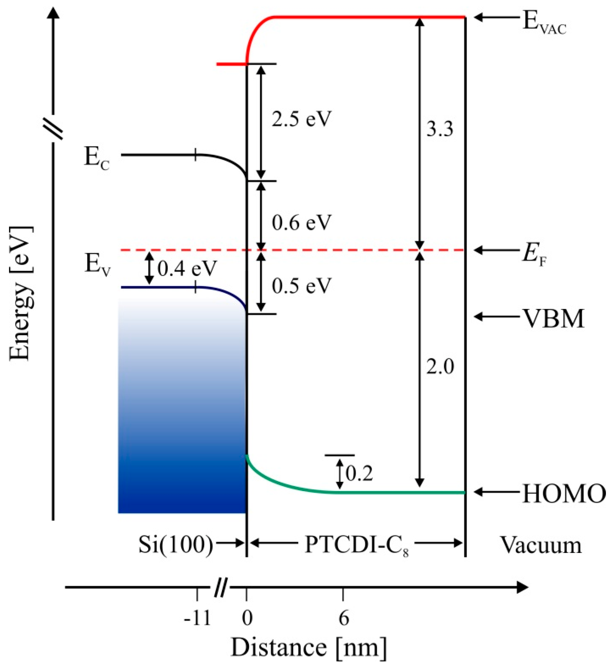
PTCDI-C8 molecules are vapor-deposited onto reconstructed Si(100)—(2 × 1) surface under ultra-high vacuum. X-ray photoelectron spectra reveal a bond formation between oxygen atoms of the molecules’ carboxylic groups and Si dangling bonds of the substrate. Following PTCDI—C8 film growth, ultraviolet photoelectron spectra show a drop in the HOMO level with respect to the Fermi level from 1.8 eV to 2.0 eV and a monotonic work function increase from 2.5 eV up to 3.3 eV. For a film thickness of 6.0 nm, a difference of 1.5 eV between the HOMO level of the film and the valence band maximum of the substrate is accomplished.
1. Introduction
The functionalization of inorganic semiconductors by direct bonding of organic molecules to the surface is a fast-growing area of research, due to a wide range of applications of such systems in optoelectronic devices [1,2,3,4]. Simultaneously, there is also great interest in these interfaces regarding the fundamental science. Therein, the deposition of molecular thin films usually proceeds onto well-defined inorganic surfaces, and their characterizations or modifications are performed in situ. Such conditions allow the indication of interactions between components and their influence on system properties. Moreover, the possibility of interface modifications with atomic precision is achieved. For instance, adsorbed organic molecules can play a role of precursors for the synthesis of (nano)graphenes on semiconducting surfaces by scanning tunneling microscope (STM) tip-induced dehydrogenation [5].
It is well-documented that the electronic properties of the junction between an organic film and an inorganic substrate depend on the chemical interaction of molecules constituting the film with the substrate surface, as well as the morphology of the deposited film [6,7,8,9,10]. As was shown on conventional IV and III-V semiconductors, the chemical interactions can be tuned by changing the molecular chemical composition, for example, metal atoms coordinated by complex compounds such as phthalocyanines or tris(8-hydroxyquinoline) [10,11]. At the interface, the thin-film morphology results from the interplay between molecule–substrate and intermolecular interactions. Si and Ge possess strongly interacting surfaces with high densities of reactive dangling bonds. As a result, organic molecules are generally covalently bonded to these surfaces and the formation of chemical bonds limits their diffusion and, as a consequence, self-ordering, as was shown for perylene derivatives [12,13,14]. The interfacial interactions between organic molecules and inorganic semiconductors impact the electronic structure of formed systems due to an electron transfer at the phase boundary. This results in offsets of occupied and un-occupied bands of systems.
A series of available perylene and its derivatives were studied with respect to their application in various (opto)electronic and photovoltaic devices as well as electrocatalysts [15,16,17]. Among these derivatives are N,N′-dialkyl-3,4,9,10-perylene-tetracarboxylic-diimides (PTCDI-Cn), for which the base compound is PTCDI (C24H10N2O4) with the alkyl chains attached to two nitrogen atoms. By varying the length of alkyl chains, the distance between adsorbates in bimolecular systems can be controlled and, thus, influences the power conversion efficiencies of organic photovoltaics [18]. The electronic structure of thin PTCDI films on semiconducting surfaces has been previously investigated, using photoelectron spectroscopy methods, for Si(111) [19], TiO2 [20,21], Ag/Si(111)-√3 × √3 [22] and Sn/Si(111)-2√3 × 2√3 [23]. The chemical interactions and band alignments for PTCDI-Cn in contact with inorganic surfaces mainly concern non-conventional semiconductors, such as MoS2 (PTCDI-C4) [24] or lead halide perovskite (PTCDI-C5) [25].
In this study, we focus on PTCDI-C8 (C40H42N2O4), a stable n-type semiconductor that has applications in organic field-effect transistors [26,27], solar cells [28] and photodetectors [29,30]. In our earlier work, we have shown that the morphology of the PTCDI-C8 layer on the Si(100)-2 × 1 surface is determined by the strong molecule–substrate interaction, and found that the molecules are bound to the surface through oxygen from the carboxylic group [14]. Such strong adsorbate–Si(100) interactions result in a lack of ordered structure formation by PTCDI-C8 molecules as was shown for sub-to-multi-layer regimes by STM [14]. In contrast to the Si(100)-2 × 1 surface, the well-ordered domains of PTCDI-C8 were found on Si(110)-16 × 2 and Si with native oxide (SiO2) surfaces [31,32,33]. Due to presence of Si–O bonding, the SiO2/Si surface is much less reactive in comparison to the non-oxidized one, which allows for the self-ordering of molecules. In the case of the Si(110)-16 × 2 surface, the charge transfer from the surface to the molecules occurs and results in the self-organization of negatively charged PTCDI-C8 [31].
The variable degree of PTCDI-C8 ordering observed by us on Si(110)-16 × 2 vs. Si(100)-2 × 1, described in Refs. [14,31], strongly suggests that the interfacial energy level alignments are different in both systems. Therefore, in this work, we present a detailed analysis of the chemical state and changes occurring in the electronic structure of the PTCDI-C8/Si(100) interface during its formation. Herein, the electronic structures are probed by both X-ray and UV photoelectron spectroscopies (XPS and UPS). The combination of these technique allows us to confirm Si–O bond formation and explain the tendency of PTCDI-C8 molecules toward agglomeration, as described in a previous work.
2. Materials and Methods
Prior to placing p-Si(100) substrates (B-doped, Na~1018 cm−3) into an ultra-high vacuum (UHV) chamber, samples were chemically cleaned. Next, they were degassed in situ at 500 °C for 12 h, then repeatedly flashed at 1350–1400 °C under UHV to prepare the initial surface. Chemical analysis confirmed the presence of small amounts of contaminants on the surface, i.e., about 13% carbon and about 2% oxygen. Using LEED, the (2 × 1) reconstruction of the substrate surface was confirmed. PTCDI-C8 molecules (Sigma-Aldrich, St. Louis, MO, USA) were deposited by physical vapor deposition (PVD) on the initial surface kept at room temperature (RT). The evaporation rate was 0.6 nm/min and was calibrated by means of a quartz crystal resonator as in previous works [34,35]. The film growth and its characterization were performed step by step.
The samples were characterized using XPS equipped with a Mg Kα radiation source (1253.6 eV) and UPS with the He I line (21.2 eV). Photoelectrons were collected with a hemispherical electron energy analyzer (Phoibos 100, SPECS) with 0.1 eV and 0.025 eV steps for XPS and UPS, respectively. Photoelectrons were collected with pass energy values of 10 eV and 2 eV for XPS and UPS measurements, respectively. The analyzer entrance was normal to the substrate surface during experiments. All binding energies were relative to the Fermi level of the analyzer, which was determined on a clean reference Au sample. No charging effects were observed during measurements and no binding energy corrections were used in this study.
3. Results and Discussion
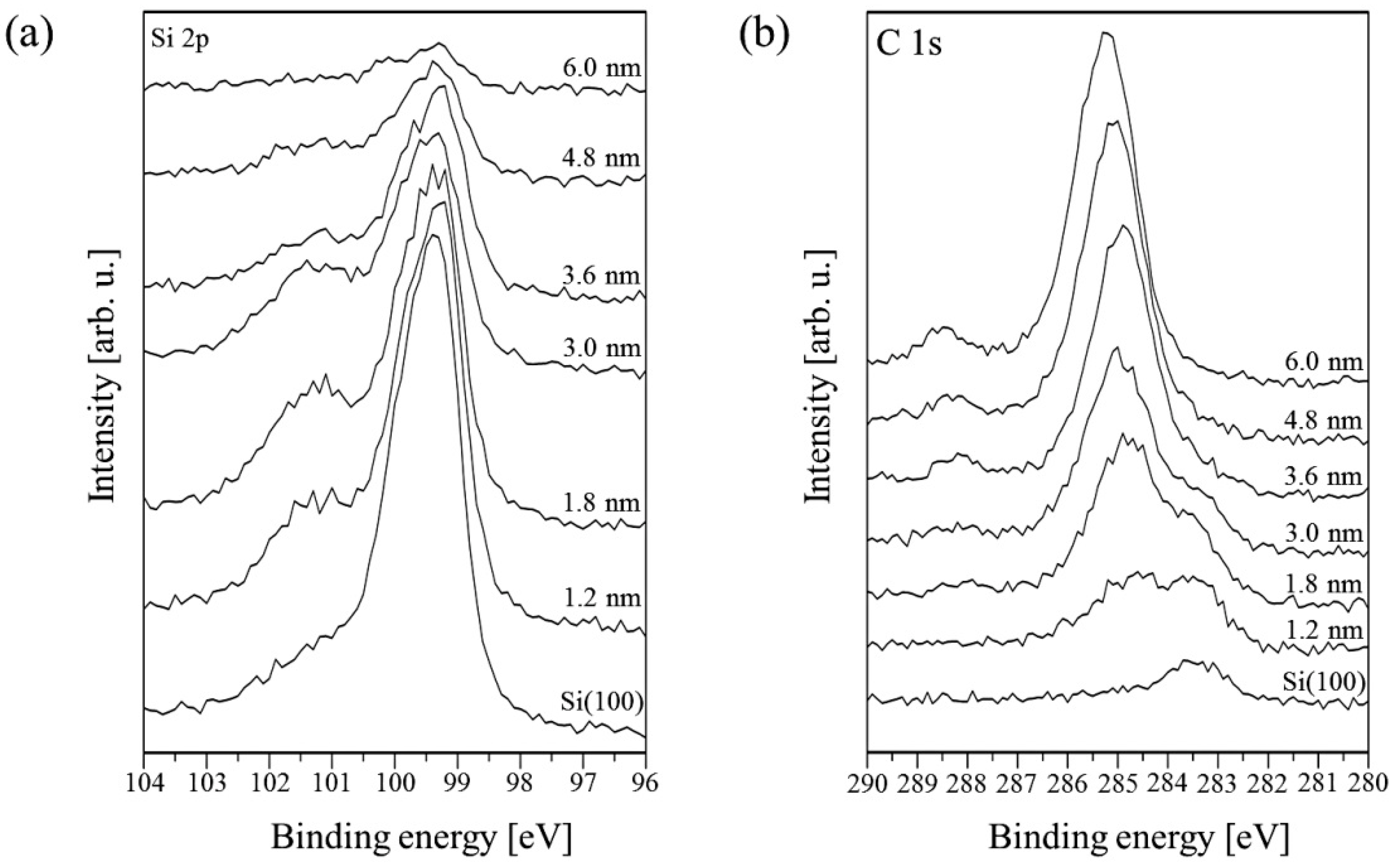
Information about chemical composition and interactions between PTCDI-C8 molecules and the substrate has been acquired from XPS data. Four core-level lines have been analyzed: Si 2p, C 1s, O 1s and N 1s. Meaningful changes occur in the Si 2p and C 1s regions. In Figure 1, the XPS spectra of these energy regions collected for PTCDI-C8 films of various thickness values ranging from 0 up to 6 nm are compared. Before PTCDI-C8 deposition, the Si 2p core-level line consists of four peaks. They are the Si 2p3⁄2 and Si 2p1⁄2 doublet, for which the first state is overlapped with the Si–C bond (from carbon contaminating the substrate surface). An additional component with a maximum at 101.2 eV is assigned to Si–O bonds. The last component with the lowest binding energy corresponds to the surface Si. It disappears completely when the film thickness exceeds 3.0 nm.

Figure 1.
Evolution of the XPS spectra as a function of the PTCDI-C8/Si(100) film thickness in the energy regions of (a) the Si 2p and (b) C 1s lines.
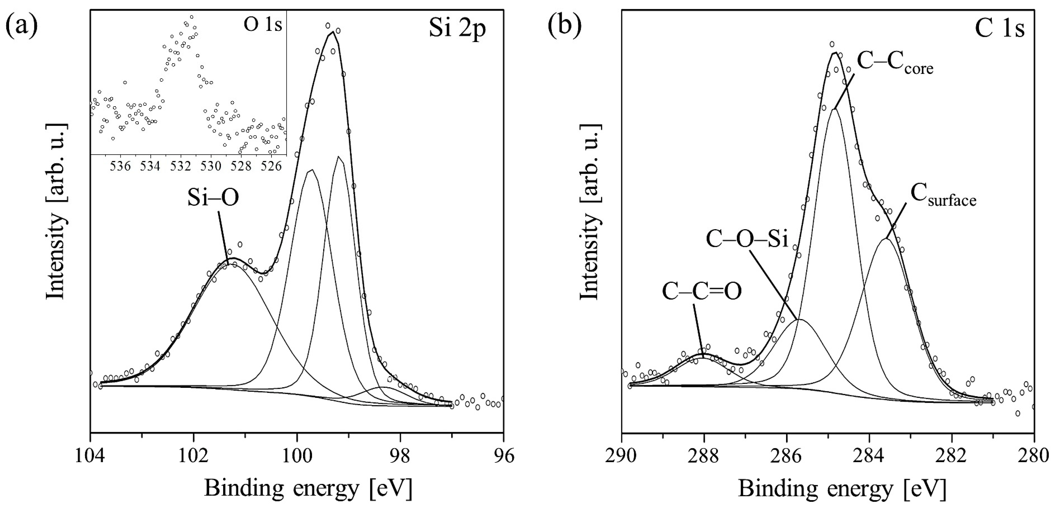
A detailed analysis of the Si 2p line for an example PTCDI-C8 layer with a thickness of 1.8 nm, on which all components are visible, is shown in Figure 2a. It is clearly evident that the ratio of the doublet components is disturbed. This is due to the overlapping of the Si 2p1/2 state with the Si–C bond component.

Figure 2.
Deconvolution of Si 2p (a) and C 1s (b) core-level lines measured for the PTCDI-C8/Si(100) film of average thickness equal to 1.8 nm. The inset on (a) shows the O 1s line of this film.
Following film growth, the intensity of the Si 2p line declines. Its shape changes due to intensity variations of the constituent peaks. Up to 3.0 nm, the Si–O peak increases, whereas the Si–Si doublet decreases. The increase in the Si–O peak in the film thickness range of 0–3.0 nm provides strong evidence for bond formation between oxygen atoms of the molecules’ carboxylic groups and Si dangling bonds. This means that the molecules chemically react with the surface even at RT. When the average thickness of the film reaches 3.0 nm, all components begin to shrink simultaneously. This indicates completion of the first molecular layer, which is in direct contact with the substrate. At this stage of PTCDI-C8 film growth, the Si–O bond formation is completed and further deposition equally attenuates all the components of the Si 2p line, i.e., the line disappears. Following film growth, the C 1s line changes its shape and its intensity increases due to the carbon present in molecules. An example of detailed analysis for a 1.8 nm thick film is shown in Figure 2b. The line is fitted by four components. The complex shape of the C 1s core-level line results not only from the complexity of the deposited molecules, but also from carbon contaminants present on the substrate surface prior to deposition. An adequate peak connected with these contaminations, visible at the lowest spectrum in Figure 1b, has its maximum at 283.4 eV. In Figure 2b, this peak is marked Csurface. Its height decreases simultaneously with the Si–C component of the Si 2p line during film growth. When the average film thickness oversteps 3.6 nm, it disappears completely, as is shown in Figure 1b. The second and highest peak in this stage of the film growth has a binding energy equal to 284.6 eV and is attributed to C–C bonds in the perylene core and alkyl chains of the molecule, and also C–H bonds. The third peak at 285.4 eV is a mixture of signals from C–N bonds of the molecule and C–O–Si bonds, which are formed between the substrate and the molecule. The peak at 288.1 eV represents the carboxylic groups of the molecules.
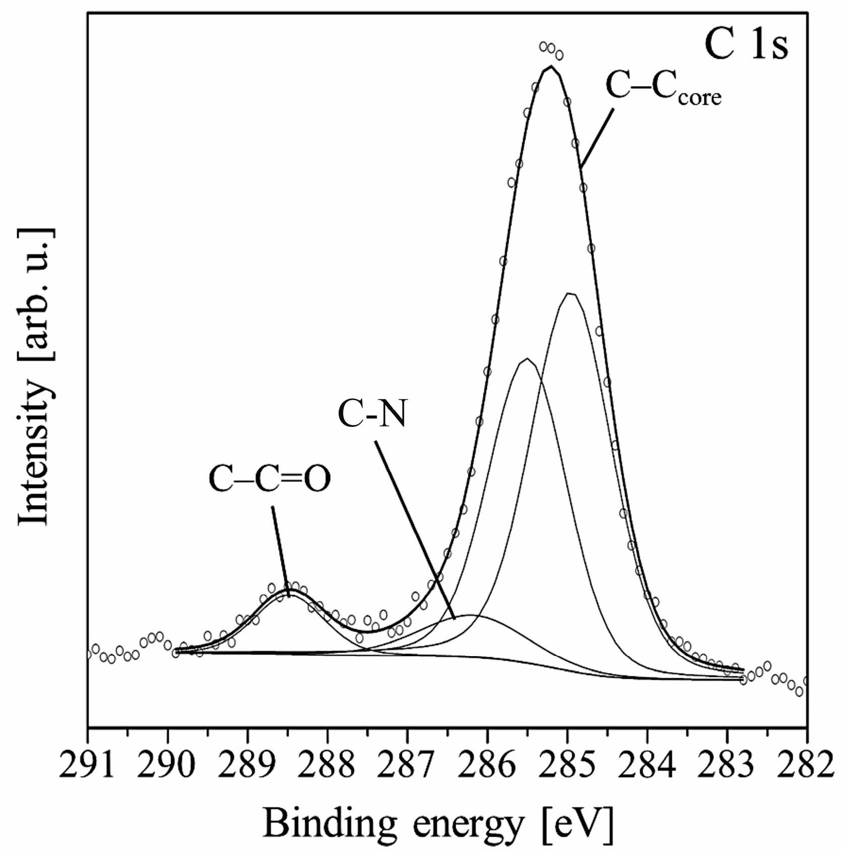
Further growth of the film shifts the position of the C 1s line maximum towards a higher binding energy. Finally, the shift equals 1.0 eV for the 6.0 nm thick film, for which the Si 2p signal almost completely disappears. At this stage of the growth, two peaks dominate the shape of the C 1s line. Both come from the carbon atoms of the molecule. The spectrum can be fitted by four components as is shown in Figure 3. The first two peaks correspond to C–C/C–H bonds in PTCDI and alkyl chains, respectively. The third peak at 286.5 eV is now mainly attributed to C–N bonds. The component with the highest binding energy of 288.6 eV comes from the bonds of carboxylic groups.

Figure 3.
Main components constituting the C 1s spectral line measured for the 6.0 nm thick PTCDI-C8/Si(100) film.
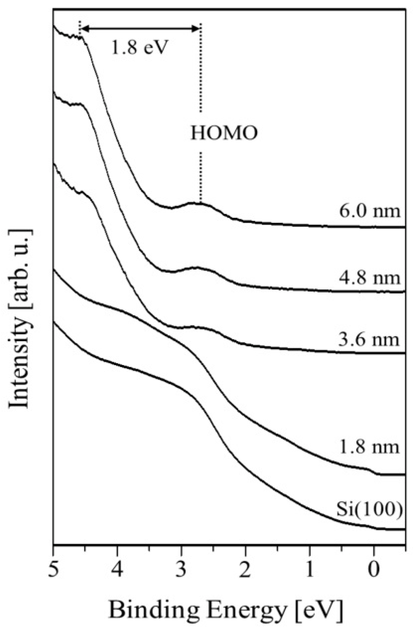
One can see in Figure 4 the UPS spectra obtained for various values of average PTCDI-C8 film thickness, showing that the valence band of the PTCDI-C8/Si(100) system evolves with the progression of film growth. The electron affinity χ of clean substrate calculated from equation χ = hν – W − Eg amounts to 2.5 eV, where: hv = 21.2 eV is the photon energy of He I; the spectrum width W is the energy difference between the valence band maximum (VBM) and the cutoff energy of photoemission (Ecutoff), equal to 17.6 eV; and Eg = 1.1 eV is the width of the Si band gap. The position of the VBM is found to be 0.5 eV above the Fermi level. The work function (WF) of the Si(100) surface, counted based on measured data, is equal to 3.1 eV and was determined using the following expression: ϕm = hν − Ecutoff.
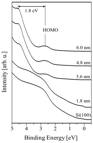
Figure 4.
The UPS spectra illustrating valence band evolution as a function of the PTCDI-C8/Si(100) film thickness.
The calculated Fermi level position at the bulk, based on the free electron model and Fermi–Dirac statistics, is located 0.4 eV above the VBM. Thus, the surface band bending at the vacuum/Si(100) interface calculated from the equation equals 0.1 eV. The bending comes from the electrostatic surface charging. Solving Poisson’s equation, we can obtain the space-charge region width , where ε = 11.7 is the dielectric constant of Si, ε0 represents the permittivity of free space and q is the elementary charge of an electron. The depletion layer width amounts to 11.0 nm. The HOMO level of the molecular layer becomes visible for the 1.8 nm thick film and is placed 1.3 eV above the VBM of the substrate. For this thickness, the WF achieves a value of 3.3 eV and remains constant for thicker films. An additional peak, located 1.8 eV above the HOMO level, appears at the UPS spectrum beginning at a film thickness of 3.0 nm. The origin of the peak is not clear, but according to other authors [8,9,10], it is associated with the π–π interactions between the cores of the molecules. As the film thickness increases, both peaks shift slightly towards higher energies—whereas the HOMO level holds its position 1.5 eV below the VBM, unchanged. The aforementioned electron band structure of the PTCDI-C8/Si(100) interface is schematically presented in Figure 5.
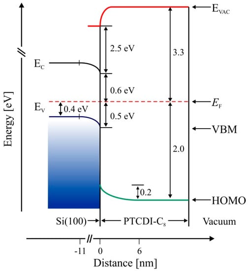
Figure 5.
Energy band diagram of the PTCDI-C8/Si(100) interface determined from UPS spectra. Left column corresponds to the bulk band structure and shows bending in the subsurface layer. Right side shows the properties of the interface.
Changes in shapes and shifts of individual peaks in the Si 2p, C 1s and O 1s spectral lines indicate that PTCDI-C8 molecules, which are in direct contact with the substrate, are bound to the surface through oxygen atoms of carboxylic groups. LEED patterns were not observed for the organic film; there was only a signal at the beginning of the PTCDI-C8 growth from the initial surface. This shows that there is no long-range order, i.e., there was no self-organization of the molecules at the Si(100) due to their strong chemical interaction with the initial surface. This is consistent with former studies of the first stages of PTCDI-C8 film growth on Si(100) with STM, wherein a close-range arrangement was similarly not observed [14]. The XPS results show that PTCDI-C8 molecules in direct contact with the substrate are adsorbed with the π-conjugated molecular rings parallel to the Si(100) surface. Similar adsorption geometry was found by STM for PTCDA on Ge(100) and Si(100) [12,13]. No chemical reaction was observed concerning alkyl chains. Thus, in the case of Si(100) surfaces, molecular engineering of alkyl chains pinning to the PTCDI core should not impact its self-organization on that surface, contrary to the energy structure.
The results of the aforementioned studies demonstrated that the molecules adsorbed randomly and their bond to the surface was strong enough to prevent self-organization of the adsorbate. As a consequence of strong molecule–substrate interaction, the film growth was amorphous [14]. In the case of PTCDI-C8 adsorption on Si(110), the same kind of binding through oxygen atoms of carboxylic groups, which should be of the same strength as on Si(100), did not stop self-organization [31]. The reason for this was a strong charge transfer from the surface to the molecule. DFT calculations showed that molecules directly adsorbed on the surface of the Si(110) substrate became negatively charged upon adsorption and that the charge transferred from the substrate to the adsorbed PTCDI-C8 molecules was equal to about 0.5 of the elementary charge carried by electrons. The DFT calculation have been confirmed by our yet unpublished UPS results. Strong Coulomb repulsion between charged molecules resulted in some of the sub-monomolecular films of PTCDI-C8 on Si(110) being very well-ordered. The energy band diagram of the PTCDI-C8/Si(100) interface, determined from UPS spectra and shown in Figure 5, clearly indicates that electron transfer from the surface to the molecule is impossible. The subsurface region of the substrate is negatively charged due to a depletion of the holes. The valence band maximum of the Si(100) surface is 0.5 eV below the Fermi level. When the molecular layer reaches an average thickness of about 3.0 nm, the WF achieves its final value of 3.3 eV.
4. Conclusions
We have presented results of XPS/UPS studies on early stages of interface formation of PTCDI-C8 on Si(100). We have found evidence for the strong interaction between molecules and substrate through oxygen atoms of PTCDI-C8, which prevents self-organization of the molecules. There was no evidence for the interaction of alkyl chains of the molecule with the surface. No LEED patterns were observed in PTCDI-C8 molecule films. The molecules are oriented such that the π-conjugated molecular rings are parallel to the Si(100) surface. The work function of amorphous PTCDI-C8 film deposited onto Si(100) surfaces equals 3.3 eV. The HOMO level position of the film drops from 1.3 eV to 1.5 eV below the Si VBM following the growth progress. An additional peak related to π–π intermolecular interactions inside the film is observed in the valence band when the film thickness exceeds 3.0 nm. The results obtained explain why electron transfer from the Si(100) surface onto the PTCDI-C8 molecule is impossible.
Author Contributions
Conceptualization, K.L. and M.G.; formal analysis, K.L. and M.G.; investigation, P.M.; writing—original draft preparation, K.L.; writing—review and editing, M.G., A.S., R.L. and A.C.; visualization, K.L. and M.G.; supervision, A.C. All authors have read and agreed to the published version of the manuscript.
Funding
This research received no external funding.
Data Availability Statement
Data available on request from the corresponding author.
Conflicts of Interest
The authors declare no conflict of interest.
References
- Liu, X.; Lee, E.K.; Kim, D.Y.; Yu, H.; Oh, J.H. Flexible Organic Phototransistor Array with Enhanced Responsivity via Metal–Ligand Charge Transfer. ACS Appl. Mater. Interfaces 2016, 8, 7291–7299. [Google Scholar] [CrossRef] [PubMed]
- Niederhausen, J.; Mazzio, K.A.; MacQueen, R.W. Inorganic–Organic Interfaces in Hybrid Solar Cells. Electron. Struct. 2021, 3, 033002. [Google Scholar] [CrossRef]
- Han, J.; Wang, F.; Han, S.; Deng, W.; Du, X.; Yu, H.; Gou, J.; Wang, Q.J.; Wang, J. Recent Progress in 2D Inorganic/Organic Charge Transfer Heterojunction Photodetectors. Adv. Funct. Mater. 2022, 32, 2205150. [Google Scholar] [CrossRef]
- Pei, K.; Zhai, T. Emerging 2D Organic-Inorganic Heterojunctions. Cell Rep. Phys. Sci. 2020, 1, 100166. [Google Scholar] [CrossRef]
- Zuzak, R.; Castro-Esteban, J.; Engelund, M.; Pérez, D.; Peña, D.; Godlewski, S. On-Surface Synthesis of Nanographenes and Graphene Nanoribbons on Titanium Dioxide. ACS Nano 2023, 17, 2580–2587. [Google Scholar] [CrossRef]
- Bent, S.F. Attaching Organic Layers to Semiconductor Surfaces. J. Phys. Chem. B 2002, 106, 2830–2842. [Google Scholar] [CrossRef]
- Bilić, A.; Reimers, J.R.; Hush, N.S. Functionalization of semiconductor surfaces by organic layers: Concerted cycloaddition versus stepwise free-radical reaction mechanisms. In Properties of Single Organic Molecules on Crystal Surfaces; Imperial College Press: London, UK; World Scientific Publishing Co.: Singapore, 2006; pp. 333–360. ISBN 978-1-86094-628-8. [Google Scholar]
- Kim, H.; Colavita, P.E.; Metz, K.M.; Nichols, B.M.; Sun, B.; Uhlrich, J.; Wang, X.; Kuech, T.F.; Hamers, R.J. Photochemical Functionalization of Gallium Nitride Thin Films with Molecular and Biomolecular Layers. Langmuir 2006, 22, 8121–8126. [Google Scholar] [CrossRef]
- Kampen, T.U.; Gavrila, G.; Méndez, H.; Zahn, D.R.T.; Vearey-Roberts, A.R.; Evans, D.A.; Wells, J.; McGovern, I.; Braun, W. Electronic Properties of Interfaces between Perylene Derivatives and GaAs(001) Surfaces. J. Phys. Condens. Matter 2003, 15, S2679–S2692. [Google Scholar] [CrossRef]
- Papageorgiou, N.; Salomon, E.; Angot, T.; Layet, J.-M.; Giovanelli, L.; Lay, G.L. Physics of Ultra-Thin Phthalocyanine Films on Semiconductors. Prog. Surf. Sci. 2004, 77, 139–170. [Google Scholar] [CrossRef]
- Grodzicki, M.; Sito, J.; Lewandków, R.; Mazur, P.; Ciszewski, A. Interfacial Polarization of Thin Alq3, Gaq3, and Erq3 Films on GaN(0001). Materials 2022, 15, 1671. [Google Scholar] [CrossRef]
- Kocán, P.; Pieczyrak, B.; Jurczyszyn, L.; Yoshimoto, Y.; Yagyu, K.; Tochihara, H.; Suzuki, T. Self-Ordering of Chemisorbed PTCDA Molecules on Ge(001) Driven by Repulsive Forces. Phys. Chem. Chem. Phys. 2019, 21, 9504–9511. [Google Scholar] [CrossRef] [PubMed]
- Suzuki, T.; Yoshimoto, Y.; Yagyu, K.; Tochihara, H. Adsorption of PTCDA on Si(001) − 2 × 1 Surface. J. Chem. Phys. 2015, 142, 101904. [Google Scholar] [CrossRef] [PubMed]
- Lament, K.; Mazur, P.; Zuber, S.; Ciszewski, A. PTCDI-C8 Adsorption on Si(100). Acta Phys. Pol. A 2013, 124, 775–776. [Google Scholar] [CrossRef]
- He, Z.; Zhang, Z.; Asare-Yeboah, K.; Bi, S. Binary Solvent Engineering for Small-Molecular Organic Semiconductor Crystallization. Mater. Adv. 2023, 4, 769–786. [Google Scholar] [CrossRef]
- Warczak, M.; Gryszel, M.; Jakešová, M.; Đerek, V.; Głowacki, E.D. Organic Semiconductor Perylenetetracarboxylic Diimide (PTCDI) Electrodes for Electrocatalytic Reduction of Oxygen to Hydrogen Peroxide. Chem. Commun. 2018, 54, 1960–1963. [Google Scholar] [CrossRef]
- He, Z.; Asare-Yeboah, K.; Zhang, Z.; Bi, S. Manipulate Organic Crystal Morphology and Charge Transport. Org. Electron. 2022, 103, 106448. [Google Scholar] [CrossRef]
- Yasuda, T.; Sakamoto, K. Influence of the Alkyl Chain Lengths in Perylenetetracarboxylic Diimide (PTCDI) Derivatives on the Photovoltaic Properties of Planar Organic Solar Cells. Org. Electron. 2018, 62, 429–433. [Google Scholar] [CrossRef]
- Taborski, J.; Väterlein, P.; Dietz, H.; Zimmermann, U.; Umbach, E. NEXAFS Investigations on Ordered Adsorbate Layers of Large Aromatic Molecules. J. Electron Spectrosc. Relat. Phenom. 1995, 75, 129–147. [Google Scholar] [CrossRef]
- Wright, J.; Chang, C.; Waters, D.; Lüpke, F.; Feenstra, R.; Raymond, L.; Koscica, R.; Khalsa, G.; Muller, D.; Xing, H.G.; et al. Unexplored MBE Growth Mode Reveals New Properties of Superconducting NbN. Phys. Rev. Mater. 2021, 5, 024802. [Google Scholar] [CrossRef]
- Fratesi, G.; Lanzilotto, V.; Stranges, S.; Alagia, M.; Brivio, G.P.; Floreano, L. High Resolution NEXAFS of Perylene and PTCDI: A Surface Science Approach to Molecular Orbital Analysis. Phys. Chem. Chem. Phys. 2014, 16, 14834. [Google Scholar] [CrossRef]
- Emanuelsson, C.; Johansson, L.S.O.; Zhang, H.M. Photoelectron Spectroscopy Studies of PTCDI on Ag/Si(111)-3×3. J. Chem. Phys. 2018, 149, 044702. [Google Scholar] [CrossRef] [PubMed]
- Emanuelsson, C.; Johansson, L.S.O.; Zhang, H.M. Photoelectron Spectroscopy Studies of PTCDI on Sn/Si(111)- 2 3 × 2 3. Chem. Phys. 2020, 539, 110973. [Google Scholar] [CrossRef]
- Arramel; Yin, X.; Wang, Q.; Zheng, Y.J.; Song, Z.; bin Hassan, M.H..; Qi, D.; Wu, J.; Rusydi, A.; Wee, A.T.S. Molecular Alignment and Electronic Structure of N, N ′-Dibutyl-3,4,9,10-Perylene-Tetracarboxylic-Diimide Molecules on MoS 2 Surfaces. ACS Appl. Mater. Interfaces 2017, 9, 5566–5573. [Google Scholar] [CrossRef] [PubMed]
- Zhang, X.; Su, Z.; Zhao, B.; Yang, Y.; Xiong, Y.; Gao, X.; Qi, D.-C.; Cao, L. Chemical Interaction Dictated Energy Level Alignment at the N,N′-Dipentyl-3,4,9,10-Perylenedicarboximide/CH3NH3PbI3 Interface. Appl. Phys. Lett. 2018, 113, 113901. [Google Scholar] [CrossRef]
- Malenfant, P.R.L.; Dimitrakopoulos, C.D.; Gelorme, J.D.; Kosbar, L.L.; Graham, T.O.; Curioni, A.; Andreoni, W. N -Type Organic Thin-Film Transistor with High Field-Effect Mobility Based on a N,N′-Dialkyl-3,4,9,10-Perylene Tetracarboxylic Diimide Derivative. Appl. Phys. Lett. 2002, 80, 2517–2519. [Google Scholar] [CrossRef]
- Hu, Z.; Lin, Z.; Su, J.; Zhang, J.; Hao, Y.; Chang, J.; Wu, J. Controllable Self-Assembly of PTCDI-C8 for High Mobility Low-Dimensional Organic Field-Effect Transistors. ACS Appl. Electron. Mater. 2019, 1, 2030–2036. [Google Scholar] [CrossRef]
- Karak, S.; Ray, S.K.; Dhar, A. Improved Photovoltaic Properties of Pentacene/N,N′-Dioctyl-3,4,9,10-Perylenedicarboximide-Based Organic Heterojunctions with Thermal Annealing. Sol. Energy Mater. Sol. Cells 2010, 94, 836–841. [Google Scholar] [CrossRef]
- Wu, S.; Li, W.; Chu, B.; Su, Z.; Zhang, F.; Lee, C.S. High Performance Small Molecule Photodetector with Broad Spectral Response Range from 200 to 900 Nm. Appl. Phys. Lett. 2011, 99, 023305. [Google Scholar] [CrossRef]
- Yao, Y.; Chen, Y.; Wang, H.; Samorì, P. Organic Photodetectors Based on Supramolecular Nanostructures. SmartMat 2020, 1, smm2.1009. [Google Scholar] [CrossRef]
- Lament, K.; Kamiński, W.; Mazur, P.; Zuber, S.; Ciszewski, A. Molecular Recognition of PTCDI–C8 Molecules on the Si(110)–(16×2) Surface. Appl. Surf. Sci. 2014, 304, 50–55. [Google Scholar] [CrossRef]
- Hiroshiba, N.; Hayakawa, R.; Petit, M.; Chikyow, T.; Matsuishi, K.; Wakayama, Y. Structural Analysis and Transistor Properties of Hetero-Molecular Bilayers. Thin. Solid Films 2009, 518, 441–443. [Google Scholar] [CrossRef]
- Krauss, T.N.; Barrena, E.; de Oteyza, D.G.; Zhang, X.N.; Major, J.; Dehm, V.; Würthner, F.; Dosch, H. X-ray/Atomic Force Microscopy Study of the Temperature-Dependent Multilayer Structure of PTCDI-C 8 Films on SiO2. J. Phys. Chem. C 2009, 113, 4502–4506. [Google Scholar] [CrossRef]
- Sito, J.; Grodzicki, M.; Lament, K.; Wasielewski, R.; Mazur, P.; Ciszewski, A. Electronic Properties of Structures Containing Films of Alq 3 and LiBr Deposited on Si(111) Crystal. Acta Phys. Pol. A 2017, 132, 357–360. [Google Scholar] [CrossRef]
- Mazur, P.; Sito, J.; Grodzicki, M.; Lament, K.; Crofton, M.; Ciszewski, A. Influence of Ionic Interfacial Layers on Electronic Properties of Alq3/Si(100) Interface. Surf. Interface Anal. 2018, 50, 623–627. [Google Scholar] [CrossRef]
Disclaimer/Publisher’s Note: The statements, opinions and data contained in all publications are solely those of the individual author(s) and contributor(s) and not of MDPI and/or the editor(s). MDPI and/or the editor(s) disclaim responsibility for any injury to people or property resulting from any ideas, methods, instructions or products referred to in the content. |
© 2023 by the authors. Licensee MDPI, Basel, Switzerland. This article is an open access article distributed under the terms and conditions of the Creative Commons Attribution (CC BY) license (https://creativecommons.org/licenses/by/4.0/).

