Abstract
We demonstrate the fabrication and complete characterization of vertical molecular tunneling junctions based on graphene heterostructures, which incorporate a control series of arylalkane molecules acting as charge transport barriers. Raman spectroscopy and atomic force microscopy were employed to identify the formation of the molecular monolayer via an electrophilic diazonium reaction on a pre-patterned bottom graphene electrode. The top graphene electrode was transferred to the deposited molecular layer to form a stable electrical connection without filamentary damage. Then, we showed proof of intrinsic charge carrier transport through the arylalkane molecule in the vertical tunneling junctions by carrying out multiprobe approaches combining complementary transport characterization methods, which included length- and temperature-dependent charge transport measurements and transition voltage spectroscopy. Interpretation of all the electrical characterizations was conducted on the basis of intact statistical analysis using a total of 294 fabricated devices. Our results and analysis can provide an objective criterion to validate molecular electronic devices fabricated with graphene electrodes and establish statistically representative junction properties. Since many of the experimental test beds used to examine molecular junctions have generated large variation in the measured data, such a statistical approach is advantageous to identify the meaningful parameters with the data population and describe how the results can be used to characterize the graphene-based molecular junctions.
1. Introduction
Molecular electronics has the intention of creating a molecular junction device based on an individual molecule or its ensemble, whose current (I)−voltage (V) characteristics show the signatures of conventional electronic components or offer new electrical behaviors at the molecular level [1,2,3]. A variety of electronic functionalities demonstrated by molecular junctions, such as a diode [4], transistor [5], memory [6], photo-switching [7], and thermoelectric device [8], have been hitherto reported, which constitute a prospective component for future nanoscale electronic systems, as well as offer an ideal platform to explore new physical properties that occur in the charge transport through molecular systems. However, many challenges still have to be resolved for the technological applications and full understanding of molecular charge transport. The ensemble molecular junction (as opposed to a single-molecule junction) is typically built by sandwiching self-assembled monolayers between two thin metallic films. Such vertical junction arrangement most frequently involves the evaporative deposition of the top (second) metallic electrodes on vulnerable molecular monolayers, which can give rise to conductive filament formation, often leading to shorted circuit problems [9,10,11,12]. Comprehensive statistical studies on molecular junctions fabricated by the direct vapor deposition of top metal atoms have shown extremely low yields of working devices, frequently less than ~1% [12]. In this context, various methods have been proposed to prevent filamentary paths or related damage to the ultrathin molecular layer, arising from the evaporated metal atoms. Many of these methods take advantage of non-evaporative electrode systems using multilayer graphenes [13,14], reduced graphene oxides [15], conducting polymers [16], non-Newtonian liquid metals [9], or direct metal transfers [17]. Recently, the application of singe-layer graphenes (SLGs) to an electrical contact material in the junctions has gained substantial interest because of their outstanding mechanical, optical and electrical performance [8,18,19]. The SLG electrodes provide the possibility of using unique quantum transport phenomena with the control of Dirac points and high mobility [20]. They are also ultimately compatible with molecular self-assembled monolayers via both a chemical linkage and noncovalent interaction [21,22], offering a stable test bed to explore inherent molecular charge transport characteristics in the junctions.
In the present study, we demonstrate the fabrication and full characterization of vertical molecular tunneling junctions that incorporate a series of arylalkane monolayers inserted between two SLG interlayer electrodes. Raman spectra of the graphene sheets, deposited with aryl diazonium compounds and then modulated by the molecular doping effect, indicated that the component molecules were successfully grafted onto SLGs. The arylalkane monolayers can constitute prototypical molecular control series to corroborate the valid junction formation, because the alkyl-based molecules with different lengths have exhibited well-established charge transport pictures. The nearest molecular transport orbital (HOMO or LUMO) remains far above or below the Fermi level (EF) of the electrode, and, accordingly, coherent non-resonant tunneling can be reasonably expected as the dominant conduction mechanism [23,24]. To investigate the transport behaviors of the vertical molecular junctions in detail, we employed various kinds of characterization techniques, including length- and temperature-dependent transport measurements and transition voltage spectroscopy, which were performed with follow-up statistical analysis for all the measured devices. Self-consistency for such multiprobe measurements validates the observation of intrinsic molecular electronic properties in the junctions fabricated with the graphene electrodes.
2. Experimental Details
Figure 1a illustrates a fabrication process for constructing a vertical molecular tunneling junction with two SLG interlayer electrodes. First, the bottom 50 nm-thick Au contact lead with an adhesion layer of 5 nm-thick Ti was patterned on Si/SiO2 substrates using a shadow mask and electron-gun evaporator at a deposition rate of ~0.2 Å/s (step 1). After the treatment of O2 plasma to improve the surface wettability, chemical vapor deposition (CVD)-grown SLGs (from Graphene Square, Pohang, Korea) on a Cu foil were transferred to the substrates using a polymethyl methacrylate (PMMA)-mediated method [25]. Thermal release tapes were attached to spin-coated PMMA films on the transferred graphene sheet. The copper foil layers were removed with 20 g/L ammonium persulfate solution in distilled water for 12 h. The remaining supporting tapes and PMMA films were eliminated using warm acetone after the transfer process. Then, the bottom SLGs were patterned by O2 plasma etching with a shadow mask (step 2). The arylalkane molecule of three different lengths, indicated as C8, C10 and C12, respectively, according to the number of carbons in the alkyl chain, was covalently grafted to the bottom SLGs (step 3). For molecular self-assembly, the samples were immersed in 10 mM arylalkane diazonium solution in dimethylformamide (DMF) for over 12 h in a N2 glove box (less than O2 level of 10 ppm). Before further progress, they were thoroughly cleansed using DMF and dried inside the glove box. Thereafter, the top SLGs and the contact lead of 50 nm-thick Au were formed on the monolayers (steps 4 and 5) by repeating the same process as described previously when constructing the bottom electrodes. Finally, the residual graphene layers and molecules outside the active area of the junctions were removed using O2 plasma treatment with a shadow mask to prevent the formation of a direct conducing pathway between the top and bottom electrodes (step 6). Figure 1b shows an optical image of the fabricated device, where the junction area, highlighted with a red dashed line, was estimated to be 250 × 250 μm2. The graphene layers in pristine condition and with arylalkane molecules were characterized using Raman spectroscopy (NOST, FEX, Seongnam, Korea) and atomic force microscopy (AFM) (Park Systems, XE7, Suwon, Korea). The electrical characterization was carried out using parameter analyzers (Keithley, 4200A-SCS, Solon, OH, USA) and cryogenic probe stations (Lake Shore Cryotronics, Model TTPX, Westerville, OH, USA).
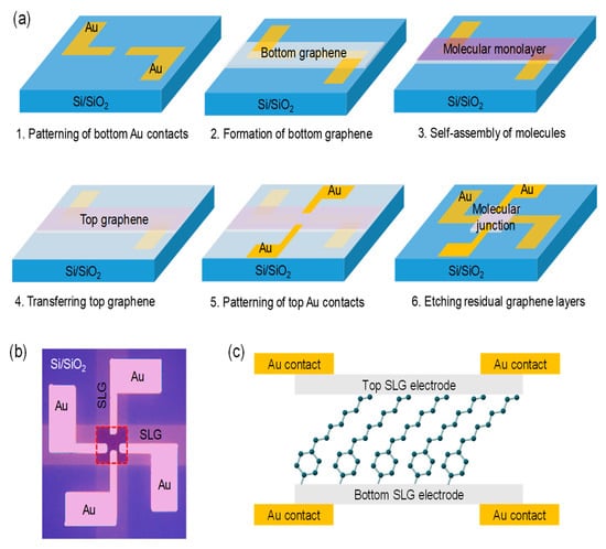
Figure 1.
(a) Illustration of the fabrication process (step 1 to step 6) of the vertically stacked graphene/arylalkane/graphene device. (b) Optical image of a complete device. Red dashed square denotes the area of an active junction, which was estimated to be 250 × 250 μm2. (c) Schematic of the device structure in a cross-sectional view. The component molecule in the junction is C8.
3. Results and Discussion
The arylalkane molecules were self-assembled on the patterned bottom SLGs by a dediazonization process of sp2 hybridization carbon networks, which can form a robust covalent C−C bond between the molecules and graphene basal planes [21,22]. contrary, the top end of the molecular monolayers was contacted with the top SLGs by means of van der Waals interactions. Figure 1c illustrates the schematic of the complete device structure in a cross-sectional view. The arrangement based on vertically stacked graphene heterostructures showed excellent stability for high-yield devices (>80%) and successive electrical measurements. By performing a line profile analysis of the AFM topographical images (Figure S1 in the Supplementary Materials), the heights of a pristine and C10-grafted graphene layer transferred to the SiO2 surface were measured as 0.5 nm and 2.5 nm, respectively. The height difference of ~2 nm reasonably confirmed the monolayer formation on SLGs, as compared to the molecular length estimated from ChemDraw (CambridgeSoft, Cambridge, MA, USA).
Raman spectroscopy has been extensively used as an analytical technique for the non-destructive investigation of SLGs and their derivatives decorated with the organic molecules [26,27]. We measured the Raman spectra of the pristine and arylalkane-grafted graphenes transferred on the substrates, as shown in Figure 2, which were obtained at 10 different spots with a 532 nm laser. The assigned peak position and intensity in each spectrum were determined by Lorentzian function. The spectrum of the pristine graphene sheet entirely concurred with previously reported results [26], where two prominent peaks of G band (1582 cm−1) and 2D band (2675 cm−1) appeared. The omission of D band (1350 cm−1), typically induced by disorder or defects in the graphene basal plane [27], implied that the CVD graphene was of good quality. A large Raman intensity ratio between 2D and G bands (I2D/IG > 2.4) indicated that the transferred graphene film was a single layer [28]. Noticeably, the Raman peak corresponding to D band appeared after the attachment of the arylalkane molecules to SLGs. The D peak can be caused by increased defects resulting from the formation of a covalent C–C sp3 bond between the molecules and SLGs [22]. After molecular deposition, we also observed that the intensity ratio of the 2D band against the G band (I2D/IG) decreased, and the position of the G peak was downshifted (Figure S2 in the Supplementary Materials). It has been reported that such a decrease in the ratio of I2D/IG results from a molecular doping effect and G peak’s shift to lower frequency, namely, softening of the G band indicates electron donating on graphene [29]. Collectively, our observation in the Raman spectra consistently showed the signatures of molecular layer formation on SLGs.
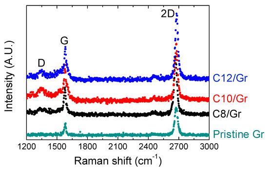
Figure 2.
Raman spectra of pristine and arylalkane (C8, C10 and C12)-grafted graphenes transferred to SiO2 surface.
The alkyl chains with different lengths constitute an important control series in molecular junctions, because a coherent picture has been clearly established for the non-resonant tunneling mechanism and length-dependent transport characteristics with the alkyl-based molecules [2,12,23]. We performed electrical measurements on a total of 294 fabricated devices (78 for C8, 105 for C10, and 111 C for 12), excluding open- or short-circuit failures (38 devices). The current density (J)−voltage (V) data collected by measuring enough devices provided the statistical picture of molecular electronic properties in the vertical junctions. Figure 3a displays the current density histograms of C8, C10 and C12 junctions measured at 2 V, which fitted well with the Gaussian curves. The intact statistics, without any device selection, showed that the J values were log-normally distributed. The peak positions of Gaussian curves in the histograms represented the most probable value of the current density for each junction, manifesting distinct molecular length dependency. We note that the log-normal distribution derives from the primary factor exponentially affecting the current density. It would probably be the variation in the tunneling distance that can be influenced by the detailed microscopic configurations, such as a molecular binding site and conformation in the junctions [2]. Such a result was not monitored in the graphene–graphene structure with the absence of component molecules, but rather its histogram indicated Gaussian distribution at the linear scale (not shown here). Figure 3b displays the statistically representative J−V curve on a log scale, which was generated by averaging the junctions within three sigma (3σ) regimes of the Gaussian distribution in Figure 3a [30]. The error bar indicates standard deviation from the averaged J value. The current density of the molecular junctions appeared to be much lower than that of the direct graphene–graphene (Gr–Gr) contact (top data in Figure 3b). For the shortest C8 junction, it was reduced by a factor of ~103 in A/m2 unit, denoting the formation of a transport barrier sandwiched between two SLGs. In addition, Figure 3b shows that the current density of the molecular junctions rapidly decreased as the number of carbons in the alkyl chains increased, which accorded with the characteristic of tunneling [23].
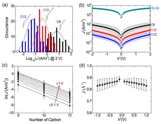
Figure 3.
(a) Statistical histograms of the current density at 2 V for C8, C10 and C12 junctions. The peak position of Gaussian distribution indicates the most probable value for each junction. (b) Statistical representative J−V curves on a log scale, obtained from the devices within 3σ regimes of Gaussian distribution. The error bars denote the standard deviation for averaging. (c) Plots of ln(J) versus the number of carbons at different voltages. β is determined by the slopes of the linear fits. (d) Plots of the β values from −1 V to 1 V. Error bars denote the uncertainty about the linear fits.
To investigate the length-dependent charge transport of the junctions in more detail, we presented the semi-log plot of current density (−1 to +1 V) as a function of the molecular length, as shown in Figure 3c. Within the simplified Simmons model for trapezoidal barrier approximation, the molecular tunneling junction is typically described by J ∝ exp(−βd), where β is the tunneling decay coefficient and d is the molecular length. β mathematically scales with the square root of the barrier height and quantifies the decay of the tunneling probability with increasing d [23], depending on the molecular structure. Furthermore, the decay coefficient is reproducible across various experimental platforms [24], which can accordingly provide a valuable benchmark for the formation of a valid molecular junction. Figure 3c reveals an apparent exponential relationship existing between J and d, corresponding to J ∝ exp(−βd), where the tunneling decay parameter was obtained from the slopes of the linear fits in Figure 3c. As plotted in Figure 3d, the β values were estimated to be 1.04 to 1.12 per carbon (equal to 0.83 to 0.89 Å−1). The error bar denotes uncertainty about the linear fits. These β values were reasonably consistent with those observed in conventional metal/alkyl-containing monolayer/metal junctions [16,23,24]. Despite still being within the range of uncertainty, a subtle reduction in β with increasing voltage may be ascribed to a large electric field-induced barrier lowering in the tunneling junctions [31]. It is also noteworthy that a few recent studies on the rough topographic condition of the bottom electrodes have shown a significantly lower β value (~0.5 Å−1), even for alkyl-based junctions [7,32]. In this context, we checked the surface roughness of a graphene layer transferred on the oxidized Si substrate using AFM (Figure S3 in the Supplementary Materials). The root mean square (r.m.s.) roughness was estimated to be ∼0.14 nm. Such a smooth graphene surface would be desirable to obtain an accurate β value.
The independence of J−V characteristics on temperature variation is a well-known verification of charge tunneling, because it can eliminate many of the other thermally activated transport mechanisms, for example, thermionic emission or hopping conduction [11,23]. The temperature-variable measurement (80 to 280 K) of J−V curves on C8 junctions is shown in Figure 4a. Figure 4b displays corresponding Arrhenius plots and logarithmic J versus inverse temperatures, transformed from the data in Figure 4a. No temperature dependency of the J−V characteristics was clearly confirmed. This result demonstrates that the charge transport occurred by tunneling via the molecular monolayer incorporated into two SLGs. A coherent and clear picture of non-resonant tunneling has, so far, emerged for alkyl-based molecular junctions, because the EF easily lies in the large HOMO−LUMO gap (8~10 eV) of the very short molecule [2,24].
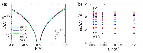
Figure 4.
(a) Representative J−V curves of the C8 junction on a semi-log scale as the temperature varies from 80 to 280 K. (b) Arrhenius plots of the current density at different voltages from 0.1 to 1 V.
Transition voltage spectroscopy (TVS) facilitates an evaluation of the difference (|ε0 − EF|) between the nearest molecular energy level (ε0) and EF [33,34], which refers to the height of a transport barrier in the junctions, by estimating the transition voltage (Vt) to produce an inflection point of the nonlinear Fowler—Nordheim (FN) plot, namely, ln(J/V2) versus 1/V (see the Supplementary Materials for details). Since its first introduction [33], TVS has become a prevailing analytical technique to study the energy level alignment in molecular junctions, due to its simplicity and validity. Interpretation of the FN curves based on the Landauer transport model showed that such inflection can take place when ε0 (HOMO for this case) is quite close to a resonance position by the bias voltage (Figure 5a) [35], where it seems to be in the Lorentzian shape broadened by the coupling with electrodes [30]. Accordingly, a measurement of Vt offers experimental approximation to |ε0− EF|. Figure 5b shows the representative TVS analysis of C8, C10 and C12 junctions. The minimum point on the FN curves refers to Vt (as marked by arrows). A TVS histogram of the inflection events was constructed from these minimum values (Figure 6a–c), in which the Gaussian distribution showed no significant asymmetry for the bias polarity. This effect was observed in the molecular junctions, which have comparable coupling strengths for both molecule–electrode contacts [34], thus indicating that the graphene-based vertical molecular junctions can provide good stability for the top physical contacts via van der Waals interactions [36]. A graphical summary of the TVS measurement on the arylalkane junctions is shown in Figure 6d. It can be clearly observed that the average of Vt (point data with error bar) fell within the standard deviation (dashed lines) of the values measured in each junction. This result demonstrated that Vt was not dependent on the molecular length. Similarly, a study of ultraviolet photoelectron spectroscopy using alkyl thiol monolayers on the Au surface showed that the energy offset (|εHOMO − EF|) of HOMO and EF was independent of the alkyl chain’s length [33]. The constancy of Vt in alkyl-based molecular junctions with variable lengths exactly coincided with the Landauer transport model of TVS, where it was invariant for constant |ε0 − EF| [37], whereas it decreased as the tunneling gap in a molecule-free vacuum junction increased, complying with the Simmons model [38]. Consequently, the findings of the TVS analysis presented further evidence of molecular barrier formation in the vertical tunneling junctions.
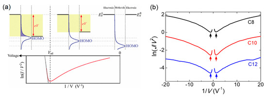
Figure 5.
(a) Illustration of the inflection behavior in the FN curve and corresponding energy band diagrams. The inflection voltage Vinfl (vertically dashed line) in the FN curve denotes the transition voltage. Reproduced from Ref. [29], with permission from American Physical Society. (b) Representative TVS analysis of C8, C10 and C12 junctions. Each arrow indicates the transition voltage.
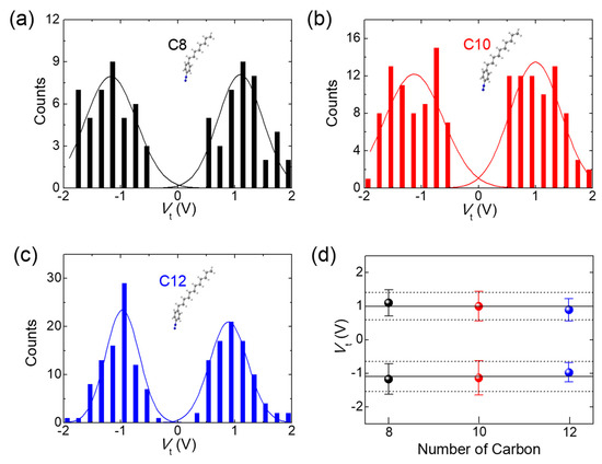
Figure 6.
Statistical TVS histograms of (a) C8, (b) C10 and (c) C12 junctions. The solid curves indicate Gaussian distribution, where no significant asymmetry was observed. (d) Graphical summary of TVS measurement on the arylalkane junctions. The transition voltage of the junctions was independent of the molecular length.
4. Conclusions
In summary, we reported an alternative molecular device architecture using graphene heterostructures. Our prototype devices were the SLG electrode-based molecular junctions with arylalkane molecules acting as a vertical tunneling barrier. They, indeed, exhibited intrinsic molecular charge transport characteristics with a working device yield of more than 80% among all the fabricated devices. Such devices have considerable potential for a versatile test platform in molecular electronics. We showed inherent molecular contribution to the charge tunneling in the junctions by accomplishing various characterization techniques: (1) intact statistical analysis, (2) J−V curves independent of temperature variation, (3) accurate exponential decay of the current density with the length of alkyl chains, and (4) the TVS analysis coincided with the Landauer transport model, which fully demonstrated that arylalkane molecules acted as a controllable transport barrier in the vertical junctions, by which one can constitute a valid molecular electronic device with SLG electrodes. The intrinsic tunneling characteristics indicate that the integrity of the component molecular layer as a tunnel barrier is preserved in the fabricated device, and the charge transport is not dominated by defects and imperfections. As demonstrated by our findings, the graphene contacts effectively protect the molecular layer from penetration of the evaporated metal atoms and preserve its integrity in the junction, offering a reliable test platform for molecular charge transport characterization. In addition, the application of a back-gate electrode to the graphene-based molecular junctions, to actively control the tunneling transport, suggests promising avenues for future studies.
Supplementary Materials
The following supporting information can be downloaded at: https://www.mdpi.com/article/10.3390/cryst12060787/s1, Figure S1: AFM topographical images and line profile analyses; Figure S2: Intensity ratio and shift of Raman peak; Figure S3: Surface roughness; Figure S4: Representative J−V curves of C10 and C12 junctions.
Author Contributions
Conceptualization, H.S.; Investigation, S.-H.H. and D.-H.S.; Methodology, S.-H.H. and D.-H.S.; Supervision, H.S.; Writing–original draft, H.S.; Writing–review & editing, S.-H.H., D.-H.S. and H.S. All authors have read and agreed to the published version of the manuscript.
Funding
This work was supported by National Research Foundation of Korea (grant No. 2020R1F1A1076107).
Institutional Review Board Statement
Not applicable.
Informed Consent Statement
Not applicable.
Data Availability Statement
Data is contained within the article or supplementary material.
Conflicts of Interest
The authors declare no conflict of interest.
References
- Evers, F.; Korytár, R.; Tewari, S.; van Ruitenbeek, J.M. Advances and challenges in single-molecule electron transport. Rev. Mod. Phys. 2020, 92, 035001. [Google Scholar] [CrossRef]
- Vilan, A.; Aswal, D.; Cahen, D. Large-Area, Ensemble Molecular Electronics: Motivation and Challenges. Chem. Rev. 2017, 117, 4248–4286. [Google Scholar] [CrossRef] [PubMed]
- Han, Y.; Nickle, C.; Zhang, Z.; Astier, H.P.A.G.; Duffin, T.J.; Qi, D.; Wang, Z.; del Barco, E.; Thompson, D.; Nijhuis, C.A. Electric-field-driven dual-functional molecular switches in tunnel junctions. Nat. Mater. 2020, 19, 843–848. [Google Scholar] [CrossRef] [PubMed]
- Song, P.; Guerin, S.; Tan, S.J.R.; Annadata, H.V.; Yu, X.J.; Scully, M.; Han, Y.M.; Roemer, M.; Loh, K.P.; Thompson, D.; et al. Stable Molecular Diodes Based on π–π Interactions of the Molecular Frontier Orbitals with Graphene Electrodes. Adv. Mater. 2018, 30, 1706322. [Google Scholar] [CrossRef] [PubMed]
- Song, H. Electrostatic Gate Control in Molecular Transistors. Top. Curr. Chem. 2018, 376, 37. [Google Scholar] [CrossRef] [PubMed]
- Qiu, X.; Chiechi, R.C. Large-Area Molecular Junctions: Synthesizing Integrated Circuits for Next-Generation Nonvolatile Memory. Trends Chem. 2020, 2, 869–872. [Google Scholar] [CrossRef]
- Seo, S.; Min, M.; Lee, S.M.; Lee, H. Photo-switchable molecular monolayer anchored between highly transparent and flexible graphene electrodes. Nat. Commun. 2013, 4, 1920. [Google Scholar] [CrossRef] [Green Version]
- Park, S.; Kim, H.R.; Kim, J.; Hong, B.-H.; Yoon, H.J. Enhanced Thermopower of Saturated Molecules by Noncovalent Anchor-Induced Electron Doping of Single-Layer Graphene Electrode. Adv. Mater. 2021, 33, 2103177. [Google Scholar] [CrossRef]
- Wan, A.; Jiang, L.; Sangeeth, C.S.S.; Nijhuis, C.A. Reversible Soft Top-Contacts to Yield Molecular Junctions with Precise and Reproducible Electrical Characteristics. Adv. Funct. Mat. 2014, 24, 4442–4456. [Google Scholar] [CrossRef]
- Jie, Y.; Wang, D.; Huang, J.; Feng, Y.; Yang, J.; Fang, J.; Chen, R. Metal–Molecule–Metal Junctions on Self-Assembled Monolayers Made with Selective Electroless Deposition. ACS Appl. Mater. Inter. 2022, 14, 1609–1614. [Google Scholar] [CrossRef]
- Jeong, H.; Kim, D.; Xiang, D.; Lee, T. High-Yield Functional Molecular Electronic Devices. ACS Nano 2017, 11, 6511–6548. [Google Scholar] [CrossRef] [PubMed]
- Song, H.; Lee, T.; Choi, N.-J.; Lee, H. A statistical method for determining intrinsic electronic transport properties of self-assembled alkanethiol monolayer devices. Appl. Phys. Lett. 2007, 91, 253116. [Google Scholar] [CrossRef]
- Wang, G.; Kim, Y.; Choe, M.; Kim, T.-W.; Lee, T. A New Approach for Molecular Electronic Junctions with a Multilayer Graphene Electrode. Adv. Mater. 2011, 23, 755–760. [Google Scholar] [CrossRef]
- Koo, J.; Jang, Y.; Martin, L.; Kim, D.; Jeong, H.; Kang, K.; Lee, W.; Kim, J.; Hwang, W.-T.; Xiang, D.; et al. Unidirectional Real-Time Photoswitching of Diarylethene Molecular Monolayer Junctions with Multilayer Graphene Electrodes. ACS Appl. Mater. Inter. 2019, 11, 11645–11653. [Google Scholar] [CrossRef] [PubMed]
- Min, M.; Seo, S.; Lee, S.M.; Lee, H. Voltage-Controlled Nonvolatile Molecular Memory of an Azobenzene Monolayer through Solution-Processed Reduced Graphene Oxide Contacts. Adv. Mater. 2013, 25, 7045. [Google Scholar] [CrossRef]
- Akkerman, H.B.; Blom, P.W.M.; de Leeuw, D.M.; de Boer, B. Towards molecular electronics with large-area molecular junctions. Nature 2006, 441, 69–72. [Google Scholar] [CrossRef] [PubMed] [Green Version]
- Jeong, H.; Kim, D.; Kim, P.; Cho, M.R.; Hwang, W.-T.; Jang, Y.; Cho, K.; Min, M.; Xiang, D.; Park, Y.D.; et al. A new approach for high-yield metal–molecule–metal junctions by direct metal transfer method. Nanotechnology 2015, 26, 025601. [Google Scholar] [CrossRef]
- Jang, Y.; Kwon, S.-J.; Shin, J.; Jeong, H.; Hwang, W.-T.; Kim, J.; Koo, J.; Ko, T.Y.; Ryu, S.; Wang, G.; et al. Interface-Engineered Charge-Transport Properties in Benzenedithiol Molecular Electronic Junctions via Chemically p-Doped Graphene Electrodes. ACS Appl. Mater. Inter. 2017, 9, 42043–42049. [Google Scholar] [CrossRef]
- Chen, S.; Su, D.; Jia, C.; Li, Y.; Li, X.; Guo, X.; Leigh, D.A.; Zhang, L. Real-time observation of the dynamics of an individual rotaxane molecular shuttle using a single-molecule junction. Chem 2022, 8, 243–252. [Google Scholar] [CrossRef]
- Novoselov, K.S.; Fal′ko, V.I.; Colombo, L.; Gellert, P.R.; Schwab, M.G.; Kim, K. A roadmap for graphene. Nature 2012, 490, 192–200. [Google Scholar] [CrossRef]
- Liu, Y.C.; McCreery, R.L. Reactions of Organic Monolayers on Carbon Surfaces Observed with Unenhanced Raman Spectroscopy. J. Am. Chem. Soc. 1995, 117, 11254–11259. [Google Scholar] [CrossRef]
- MacLeod, J.M.; Rosei, F. Molecular Self-Assembly on Graphene. Small 2014, 10, 1038–1049. [Google Scholar] [CrossRef] [PubMed]
- Wang, W.; Lee, T.; Reed, M.A. Mechanism of electron conduction in self-assembled alkanethiol monolayer devices. Phys. Rev. B 2003, 68, 035416. [Google Scholar] [CrossRef]
- Xie, Z.; Bâldea, I.; Frisbie, C.D. Energy Level Alignment in Molecular Tunnel Junctions by Transport and Spectroscopy: Self-Consistency for the Case of Alkyl Thiols and Dithiols on Ag, Au, and Pt Electrodes. J. Am. Chem. Soc. 2019, 141, 18182–18192. [Google Scholar] [CrossRef] [PubMed]
- Liang, X.; Sperling, B.A.; Calizo, I.; Cheng, G.; Hacker, C.A.; Zhang, Q.; Obeng, Y.; Yan, K.; Peng, H.; Li, Q.; et al. Toward Clean and Crackless Transfer of Graphene. ACS Nano 2011, 5, 9144–9153. [Google Scholar] [CrossRef] [PubMed]
- Malard, L.M.; Pimenta, M.A.; Dresselhaus, G.; Dresselhaus, M.S. Raman spectroscopy in graphene. Phys. Rep. 2009, 473, 51–87. [Google Scholar] [CrossRef]
- Wu, J.-B.; Lin, M.-L.; Cong, X.; Liu, H.-N.; Tan, P.-H. Raman spectroscopy of graphene-based materials and its applications in related devices. Chem. Soc. Rev. 2018, 47, 1822–1873. [Google Scholar] [CrossRef] [Green Version]
- Graf, D.; Molitor, F.; Ensslin, K.; Stampfer, C.; Jungen, A.; Hierold, C.; Wirtz, L. Spatially Resolved Raman Spectroscopy of Single- and Few-Layer Graphene. Nano Lett. 2007, 7, 238. [Google Scholar] [CrossRef] [Green Version]
- Dong, X.; Fu, D.; Fang, W.; Shi, Y.; Chen, P.; Li, L.-J. Doping Single-Layer Graphene with Aromatic Molecules. Small 2009, 5, 1422–1426. [Google Scholar] [CrossRef]
- Reus, W.F.; Nijhuis, C.A.; Barber, J.R.; Thuo, M.M.; Tricard, S.; Whitesides, G.W. Statistical Tools for Analyzing Measurements of Charge Transport. J. Phys. Chem. C 2012, 116, 6714–6733. [Google Scholar] [CrossRef] [Green Version]
- Tung, R.T. The physics and chemistry of the Schottky barrier height. Appl. Phys. Rev. 2014, 1, 011304. [Google Scholar]
- Yuan, L.; Jiang, L.; Zhang, B.; Nijhuis, C.A. Dependency of the Tunneling Decay Coefficient in Molecular Tunneling Junctions on the Topography of the Bottom Electrodes. Angew. Chem. Int. Ed. 2014, 53, 3377–3381. [Google Scholar] [CrossRef] [PubMed]
- Beebe, J.M.; Kim, B.; Gadzuk, J.W.; Frisbie, C.D.; Kushmerick, J.G. Transition from Direct Tunneling to Field Emission in Metal-Molecule-Metal Junctions. Phys. Rev. Lett. 2006, 97, 026801. [Google Scholar] [CrossRef] [Green Version]
- Bâldea, I. Ambipolar transition voltage spectroscopy: Analytical results and experimental agreement. Phys. Rev. B 2012, 85, 035442. [Google Scholar] [CrossRef] [Green Version]
- Araidai, M.; Tsukada, M. Theoretical calculations of electron transport in molecular junctions: Inflection behavior in Fowler-Nordheim plot and its origin. Phys. Rev. B 2010, 81, 235114. [Google Scholar] [CrossRef]
- Song, P.; Sangeeth, C.S.S.; Thompson, D.; Du, W.; Loh, K.P.; Nijhuis, C.A. Noncovalent Self-Assembled Monolayers on Graphene as a Highly Stable Platform for Molecular Tunnel Junctions. Adv. Mater. 2016, 28, 631–639. [Google Scholar] [CrossRef] [PubMed]
- Huisman, E.H.; Guédon, C.M.; van Wees, B.J.; van der Molen, S.J. Interpretation of Transition Voltage Spectroscopy. Nano Lett. 2009, 9, 3909–3913. [Google Scholar] [CrossRef] [Green Version]
- Trouwborst, M.L.; Martin, C.A.; Smit, R.H.M.; Guédon, C.M.; Baart, T.V.; van der Molen, S.J.; van Ruitenbeek, J.M. Transition Voltage Spectroscopy and the Nature of Vacuum Tunneling. Nano Lett. 2011, 11, 614–617. [Google Scholar] [CrossRef] [Green Version]
Publisher’s Note: MDPI stays neutral with regard to jurisdictional claims in published maps and institutional affiliations. |
© 2022 by the authors. Licensee MDPI, Basel, Switzerland. This article is an open access article distributed under the terms and conditions of the Creative Commons Attribution (CC BY) license (https://creativecommons.org/licenses/by/4.0/).