Abstract
We investigated the types of dendrites grown in Si1−xGex (0 < x < 1) melts, and also investigated the initiation of dendrite growth during unidirectional growth of Si1-xGex alloys. Si1−xGex (0 < x < 1) is a semiconductor alloy with a completely miscible-type binary phase diagram. Therefore, Si1−xGex alloys are promising for use as epitaxial substrates for electronic devices owing to the fact that their band gap and lattice constant can be tuned by selecting the proper composition, and also for thermoelectric applications at elevated temperatures. On the other hand, regarding the fundamentals of solidification, some phenomena during the solidification process have not been clarified completely. Dendrite growth is a well-known phenomenon, which appears during the solidification processes of various materials. However, the details of dendrite growth in Si1−xGex (0 < x < 1) melts have not yet been reported. We attempted to observe dendritic growth in Si1−xGex (0 < x < 1) melts over a wide range of composition by an in situ observation technique. It was found that twin-related dendrites appear in Si1−xGex (0 < x < 1) melts. It was also found that faceted dendrites can be grown in directional solidification before instability of the crystal/melt interface occurs, when a growing crystal contains parallel twin boundaries.
1. Introduction
Dendrite crystals appear in the solidification processes of various materials including metals [1,2,3], metallic alloys [4,5,6,7,8,9,10], semiconductors [11,12,13,14,15,16,17,18,19], organic materials [20,21,22,23,24,25], and so on. It has been shown that the growth shapes and growth mechanisms of dendrites are different between metallic alloys [26,27] and semiconductors [13,18]. Although the solute and thermal diffusion in the liquid are key in determining the growth shape and growth velocity of dendrites in metallic alloys, the kinetics of atomic attachment at the reentrant corner formed at the front of dendrites due to the existence of twin boundaries determines the growth shape and growth velocity of dendrites in semiconductors. The typical shape of alloy dendrites is schematically shown in Figure 1a. Generally, a dendrite grows in a preferential direction to form a primary arm, and secondary arms extend from the side of the primary arm. On the other hand, the growth shape of the dendrites of semiconductor materials, such as Si and Ge, are different from that of metal alloy dendrites, as shown schematically in Figure 1b. At least two parallel twin boundaries exist at the center of the dendrites, the surface of the dendrites is bounded by facet planes, and the preferential growth direction is <112> or <110>, which is related to the existence of parallel twin boundaries [13,18]. This type of dendrite is called a “faceted dendrite” or “twin-related faceted dendrite”. Nagashio et al. showed that Si dendrites can grow preferentially in the <100> direction (<100> dendrite) in a highly undercooled melt when the extent of undercooling (ΔT) is more than 100 K [17]. The growth shape of <100> dendrites of Si is similar to that of alloy dendrites, that is, the <100> dendrite does not contain any twin boundaries (twin-free dendrite). To realize such a highly undercooled melt, a container-less levitation method was used [17]. In a normal solidification process using a container (crucible), it is difficult to maintain the melt in a highly undercooled state. Therefore, only faceted dendrites appear in the lower undercooling region, such as ΔT ≃ 10 K [28], in the solidification process of pure Si in a crucible. Recently, we directly observed the growth shape of dendrites of GaSb, which is a compound semiconductor with the zinc blende structure [19]. The growth scheme of GaSb dendrites could be explained by the Si faceted dendrite model. Thus, it has been shown that the types of dendrites depend on the material.
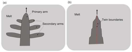
Figure 1.
Growth shape of dendrites of (a) metallic alloys and (b) semiconductors.
Si1−xGex (0 < x < 1) is a semiconductor alloy with a completely miscible-type binary phase diagram. Si1−xGex alloys are promising for use as epitaxial substrates of electronic devices owing to the fact that their band gap and lattice constant can be tuned by selecting the proper composition [29,30,31,32,33,34,35], and thus, bulk Si1-xGex single crystals have been obtained from the melt by several methods [36,37,38,39,40,41,42,43,44,45,46,47,48,49,50,51,52,53]. Si-rich Si1-xGex alloys (0.2 ≲ x ≲ 0.3) are promising for thermoelectric applications at elevated temperatures [54,55,56,57,58,59,60], and have also been considered for use in solar cells [61,62]. On the other hand, knowledge of the fundamentals of solidification for Si1−xGex alloys, including dendrite growth, is still limited. Miller et al. investigated cellular growth of Ge-rich Si1−xGex single crystals by a phase-field simulation [63]. We reported on the instability of the crystal/melt interface during directional solidification [64,65,66] and re-melting phenomena during rapid solidification processes [67] in Si-rich Si1−xGex. Herlach et al. reported on the crystallization process from highly undercooled Si-Ge melts using a container-less levitation method [68]. They focused on the transition of the growth mode as a function of undercooling and reported that the critical undercooling, where the interface shape changed from faceted to dendritic and dendritic to planar, occurred in a highly undercooled region (45K < ΔT < 315K). However, details on the dendrite growth of Si1−xGex (0 < x < 1) alloys over a wide range of composition have not yet been reported. In particular, we are interested in the type of dendrites that are formed in Si1−xGex (0 < x < 1) alloys. Si1−xGex can form a solid solution over a wide range, and thus there is the possibility to grow metallic alloy-type dendrites (twin-free dendrites), which were observed in pure Si in highly undercooled melts [17]. On the other hand, Si1−xGex is also a faceted material like pure Si, pure Ge, and GaSb, and thus faceted dendrites (twin-related dendrites) could be grown.
Based on this fundamental interest, in this study we attempted to observe dendritic growth in Si1−xGex (0 < x < 1) melts over a wide range of composition using an in-situ observation technique. Also, it is crucial to maintain a planar crystal/melt interface during a directional solidification for the growth of bulk Si1−xGex ingots. Therefore, we performed directional solidification experiments to investigate when dendrite growth appears at the crystal/melt interface during directional solidification.
2. Experimental Procedures
An in situ observation system composed of a furnace and a digital optical microscope was used for the experiments [69]. Pure Si (99.9999%) and Ge (99.999%) were mixed with different compositions. Before the experiments, both of the raw materials were cleaned. First, they were ultrasonically cleaned in acetone to remove oil components from the surface. After rinsing with ultrapure water, the samples were dipped into aqueous HF solution to remove the surface oxide layer. Then, the cleaned Si and Ge were put into a silica crucible with a size of 22 × 12 × 11 mm, which was placed into a furnace. The furnace has a window to observe the sample surface by means of the digital optical microscope. The furnace temperature was controlled by two zone graphite heaters. After melting of the raw materials, the temperature was kept for 30 min at higher than the melting temperature to allow the mixing of Si and Ge. Then, the inside of the furnace was cooled to promote solidification.
We performed two experiments as follows. First, we simply cooled the whole melt at 20 °C/min just to observe the growth shape of the dendrites over a wide composition range to investigate the types of dendrites formed. Next, we carried out directional solidification experiments to investigate when dendrite growth appears at the crystal/melt interface during directional solidification. After the melting and mixing processes of the raw materials, we adjusted the temperature difference between the two zone heaters to 20 °C. Then, the temperature was gradually decreased while maintaining the temperature difference, and crystallization was started from one side of the crucible.
The solidification processes in each sample were monitored and recorded by PC. After the solidification, orientation analysis was performed by the SEM-EBSP (Scanning Electron Microscopy-Electron Back Scattering diffraction Pattern) method.
3. Results and Discussion
We directly observed the growth shape of dendrites in Si1−xGex (0 < x < 1) melts cooled at 20 °C/min. Figure 2a shows a dendrite grown from a Si0.7Ge0.3 melt. For comparison, a dendrite grown from a pure Si melt is also shown in Figure 2b. The growth shapes of the dendrites are similar; the surfaces of the dendrites are surrounded by well-developed facets, and there are no branches on the side of the dendrites like those seen for alloy dendrites (Figure 1a). It was also observed that twin boundaries existed at the center part of the dendrite, as indicated by the arrow in the middle picture in Figure 2a. To confirm this, orientation analysis was performed using the SEM-EBSP method after solidification. Figure 3 shows an SEM image of the dendrite (left figure) and the results of SEM-EBSP analysis performed at the center of this dendrite (right figures). The analyzed area is indicated by a dotted red square in the SEM image. The colored figure shows an orientation map and the gray image below the orientation map shows the grain boundary types as colored lines. It was found that two Σ3 twin boundaries, indicated by red lines, existed in the dendrite. Therefore, it was confirmed that the dendrite observed in Figure 2a was similar to Si faceted dendrites. Similar experiments were conducted over a wide range of composition for Si1−xGex (0 < x < 1) melts. Figure 4 shows dendrites grown from Si1−xGex (0 < x < 1) melts with different compositions. Dendrites could be observed in all samples. In all cases, the growth shapes of dendrites were similar to those of Si faceted dendrites, and not similar to the shape of alloy dendrites. We also confirmed the existence of parallel twin boundaries in the dendrites by SEM-EBSP analysis after the solidification as in Figure 3. Nagashio et al. observed alloy-type dendrites in the solidification of pure Si in a highly undercooled melt at ΔT > 100K. They realized such a highly undercooled melt using a container-less levitation method [17]. Unfortunately, our experimental system is not equipped with a measurement system able to measure the melt temperature directly. Therefore, the degree of undercooling at the initiation of dendrite growth could not be determined. However, one can understand that because we used a crucible, it was difficult to maintain a melt in a highly undercooled state.
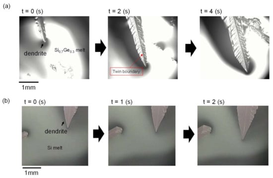
Figure 2.
In situ observations of growing dendrites in (a) Si0.7Ge0.3 melt and (b) pure Si melt.
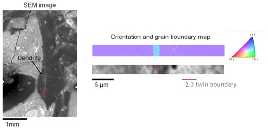
Figure 3.
Structural analysis of dendrite observed in Si0.7Ge0.3 melt by SEM-EBSP. The SEM image is shown at the left. The orientation map is shown at the upper right, and the grain boundary characteristics in the region of the dotted red box in the SEM image at the lower right.
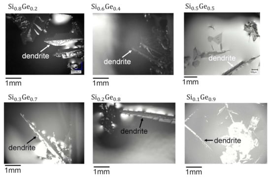
Figure 4.
Growth shape of dendrites in Si1−xGex (0 < x < 1) melts with various compositions.
As above, it was shown that the dendrites grown in the Si1−xGex (0 < x < 1) melts in a solidification process (in a crucible) were twin-related faceted dendrites, similar to those in pure Si and Ge. In order to grow a faceted dendrite, a crystal must contain twin boundaries. It is known that the stacking fault energies of Si (around 30~50 mJm−2 [70,71]) and Ge (around 50~60 mJm−2 [70,71]) are quite low, and that of Si1−xGex (0 < x < 1) is between these values [71]. Therefore, it appears that twin boundaries are easily generated in the crystal during the solidification, which leads to the appearance of faceted dendrite growth.
Next, we performed directional growth experiments to observe the crystal/melt interface of Si1−xGex alloys for the investigation of the effect of twin boundaries on the shape of the crystal/melt interface. According to the theory of Mullins–Sekerka interface instability [72], the interface shape is determined by the temperature gradient in the melt at the interface, as schematically explained in Figure 5. Figure 5a shows the case where the planar interface is maintained in a positive temperature gradient in the melt at the interface. In this case, when a fluctuation is generated at the planar interface, as in the middle figure of Figure 5a, the growth velocity at the tip of the fluctuation is lower than that at the bottom part due to the lower degree of undercooling, and thus, the bottom part will catch up with the tip and a planar interface is maintained. On the other hand, Figure 5b shows the case where a zigzag faceted interface is formed under a negative temperature gradient. In this case, the growth velocity at the tip of the fluctuation at the interface becomes higher than that at the bottom part, as shown in the middle of Figure 5b, and thus the fluctuation is amplified to form a zigzag faceted interface. In case of non-faceted materials, the interface shape transforms from planar to cellular (or dendritic) under the negative temperature gradient, as also schematically shown in Figure 5b. This transformation of the interface shape from planar to wavy to cellular or zigzag faceted is well known as Mullins–Sekerka instability (instability of the crystal/melt interface) [72]. It was experimentally confirmed in pure Si single crystals [73].
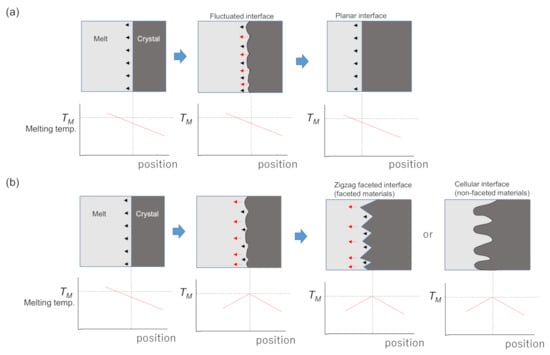
Figure 5.
Schematic illustration of the shape transformation of crystal/melt interfaces. (a) A planar interface is maintained due to a positive temperature gradient in the melt at the interface, and (b) a zigzag faceted or cellular interface is formed due to a negative temperature gradient.
It was also reported that the instability of a crystal/melt interface like Figure 5b is initiated at a portion of the grain boundary in multi-crystalline Si due to the difference in thermal conductivity between the interior of the crystal grain and the grain boundary [74]. We also observed interface instability for Si-rich Si1−xGex (0 < x < 0.1) alloys [64,65,66]. In that case, it was shown that the critical growth velocity for interface instability to occur becomes lower with increasing Ge composition due to constitutional undercooling, and the transformation of the interface shape followed, as shown in Figure 5b. A question remained: if the growing crystal contains parallel twin boundaries and dendrite growth appears during directional solidification, does the dendrite growth appear before the interface instability or after the instability? Since it is difficult to artificially create parallel twin boundaries, we relied on chance and conducted the experiment many times, and were able to observe an interface with parallel twin boundaries. Figure 6a,b show snapshots of directional solidification from Si1−xGex melts. The two melt compositions are almost the same; (a) Si0.92Ge0.08 and (b) Si0.9Ge0.1. As shown in Figure 6a, the planar interface changed to a zigzag faceted interface due to the interface instability. Similar results for the transformation of the interface shape have been reported in pure Si [73] and Si-rich Si1−xGex [65,66]. In those cases, the growing crystal did not contain parallel twin boundaries. On the other hand, when the growing crystal contained parallel twin boundaries (Figure 6b), dendrite growth appeared at a portion of the parallel twin boundaries, while a planar interface was maintained for the other part. This shows that the dendrite growth appears before interface instability occurs. According to the Mullins–Sekerka theory, as explained in Figure 5, interface instability appears under a negative temperature gradient in the melt at the crystal/melt interface, while a planar interface is maintained under a positive temperature gradient [63], which was experimentally confirmed in single crystal Si [73]. The result observed in Figure 6b shows that the planar interface is maintained in the portion without dendrite growth; thus, the temperature gradient appeared to be positive. This result agrees with our previous report for pure Si crystals containing twin boundaries [75].
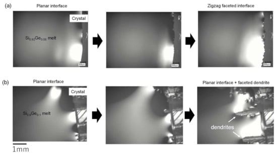
Figure 6.
Observation of interface shape transformation in Si1−xGex alloys. (a) The planar interface changed to a zigzag faceted interface due to the instability. (b) Faceted dendrites appear from the planar interface due to the existence of parallel twin boundaries.
Therefore, it was indicated that dendrite growth appears even in a positive temperature gradient when a crystal contains parallel twin boundaries, as shown in Figure 7. In this case, the amount of undercooling at the tip of the dendrite is smaller than that at the planar interface; however, the atomic attachment at the tip of the dendrite is known to be much faster than that at the planar interface due to the formation of a reentrant corner at the dendrite tip [18], and thus a dendrite can be grown.
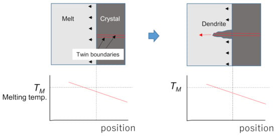
Figure 7.
Formation of the dendritic interface due to the existence of parallel twin boundaries.
5. Conclusions
We investigated dendrite growth in Si1−xGex (0 < x < 1) alloys by in situ observation. Twin-related faceted dendrites appear in melt growth of Si1−xGex (0 < x < 1), which is similar to the case with pure Si and pure Ge. Dendrite growth appears to occur from a planar crystal/melt interface during directional solidification when a Si1−xGex crystal contains a parallel twin boundary. This indicates that a planar interface is not maintained even under a positive temperature gradient when the growing crystal contains parallel twin boundaries.
Author Contributions
Conceptualization, K.F. and M.A.; methodology, K.F. and L.-C.C.; validation, K.F., L.-C.C., K.M., K.S. and H.M.; investigation, G.T. and M.A.; data curation, G.T.; writing—original draft preparation, G.T.; writing—review and editing, K.F., L.-C.C., K.M., K.S. and H.M. All authors have read and agreed to the published version of the manuscript.
Funding
This work was supported by a KAKENHI Grant-in-Aid for Scientific Research (A) (No. 21H04658).
Institutional Review Board Statement
Not applicable.
Informed Consent Statement
Not applicable.
Acknowledgments
We also wish to express our thanks to GIMR collaborative projects in Tohoku University and Joint Research Projects and Seminars under the Bilateral Programs (JSPS(Japan)-DST (India)).
Conflicts of Interest
The authors declare no conflict of interest.
References
- Suzuki, T.; Toyoda, S.; Umeda, T.; Kimura, Y. Dendrite Growth from the Supercooled Melt. J. Cryst. Growth 1977, 38, 123–128. [Google Scholar] [CrossRef]
- Powell, G.L.F.; Colligan, G.A.; Surprenant, V.A.; Urquhart, A. The Growth Rate of Dendrites in Undercooled tin. Metall. Trans. A 1977, A8, 971–973. [Google Scholar] [CrossRef]
- Eckler, K.; Kratz, M.; Egry, I. New Technique of Measuring Dendrite Growth Velocities in Undercooled Metallic Melts. Rev. Sci. Instrum. 1993, 64, 2639–2642. [Google Scholar] [CrossRef]
- McCartney, D.G.; Hunt, J.D. Measurements of Cell and Primary Dendrite Arm Spacings in Directionally Solidified Aluminium Alloys. Acta Metall. 1981, 29, 1851–1863. [Google Scholar] [CrossRef]
- Young, K.P.; Kirkwood, D.H. The Dendrite Arm Spacings of Aluminum-Copper Alloys Solidified under Steady-State Conditions. Metall. Trans. A. 1975, 6, 197–205. [Google Scholar] [CrossRef]
- Jacobi, H.; Schwerdtfeger, K. Dendrite Morphology of Strady State Unidirectionally Solidified Steel. Metall. Trans. A. 1976, 7, 811–820. [Google Scholar] [CrossRef]
- Klaren, C.M.; Verhoeven, J.D.; Trivedi, R. Primary Dendrite Spacing of Lead Dendrites in Pb-Sn and Pb-Au Alloys. Metall. Trans. A. 1980, 11, 1853–1861. [Google Scholar] [CrossRef]
- Mason, J.T.; Verhoeven, J.D.; Trivedi, R. Primary Dendrite Spacing. J. Cryst. Growth 1982, 59, 516–524. [Google Scholar] [CrossRef]
- Gandin, C.-A.; Rappaz, M. A Coupled Finite Element-Cellular Automaton Model for the Prediction of Dendritic Grain Structures in Solidification Processes. Acta Metall. Mater. 1994, 42, 2233–2246. [Google Scholar] [CrossRef]
- Yasuda, H.; Morishita, K.; Nakatsuka, N.; Nishimura, T.; Yoshiya, M.; Sugiyama, A.; Uesugi, K.; Takeuchi, A. Dendrite Fragmentation Induced by Massive-Like Δ-Γ Transformation in Fe-C Alloys. Nat. Commun. 2019, 10, 3183. [Google Scholar] [CrossRef] [Green Version]
- Billig, E. Growth of Monocrystals of Germanium from an Undercooled Melt. Proc. R. Soc. 1955, A229, 346–363. [Google Scholar]
- Bennett, A.I.; Longini, R.L. Dendritic Growth of Germanium Crystals. Phys. Rev. 1959, 116, 53–61. [Google Scholar] [CrossRef]
- Hamilton, D.R.; Seidensticker, R.G. Propagation Mechanism of Germanium Dendrites. J. Appl. Phys. 1960, 31, 1165–1168. [Google Scholar] [CrossRef]
- Wagner, R.S. On the Growth of Germanium Dendrites. Acta Metall. 1960, 8, 57–60. [Google Scholar] [CrossRef]
- Lau, C.F.; Kui, H.W. Microstructures of Undercooled Germanium. Acta Metall. Mater. 1991, 39, 323–327. [Google Scholar] [CrossRef]
- Li, D.; Herlach, D.M. Direct Measurements of Free Crystal Growth in Deeply Undercooled Melts of Semiconducting Materials. Phys. Rev. Lett. 1996, 77, 1801–1804. [Google Scholar] [CrossRef]
- Nagashio, K.; Kuribayashi, K. Growth Mechanism of Twin-Related and Twin-Free Facet Si Dendrites. Acta Mater. 2005, 53, 3021–3029. [Google Scholar] [CrossRef]
- Fujiwara, K.; Maeda, K.; Usami, N.; Nakajima, K. Growth Mechanism of Si-Faceted Dendrites. Phys. Rev. Lett. 2008, 101, 055503. [Google Scholar] [CrossRef]
- Shiga, K.; Kawano, M.; Maeda, K.; Morito, H.; Fujiwara, K. The in situ Observation of Faceted Dendrite Growth During the Directional Solidification of GaSb. Scr. Mater. 2019, 168, 56–60. [Google Scholar] [CrossRef]
- Glicksman, M.E.; Schaefer, R.J.; Ayers, J.D. Dendrite Growth-A Test of Theory. Metall. Trans. A. 1976, 7, 1747–1759. [Google Scholar] [CrossRef]
- Huang, S.-C.; Glicksman, M.E. Fundamentals of Dendritic Solidification-Ⅰ. Steady-State Tip Growth. Acta Metall. 1981, 29, 701–715. [Google Scholar] [CrossRef]
- Esaka, H.; Kurz, W. Columnar Dendrite Growth: Experiments on Tip Growth. J. Cryst. Growth 1985, 72, 578–584. [Google Scholar] [CrossRef]
- Qian, X.W.; Cummins, H.Z. Dendritic Sidebranching Initiation by a Localized Heat Pulse. Phys. Rev. Lett. 1990, 64, 3038–3041. [Google Scholar] [CrossRef]
- Georgelin, M.; Pocheau, A. Onset of Sidebranching in Directional Solidification. Phys. Rev. E. 1998, 57, 3189–3203. [Google Scholar] [CrossRef]
- Akamatsu, S.; Bottin-Rousseau, S.; Perrut, M.; Faivre, G.; Witusiewicz, V.T.; Sturz, L. Real-Time Study of Thin and Bulk Eutectic Growth in Succinonitrile-(D)Camphor Alloys. J. Cryst. Growth 2007, 299, 418–428. [Google Scholar] [CrossRef]
- Trivedi, R.; Kurz, W. Dendritic Growth. Int. Mater. Rev. 1994, 39, 49–74. [Google Scholar] [CrossRef]
- Jaafar, M.A.; Rousse, D.R.; Gibout, S.; Bédécarrats, J.-P. A Review of Dendritic Growth During Solidification: Mathematical Modeling and Numerical Simulations. Renew. Sustain. Energy Rev. 2017, 74, 1064–1079. [Google Scholar] [CrossRef]
- Fujiwara, K.; Maeda, K.; Usami, N.; Sazaki, G.; Nose, Y.; Nomura, A.; Shishido, T.; Nakajima, K. In situ Observation of Si Faceted Dendrite Growth from Low-Degree-of-Undercooling Melts. Acta Mater. 2008, 56, 2663–2668. [Google Scholar] [CrossRef]
- Schäffler, F. High-Mobility Si and Ge Structures. Semicond. Sci. Technol. 1997, 12, 1515–1549. [Google Scholar] [CrossRef]
- Takagi, S. Silicon-Germanium (SiGe)-Based Field Effect Transistors (FET) and Complementary Metal Oxide Semiconductor (CMOS) Technologies. In Silicon-Germanium (SiGe) Nanostructures; Shiraki, Y., Usami, N., Eds.; Woodhead Publishing: Cambridge, UK, 2011; pp. 499–527. [Google Scholar]
- Fitzgerald, E.A.; Xie, Y.-H.; Green, M.L.; Brasen, D.; Kortan, A.R.; Michel, J.; Mii, Y.-J.; Weir, B.E. Totally Relaxed GexSi1-X Layers with Low Threading Dislocation Densities Grown on Si Substrates. Appl. Phys. Lett. 1991, 59, 811–813. [Google Scholar] [CrossRef]
- Vogelsang, T.; Hofmann, K.R. Electron Transport in Strained Si Layers on Si1-XGex Substrates. Appl. Phys. Lett. 1993, 63, 186–188. [Google Scholar] [CrossRef]
- Welser, J.; Hoyt, J.L.; Takagi, S.; Gibbons, J.F. Strain Dependence of the Performance Enhancement in Strained-Si n-Mosfets. Proceedings of 1994 IEEE International Electron Devices Meeting, San Francisco, CA, USA, 11–14 December 1994; pp. 373–376. [Google Scholar]
- Usami, N.; Pan, W.; Fujiwara, K.; Tayanagi, M.; Ohdaira, K.; Nakajima, K. Effect of the Compositional Distribution on the Photovoltaic Power Conversion of Sige Solar Cells. Sol. Energy Mater. Sol. Cells 2007, 91, 123–128. [Google Scholar] [CrossRef]
- Miller, W.; Abrosimov, N.; Rasin, I.; Borissova, D. Cellular Growth of Ge1-X Six Single Crystals. J. Cryst. Growth 2008, 310, 1405–1409. [Google Scholar] [CrossRef]
- Dismukes, J.P.; Ekstrom, L.; Paff, R.J. Lattice Parameter and Density in Germanium-Silicon Alloys. J. Phys. Chem. 1964, 68, 3021–3027. [Google Scholar] [CrossRef]
- Dahlen, A.; Fattah, A.; Hanke, G.; Karthaus, E. Bridgman and Czochralski Growth of Ge-Si Alloy Crystals. Cryst. Res. Technol. 1994, 29, 187–198. [Google Scholar] [CrossRef]
- Kürten, M.; Schilz, J. Czochralski Growth of SixGe1-x Single Crystals. J. Cryst. Growth 1994, 139, 1–5. [Google Scholar] [CrossRef]
- Abrosimov, N.V.; Rossolenko, S.N.; Alex, V.; Gerhardt, A.; Schröder, W. Single Crystal Growth of Si1-XGex by the Czochralski Technique. J. Cryst. Growth 1996, 166, 657–662. [Google Scholar] [CrossRef]
- Yonenaga, I.; Matsui, A.; Tozawa, S.; Sumino, K.; Fukuda, T. Czochralski Growth of Ge1-x Six Alloy Crystals. J. Cryst. Growth 1995, 154, 275–279. [Google Scholar] [CrossRef]
- Abrosimov, N.V.; Rossolenko, S.N.; Thieme, W.; Gerhardt, A.; Schröder, W. Czochralski Growth of Si- and Ge-Rich SiGe Single Crystals. J. Cryst. Growth 1997, 174, 182–186. [Google Scholar] [CrossRef]
- Barz, A.; Dold, P.; Kerat, U.; Recha, S.; Benz, K.W.; Franz, M.; Pressel, K. Germanium-Rich SiGe Bulk Single Crystals Grown by the Vertical Bridgman Method and by Zone Melting. J. Vac. Sci. Technol. B. 1998, 16, 1627–1630. [Google Scholar] [CrossRef]
- Dold, P.; Barz, A.; Recha, S.; Pressel, K.; Franz, M.; Benz, K.W. Growth and Characterization of Ge1-x Six (x≦10 at %) Single Crystals. J. Cryst. Growth 1998, 192, 125–135. [Google Scholar] [CrossRef]
- Azuma, Y.; Usami, U.; Ujihara, T.; Sazaki, G.; Murakami, Y.; Miyashita, S.; Fujiwara, K.; Nakajima, K. Growth of SiGe Bulk Crystal with Uniform Composition by Directly Controlling the Growth Temperature at the Crystal-Melt Interface Using in-situ Monitoring System. J. Cryst. Growth 2001, 224, 204–211. [Google Scholar] [CrossRef]
- Yonenaga, I. Growth and Fundamental Properties of SiGe Bulk Crystals. J. Cryst. Growth 2005, 275, 91–98. [Google Scholar] [CrossRef]
- Labrie, D.; George, A.E.; Jamieson, M.; Obruchkov, S.; Healey, J.P.; Paton, B.E.; Saghir, M.Z. Homogeneity of Ge1-x Six (x≦0.30) Grown by the Travelling Solvent Method. Int. J. Mater. Prod. Technol. 2005, 22, 105–121. [Google Scholar] [CrossRef]
- Yildiz, M.; Dost, S.; Lent, B. Growth of Bulk SiGe Single Crystals by Liquid Phase Diffusion. J. Cryst. Growth 2005, 280, 151–160. [Google Scholar] [CrossRef]
- Adachi, S.; Ogata, Y.; Koshikawa, N.; Matsumoto, S.; Kinoshita, K.; Yoshizaki, I.; Tsuru, T.; Miyata, H.; Takayanagi, M.; Yoda, S. Homogeneous SiGe Crystals Grown by Using the Traveling Liquidus-Zone Method. J. Cryst. Growth 2005, 280, 372–377. [Google Scholar] [CrossRef]
- Yonenaga, I.; Ayuzawa, T. Segregation Coefficients of Various Dopants in SixGe1-x (0.93 <x <0.96) Single Crystals. J. Cryst. Growth 2006, 297, 14–19. [Google Scholar]
- Yonenaga, I.; Taishi, T.; Ohno, Y.; Tokumoto, Y. Cellular Structures in Czochralski-Grown SiGe Bulk Crystal. J. Cryst. Growth 2010, 312, 1065–1068. [Google Scholar] [CrossRef]
- Kinoshita, K.; Arai, Y.; Nakatsuka, O.; Taguchi, K.; Tomioka, H.; Tanaka, R.; Yoda, S. Growth of 2 Inch Si0.5Ge0.5 Bulk Single Crystals. Jpn. J. Appl. Phys. 2015, 54, 04DH03. [Google Scholar] [CrossRef]
- Wagner, A.C.; Cröll, A.; Hillebrecht, H. Si1-xGex Crystal Growth by the Floating Zone Method Starting from SPS Sintered Feed Rods-A Segregation Study. J. Cryst. Growth 2016, 448, 109–116. [Google Scholar] [CrossRef]
- Abrosimov, N.V.; Kurlov, V.N.; Schevsli, R.; Winkler, J. Automated Growth of Si1-XGex Single Crystals with Constant Axial Gradient by Czochralski Technique. Cryst. Res. Technol. 2020, 55, 1900097. [Google Scholar] [CrossRef]
- Yang, L.; Chen, Z.-G.; Dargusch, M.S.; Zou, J. High Performance Thermoelectric Materials: Progress and Their Applications. Adv. Energy Mater. 2018, 8, 1701797. [Google Scholar] [CrossRef]
- Yang, J.H.; Caillat, T. Thermoelectric Materials for Space and Automotive Power Generation. MRS Bull. 2006, 31, 224–229. [Google Scholar] [CrossRef]
- Vishwakarma, A.; Bathula, S.; Chauhana, N.S.; Bhardwaj, R.; Gahtori, B.; Srivastava, A.K.; Dhar, A. Facile Synthesis of Nanostructured N-Type SiGe Alloys with Enhanced Thermoelectric Performance Using Rapid Solidification Employing Melt Spinning Followed by Spark Plasma Sintering. Curr. Appl. Phys. 2018, 18, 1540–1545. [Google Scholar] [CrossRef]
- Su, Y.; Lu, J.; Villaroman, D.; Li, D.; Huang, B. Free-Standing Planar Thermoelectric Microrefrigerators Based on Nano-Grained SiGe Thin Films for On-Chip Refrigeration. Nano Energy 2018, 48, 202–210. [Google Scholar] [CrossRef]
- Basu, R.; Bhattacharya, S.; Bhatt, R.; Roy, M.; Ahmad, S.; Singh, A.; Navaneethan, M.; Hayakawa, Y.; Aswal, D.K.; Gupta, S.K. Improved Thermoelectric Performance of Hot Pressed Nanostructured N-Type SiGe Bulk Alloy. J. Mater. Chem. A. 2014, 2, 6922–6930. [Google Scholar] [CrossRef]
- Hayakawa, Y.; Arivanandhan, M.; Saito, Y.; Koyama, T.; Momose, Y.; Ikeda, H.; Tanaka, A.; Wen, C.; Kubota, Y.; Nakamura, T.; et al. Growth of Homogeneous Polycrystalline Si1-XGex and Mg2Si1-XGex for Thermoelectric Application. Thin Solid Film. 2011, 519, 8532–8537. [Google Scholar] [CrossRef]
- Omprakash, M.; Arivanandhan, M.; Sabarinathan, M.; Koyama, T.; Momose, Y.; Ikeda, H.; Tatsuoka, H.; Aswal, D.K.; Bhattacharya, S.; Inatomi, Y.; et al. Vertical Gradient Solution Growth of N-Type Si0.73Ge0.27 Bulk Crystals with Homogeneous Composition and Its Thermoelectric Properties. J. Cryst. Growth 2016, 442, 102–109. [Google Scholar] [CrossRef]
- Usami, N.; Fujiwara, K.; Pan, W.; Nakajima, K. On the Origin of Improved Conversion Efficiency of Solar Cells Based on SiGe with Compositional Distribution. Jpn. J. Appl. Phys. 2005, 44, 857–860. [Google Scholar] [CrossRef]
- Nakajima, K.; Fujiwara, K.; Pan, W.; Usami, N.; Shishido, T. Growth and Properties of SiGe Multicrystals with Microscopic Compositional Distribution and Their Applications for High Efficiency Solar Cells. J. Cryst. Growth 2005, 275, e455–e460. [Google Scholar] [CrossRef]
- Miller, W.; Rasin, I.; Stock, D. Evolution of Cellular Structures During Ge1-X Six Single-Crystal Grown by Means of a Modified Phase-Field Method. Phys. Rev. E 2010, 81, 051604. [Google Scholar] [CrossRef]
- Gotoh, R.; Fujiwara, K.; Yang, X.; Koizumi, H.; Nozawa, J.; Uda, S. Formation Mechanism of Cellular Structures during Unidirectional Growth of Binary Semiconductor Si-Rich SiGe Materials. Appl. Phys. Lett. 2012, 100, 021903. [Google Scholar] [CrossRef]
- Yang, X.; Fujiwara, K.; Abrosimov, N.V.; Gotoh, R.; Nozawa, J.; Koizumi, H.; Kwasniewski, A.; Uda, S. The Critical Growth Velocity for Planar-to-Faceted Interfaces Transformation in SiGe Crystals. Appl. Phys. Lett. 2012, 100, 141601. [Google Scholar] [CrossRef] [Green Version]
- Mokhtari, M.; Fujiwara, K.; Takakura, G.; Maeda, K.; Koizumi, H.; Nozawa, J.; Uda, S. Instability of Crystal/Melt Interface in Si-Rich SiGe. J. Appl. Phys. 2018, 124, 085104. [Google Scholar] [CrossRef]
- Arivanandhan, M.; Takakura, G.; Sidharth, D.; Maeda, K.; Shiga, K.; Morito, H.; Fujiwara, K. Crystallization and Re-Melting of Si1-XGex Alloy Semiconductor during Rapid Cooling. J. Alloy. Compd. 2019, 798, 493–499. [Google Scholar] [CrossRef]
- Herlach, D.M.; Simons, D.; Pichon, P.-Y. Crystal Growth Kinetics in Undercooled Melts of Pure Ge, Si and Ge-Si alloys. Phil. Trans. R. Soc. A 2018, 376, 20170205. [Google Scholar] [CrossRef] [Green Version]
- Fujiwara, K.; Obinata, Y.; Ujihara, T.; Usami, N.; Sazaki, G.; Nakajima, K. In-situ Observation of Melt Growth Behavior of Polycrystalline Silicon. J. Cryst. Growth 2004, 262, 124–129. [Google Scholar] [CrossRef]
- Denteneer, P.J.H.; van Haeringen, W. Stacking-Fault Energies in Semiconductors from First-Principles Calculations. J. Phys. C Solid State Phys. 1987, 20, L883–L887. [Google Scholar] [CrossRef]
- Yonenaga, I.; Lim, S.-H.; Shindo, D. Dislocation Dissociation and Stacking-Fault Energies in Ge1-X Six Alloys. Phil. Mag. Lett. 2000, 80, 193–197. [Google Scholar] [CrossRef]
- Mullins, W.W.; Sekerka, R.F. Stability of a Planar Interface During Solidification of a Dilute Binary Alloy. J. Appl. Phys. 1964, 35, 444–451. [Google Scholar] [CrossRef]
- Tokairin, M.; Fujiwara, K.; Kutsukake, K.; Usami, N.; Nakajima, K. Formation Mechanism of a Faceted Interface: In situ Observation of the Si(100) Crystal-Melt Interface. Phys. Rev. B 2009, 80, 174108. [Google Scholar] [CrossRef]
- Hu, K.K.; Maeda, K.; Shiga, K.; Morito, H.; Fujiwara, K. The Effect of Grain Boundaries on Instability at the Crystal/Melt Interface during the Unidirectional Growth of Si. Materialia 2019, 7, 100386. [Google Scholar] [CrossRef]
- Fujiwara, K.; Tokairin, M.; Pan, W.; Koizumi, H.; Nozawa, J.; Uda, S. Instability of Crystal/Melt Interface Including Twin Boundaries of Silicon. Appl. Phys. Lett. 2014, 104, 182110. [Google Scholar] [CrossRef]
Publisher’s Note: MDPI stays neutral with regard to jurisdictional claims in published maps and institutional affiliations. |
© 2021 by the authors. Licensee MDPI, Basel, Switzerland. This article is an open access article distributed under the terms and conditions of the Creative Commons Attribution (CC BY) license (https://creativecommons.org/licenses/by/4.0/).