Article

Enhanced Electrochromic Performance by Anodic Polarization in Nickel Oxide Films

1
Shi-changxu Innovation Center for Advanced Materials, Institute of Metal Research, Chinese Academy of Sciences, Shenyang 110016, China
2
School of Materials Science and Engineering, University of Science and Technology of China, Shenyang 110016, China
3
Department of Materials Science and Engineering, Southern University of Science and Technology, Shenzhen 518055, China
*
Authors to whom correspondence should be addressed.
Crystals 2021, 11(6), 615; https://doi.org/10.3390/cryst11060615
Submission received: 21 April 2021 / Revised: 19 May 2021 / Accepted: 24 May 2021 / Published: 29 May 2021
(This article belongs to the Section Inorganic Crystalline Materials)

Abstract

:
Nickel oxide (NiO) is considered to be the best candidate for the compensatory layer of WO3-based smart windows. In this article, we demonstrate that a facile anodic polarization can dramatically improve the electrochromic performance. Unambiguous evidence of performance enhancement was demonstrated by both in situ optical response and cyclic voltammetry. Benefiting from this treatment, the quantity of voltammetric charge increased by ∼43.8% under the same test conditions, enhancing the corresponding electrochromic modulation by ∼17.6 %. The improved performance is due to the newly exposed high-valence Ni3+ ions during anion-dependent anodization. These results offer a novel strategy for the preparation of high-performance NiO films and provide valuable insights into the underlying mechanism in the electrochromic process.

1. Introduction

Electrochromism (EC) refers to a phenomenon in which electrochromic materials undergo stable and reversible color changes under a small external driving voltage [1,2,3]. Devices composed of electrochromic materials are called electrochromic devices (ECDs). EC materials and devices can be used in smart buildings (smart windows or electronic displays) and automotive anti-glare rearview mirrors due to their electrically adjustable optical properties (transmittance, reflectance, and absorptance) and low power consumption. They also show potential application in military (infrared stealth, aircraft surface temperature control) and other fields [4].
EC materials can be divided into two categories: organic and inorganic [5]. The organic counterparts include viologens, Prussian blue [6], conjugated conductive polymers and their derivatives [7,8]. Although organic electrochromic materials have the advantages of abundant colors and fast response, they are limited to low color saturation and easy degradation. In contrast, inorganic electrochromic materials have better cycle stability and environmental durability, meeting the expectations of long service life [9,10]. Therefore, they are more suitable for commercial production and development. Transition metal oxides represent the most typical inorganic electrochromic material, the operation of which is based on reversible intercalation/deintercalation of ions into the lattice accompanied with valence change of metal ions [11,12]. Among these, nickel oxide (NiO), considered to be a high-optical contrast and abundant raw material, and a low-cost anodically coloring electrochromic material [13,14,15], is highly suitable for the counter electrode layer in complementary EC devices. Although NiO-based films are applied to commercial devices, their performance still needs to be largely improved, in terms of factors such as cycling durability, low coloring efficiency, and optical absorption [16,17]. Therefore, it is essential to find a facile means to improve their performance and explore the internal mechanism.
In this study, we present the growth of NiO thin films by an E-beam evaporation method that can obtain films with high crystallinity and larger specific surface area. The anodic polarization can enhance the EC performance dramatically, providing a simple but effective route to a wider range of applications. Scrosati et al. reported the galvanostatic activation of a nickel oxide film in the LiClO4-PC electrolyte; however, initial activation and anodization are different [18]. In this study, the polarized films exhibited increased quantity of voltammetric charge under the same test conditions, accompanied by a ∼17.6 % increase in electrochromic optical modulation. Additionally, the coloration efficiency of the optimized film is around 24.5 cm2/C. X-ray diffraction, scanning electron microscopy, and X-ray photoelectron spectroscopy were employed to determine the mechanism. We found that the improved performance originated from newly exposed high-valence Ni3+ ions upon anodic polarization. Furthermore, the introduced lattice stress in the process of anodic polarization films is another significant factor that improved the EC performance. Therefore, the anodic polarized films are highly promising for EC devices.

2. Materials and Methods

The E-beam evaporation method was employed to prepare NiO thin films on indium tin oxide (ITO) substrates. The purchased NiO pellets (Beijing VNANO Vacuum Technology Co., Ltd., Beijing, China) were used as the target for the fabrication of NiO film. Detailed procedures for depositing NiO have been mentioned in other papers [19]. Before the deposition of the films, the E-beam chamber was pumped down to 4.0 × 10⁻⁵ Pa. NiO films were fabricated with various deposition rates, working pressures, working currents, and oxygen flows. Detailed deposition parameters of the film under different conditions are presented in Table S1 (Supplementary Materials). Finally, we selected the best preparation conditions for the performance characterization. Prior to characterization, we calculated the specific surface area, which was about 126.34 m2/g (Figure S1).
The crystal structure was studied by X-ray diffraction (XRD) using a Bruker (D8 advance) diffractometer (Bruker, Billerica, MA, USA) with CuKα radiation. A field emission scanning electron microscope (SEM, S-4800, Hitachi, Tokyo, Japan) was used to study the surface morphology of the film with an operative voltage of 10 kV. X-ray photoelectron spectroscopy (XPS, ESCALab250Xi, Thermo Fisher scientific, Waltham, MA, USA) analysis was employed to determine the elemental composition and chemical bonding state in NiO film with an Al Kα line operating at 10 kV and 12 mA. The carbon 1s peak with binding energy 284.8 eV was used to calibrate the Ni binding energy. Data were analyzed by applying Shirley-type background subtraction. The in situ transmittance spectra were obtained using a UV-visible near-infrared (NIR) spectrophotometer (Evolution 100, Thermo Electron Corporation, Waltham, MA, USA). All electrochemical measurements were conducted on a CHI660C electrochemical working station (Chenhua, Shanghai, China) equipped with a three-electrode electrochemical cell system. The nonaqueous electrolyte solution of lithium perchlorate in propylene carbonate (PC−LiClO4) with 0.5 M strength was prepared to study the electrochromic properties of the obtained films. NiO was the working electrode on indium tin oxide. The counter and reference electrodes were a platinum grid and a saturated calomel electrode (SCE), respectively. The anodic polarization was conducted from zero to 1.5 V at υ = 5 mV/s. Atomic force microscope (AFM) measurement was conducted using an XE15 Litho from Park Systems (Park Systems Corporate, Suwon, Korea). The height of the Z-axis was set from zero to 12 microns.

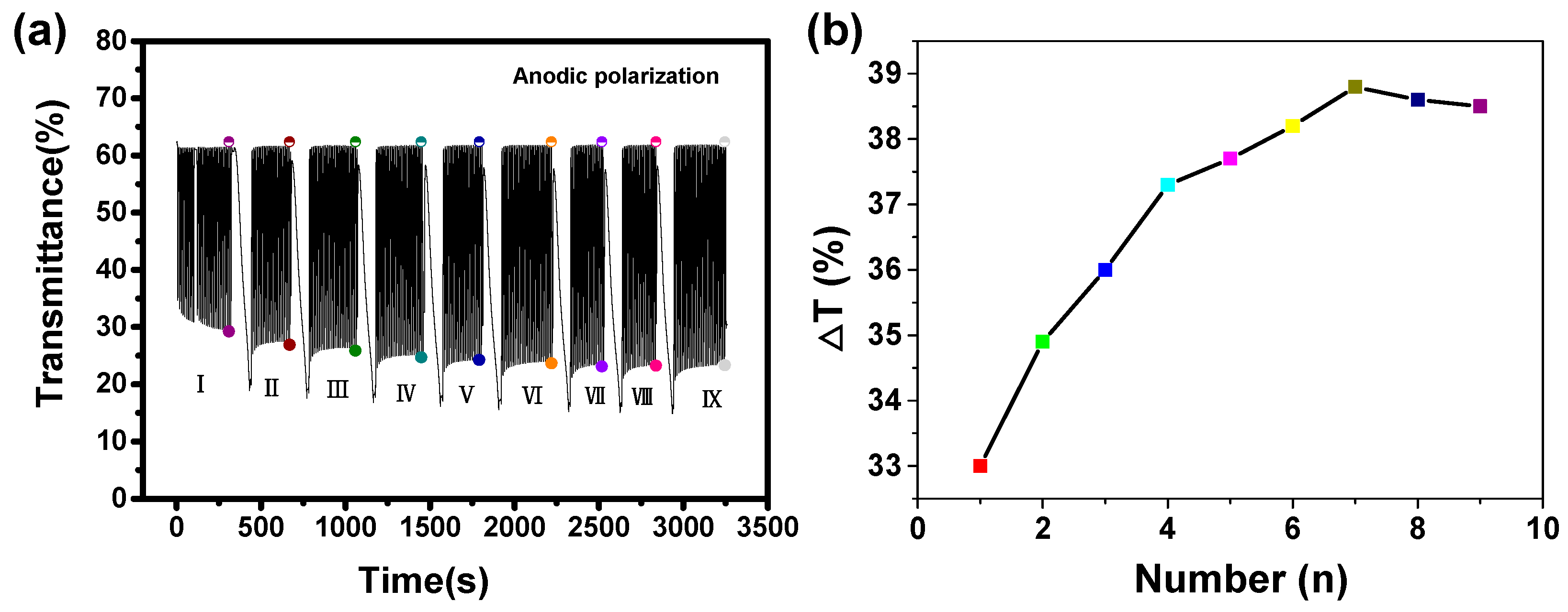
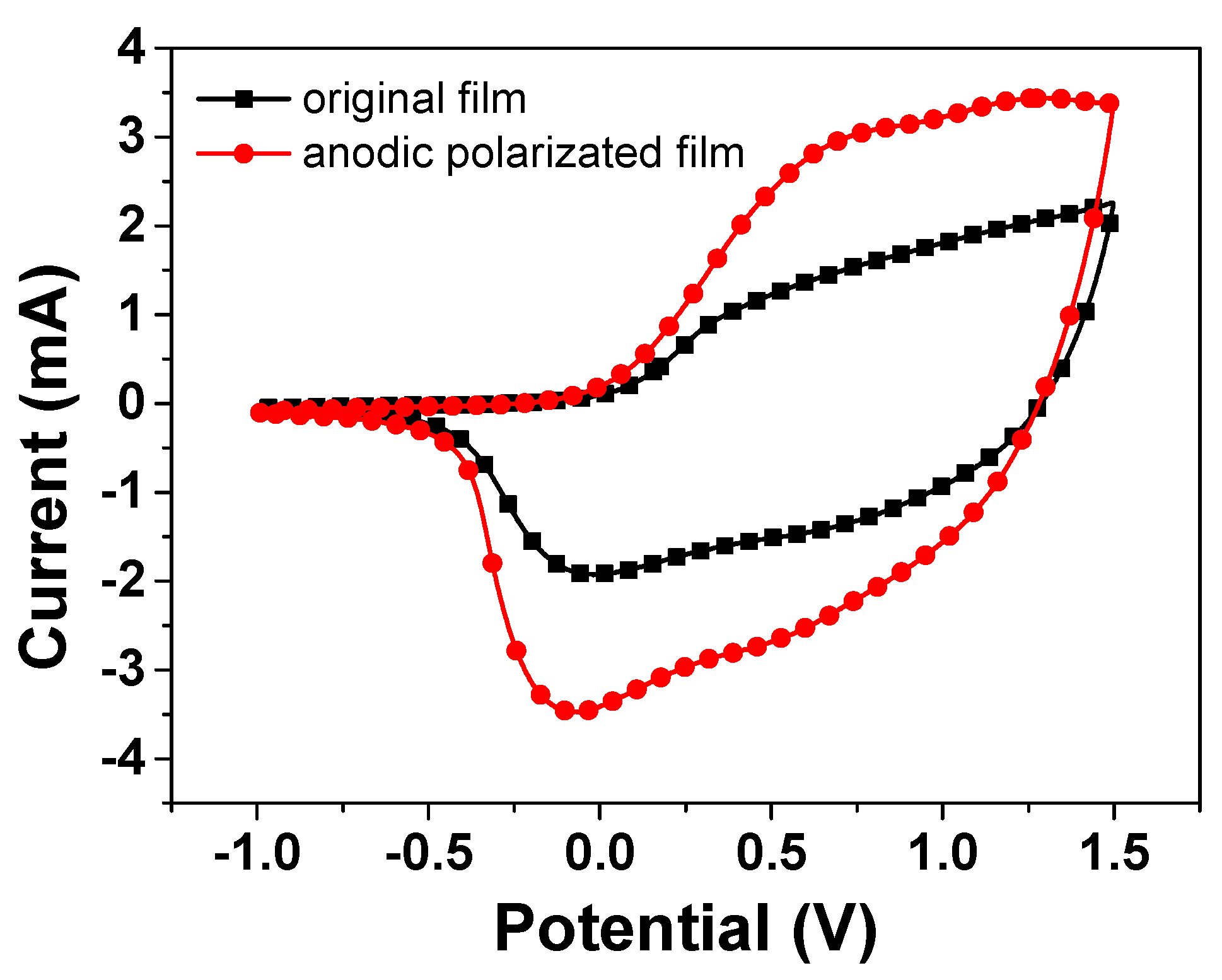
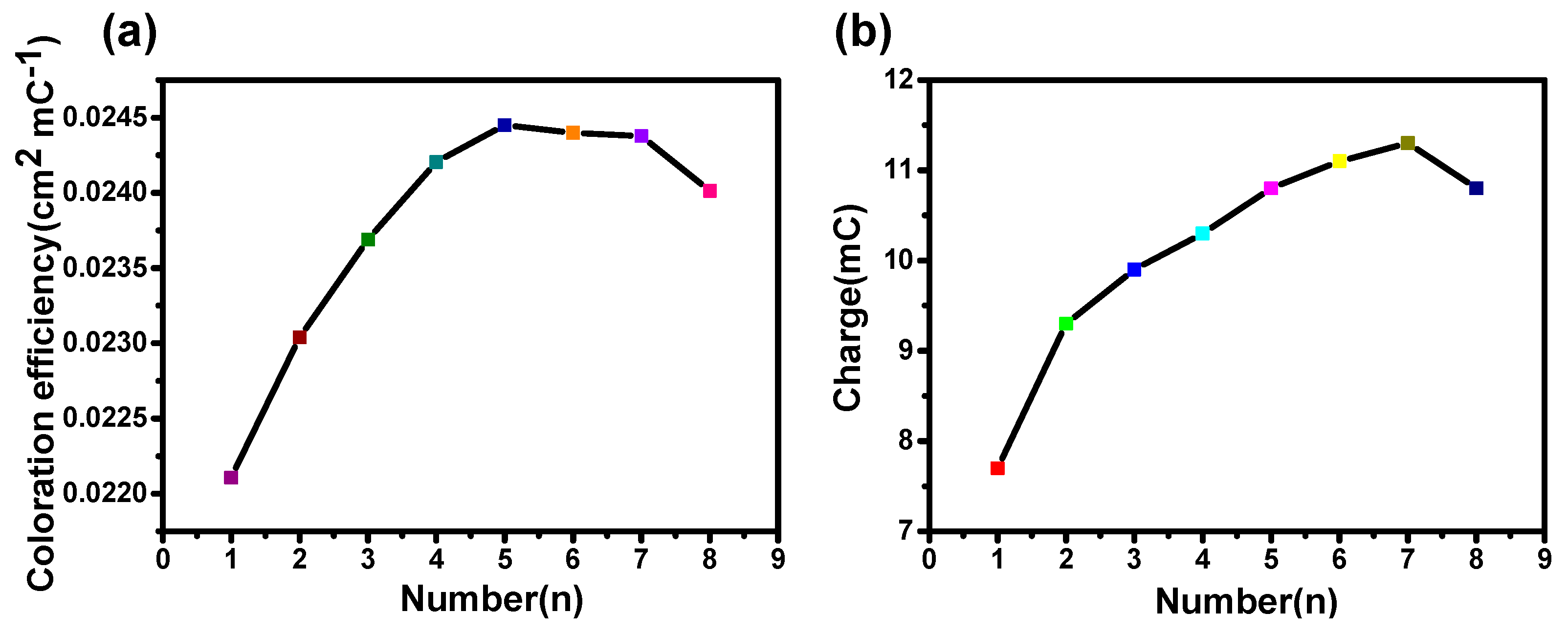
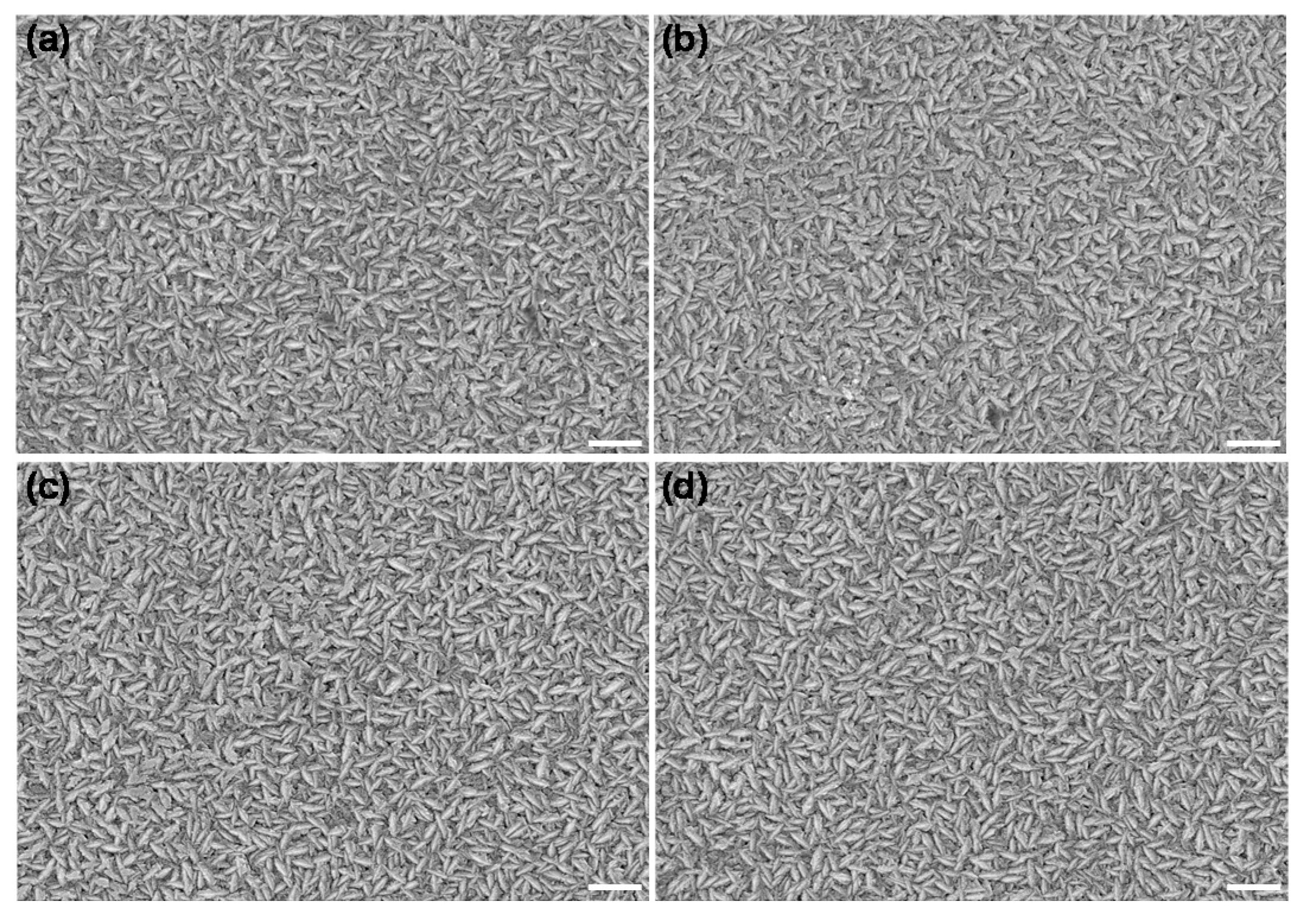
3. Results and Discussion

Figure 1a presents the transmittances at 550 nm of the NiO films with different anodic polarization times (corresponding digital photos are shown in Figure S2). In addition, transmittance spectra of the film in the full visible region in its oxidized and reduced states is shown in Figure S3. In the colored state, all the polarized films have lower transmittance than that of the bleached state. The transmission modulation, ΔT (Tbleached − Tcolored) at 550 nm for the films shown in Figure 1b, indicates that the ΔT value increases from the first anodic polarization to the seventh anodic polarization, and then slightly decreases upon further treatment. The main contribution of the increased transmission modulation is by lowering the transmittance of the colored state. This is because the anodic polarization forces some Ni species that were originally bound by other atoms to be exposed to interact with subsequent Li+ and ClO4 ions, thereby enhancing the modulation ability.
Next, we discuss how the above-mentioned reaction routes can enhance the electrochromic performance after the treatment of the anodic polarization. CV was performed on the NiO film in the potential range from −1.0 to 1.5 V at ν = 30 mV/s. It is generally believed that capacity of the films possesses a larger integral area of the CV curve, representing better EC properties due to the large exchange charge [20]. Figure 2 shows that the CV cycle curve of the anodic polarized film (line in red) can enlarge the integral area of the CV curve compared with the original film. The Ni2+ species in the film would be further oxidized into Ni3+ species by anodic polarization. These newly generated high-valence oxide species are then lithiated in subsequent CV cycles, consequently resulting in the enlargement of the CV area. It is estimated that the quantity of redox charge involved increases by ∼43.8% after the fifth anodic polarization. This evolution is consistent with the corresponding optical responses in Figure 1. These results further prove that the anodic polarization treatment is a simple but useful approach to improve the EC performance, thereby promoting the film’s industrial application.
To further evaluate the electrochromic performance, the coloration efficiency (CE) of the film is presented in Figure 3. The coloration efficiency (CE) is defined as [21]:
CE = ΔOD/Qin
Figure 3a shows that the anodic polarization treatment can significantly improve the CE of the NiO films. The CE can increase from 22.1 cm2/C (the first anodic polarization) to a maximum value of 24.5 cm2/C (the fifth anodic polarization), and then decreases slightly with an increase in anodic polarization time. This indicates that the facile anodic treatment can obtain better EC performance. Moreover, as shown in Figure 3b, the change of capacitance is consistent with the trend in coloration efficiency, proving the additional intercalation during the treatment of anodic polarization can improve the EC performance slightly. This moderate performance improvement drove us to further clarify the possible internal mechanism via a microscopic to study the crystallization properties of materials and their surface structure.
The surface morphology of different NiO films was examined by a SEM operating at 20 kV. The sample surface and cross-section were coated with gold by sputtering prior to introduction into the SEM chamber. Figure 4 shows that the samples with and without polarization treatment both show a regular grain shape and uniformly dense NiO particles without obvious cracks, indicating the polarization treatment had little effect on the surface structure. In particular, as shown in the cross-section images (Figure S4), the NiO films obtained by the E-beam evaporation method exhibit columnar-like crystals, endowing them with a larger specific surface area than that prepared by other methods such as magnetron sputtering [22]. The large surface morphology is due to more reactive sites, which can enhance the effect of ion insertion/extraction in the film, thereby improving the coloration efficiency.
The crystallization of NiO at different polarization times and original films was characterized by XRD, and it was found that the unpolarized and polarized NiO are both crystals with fcc-structures. Figure 5a clearly shows the diffraction peaks of ITO and NiO. The peaks of ITO mainly appear in 2θ = 30.5° (222), 50.9° (440), and 60.5° (622), which is consistent with the JCPDS card (65-3170). The diffraction peaks of NiO mainly appear in 2θ = 37.3° (110), 43.3° (200), and 62.9° (220), corresponding to JCPDS card (04-0835) [23]. However, it should be noted that thin and heavily disordered hydrogen-containing species, which are not visible by XRD, normally formed on the NiO grain surface. All of the results indicate that the polarization treatment does not change the fcc-crystal structure. However, the relatively low diffraction intensity of the film polarized eight times compared to that of others indicates further anodic polarization may damage the NiO film. This hypothesis is also supported by the relatively low optical modulation in Figure 1b and coloration efficiency in Figure 3. As shown in Figure 5b, a shift of the diffraction peak of NiO (220) plane is visible, indicating that stress is present as a result of the anodic polarization. The shift can also be detected for the (200) diffraction peak (Figure S5). As noted, there are hydroxides on the surface of NiO in the initial state, and treatment will decompose or transform these hydroxides into other species. The following processes would occur at the initial anodic polarizations where the positive ions are removed and negative ions are absorbed at the Ni sites:
Ni(OH)2 ↔ NiOOH + H+ + e
Ni(OH)2 + OH ↔ NiOOH + H2O+e
NiO + ClO4 ↔ NiO•ClO4 (absorbed)
LiyNiO ↔ NiO + yLi+ + ye
The exact portion of each process is unclear; however, it can be noted that an increase in the Ni3+ is inevitable, as shown in Figure 6 from the XPS data. This is discussed below. After anodic polarization four times, a blue shift of the (220) peak indicates the NiO lattice is expanded. This is very likely due to Reaction (1), in which Ni(OH)2 at the NiO grain surface is transformed into NiOOH while releasing the H+. Granqvist et al. also observed a blue shift of the (220) peak when cycling NiO in KOH [24]. As shown in Figure 1, each polarization is performed after 100 CV cycles where Reactions (3) and (4) are dominating during the CV cycling. It has been reported that the shift (220) peak to a high angle is associated with irreversible Li insertion [24,25,26], which is similar to our case in which some Li+ ions are irreversibly staying in the NiO matrix. AFM is employed to investigate the surface roughness and morphology of the NiO films upon cycling and anodic polarization (Figure 7). It can be seen that, although there is no evident change from the SEM images, the micron-structure of the NiO and its surface roughness have significant variation. More specifically, the surface roughness after two anodic polarization treatments increases from 4.51 to 6.87 nm, and more importantly, further CV cycling and anodic polarization treatments gradually reduce its roughness to 6.01 nm. Furthermore, the overall surface morphology changes from a small island structure to a blurrier structure upon cycling and anodic polarization. However, we are unable to distinguish whether cycling or anodic polarization plays a more significant role at the current stage.
The XPS measurement of NiO films was undertaken to confirm the valence state information of NiO films. The O1s XPS spectra of the original and polarized NiO films are shown in Figure S6. O1s states in oxide phases of NiO give two peaks centered at 528.6 and 530.4 eV. The peak at 528.6 eV is ascribed to Ni2+. The peak at 530.4 eV is from the Ni3+ species [27]. In the hydrogen containing phases of (Ni(OH)2)3•2H2O, the O1s peak is located at approximately 532 eV [28,29]. As shown in Figure 7a–d, the peak at approximately 528.6 eV decreases in intensity upon the treatment of polarization. This change of intensity can be attributed to the more Ni3+ active sites exposed in the polarized films. The transformation of nickel oxide to hydroxide may involve the excess oxygen present in the films from the beginning. In addition, the red-shift phenomenon of the two peaks (Figure S7) also confirms the above-mentioned mechanism. On this basis, we calculated the proportion of different valence ions, which is illustrated in the Figure S7. The ratio of Ni2+/Ni3+ changes from 0.516 (original film) to 0.688 (anodic polarization two times), 0.792 (anodic polarization four times), and 0.968 (anodic polarization eight times). This indicates polarized films are suitable for electrochromism due to the presence of an enhanced amount of Ni3+. In addition, the signal of element Cl was also detected from the XPS measurement (Figure 7e), indicating the anodic polarization forces the ClO4- to attach to the Ni sites, which is in very good agreement with Reaction (3). These elemental analysis results further prove that polarization treatment can improve the electrochromic effect of NiO film.

4. Conclusions

In summary, NiO films were fabricated by the E-beam evaporation method, followed by anodic polarization treatment to enhance the EC performance. The optical properties of NiO films as functions of the number of anodic polarizations were systematically investigated. A large optical contrast of 38.8% at 550 nm and high coloration efficiency (24.5 cm2/C) were achieved in the optimized NiO films. XRD, SEM, and XPS were used to characterize the crystallinity, surface structure, and composition, respectively. In addition, the XPS results indicate that anodic polarization can generate more Ni3+ species, which are essential for the improvement of EC performance. Moreover, the lattice stress in NiO films can also have an effect on the improvement of EC properties. This study provides an easy and effective approach to fabrication of NiO films with high EC performance, which is attractive for further commercialization of EC devices.

Supplementary Materials

The following are available online at https://www.mdpi.com/article/10.3390/cryst11060615/s1, Table S1: different paraments included in the process of e-beam evaporation. Figure S1: The specific surface area of NiO films prepared by e-beam evaporation. Figure S2: The photograph images of NiO films with the original films. Figure S3: Transmittance spectra of NiO thin films in the full visible region. Figure S4: The cross-section images obtained by SEM. The scale bar is 400 nm. Figure S5: The dynamic change of (200) planes during the anodic polarization process. Figure S6: The O1s XPS spectra of the original and polarization-treated NiO films with different times. Figure S7: The percentage of Ni2+ and Ni3+ as functions of anodic polarization numbers.

Author Contributions

X.G. conducted experiments and wrote the draft. X.G., W.W. and R.-T.W. analyzed that data and finalized the manuscript. W.W. and R.-T.W. supervised the project. All authors have read and agreed to the published version of the manuscript.

Funding

This work was financially supported by the Foundation of Chinese Academic of Sciences (Grant No. CXJJ-17-M158).

Data Availability Statement

The data and methods used in the research are presented in sufficient detail in the document for other researchers to replicate the work.

Acknowledgments

The authors gratefully acknowledge the financial support from the Foundation of Chinese Academic of Sciences (Grant No. CXJJ-17-M158).

Conflicts of Interest

The authors declare no conflict of interest.

References

  1. Rosseinsky, D.R.; Mortimer, R.J. Electrochromic systems and the prospects for devices. Adv. Mater. 2010, 13, 783–793. [Google Scholar] [CrossRef]
  2. Lu, N.; Zhang, P.; Zhang, Q.; Qiao, R.; He, Q.; Li, H.-B.; Wang, Y.; Guo, J.; Zhang, D.; Duan, Z.; et al. Electric-field control of tri-state phase transformation with a selective dual-ion switch. Nature 2017, 546, 124–128. [Google Scholar] [CrossRef] [PubMed] [Green Version]
  3. Wang, C. Electrochromic Nanocrystal Quantum Dots. Science 2001, 291, 2390–2392. [Google Scholar] [CrossRef]
  4. Granqvist, C.-G. Electrochromic materials: Out of a niche. Nat. Mater. 2006, 5, 89–90. [Google Scholar] [CrossRef]
  5. Mortimer, R.J. Electrochromic Materials. Annu. Rev. Mater. Res. 2011, 41, 241–268. [Google Scholar] [CrossRef]
  6. Hassab, S.; Shen, D.E.; Österholm, A.M.; Rocha, M.D.; Song, G.; Alesanco, Y. A new standard method to calculate electro-chromic switching time. Sol. Energy Mater. Sol. Cells 2018, 185, 54–60. [Google Scholar] [CrossRef]
  7. Chandrasekhar, P.; Zay, B.J.; Birur, G.C.; Rawal, S.; Pierson, E.A.; Kauder, L.; Swanson, T. Large, Switchable electrochromism in the visible through far-infrared in conducting polymer devices. Adv. Funct. Mater. 2002, 12, 95–103. [Google Scholar] [CrossRef]
  8. Cui, B.-B.; Zhong, Y.-W.; Yao, J. Three-State Near-Infrared Electrochromism at the Molecular Scale. J. Am. Chem. Soc. 2015, 137, 4058–4061. [Google Scholar] [CrossRef]
  9. Monk, P.M.S.; Mortimer, R.J.; Rosseinsky, D.R. Electrochromism: Fundamentals and Applications; John Wiley & Sons: Hoboken, NJ, USA, 2007. [Google Scholar]
  10. Granqvist, C. Handbook of Inorganic Electrochromic Materials; Elsevier: Amsterdam, The Netherlands, 1995. [Google Scholar]
  11. Seidel, J.; Luo, W.; Suresha, S.J.; Nguyen, P.K.; Lee, A.S.; Kim, S.Y.; Yang, C.H.; Pennycook, S.J.; Pantelides, S.T.; Scott, J.F. Prominent electrochromism through vacancy-order melting in a complex oxide. Nat. Commun. 2012, 3, 1–6. [Google Scholar] [CrossRef]
  12. Zheng, H.; Ou, J.Z.; Strano, M.S.; Kaner, R.B.; Mitchell, A.; Kalantar-Zadeh, K. Nanostructured tungsten oxide-properties, syn-thesis, and applications. Adv. Funct. Mater. 2011, 21, 2175–2196. [Google Scholar] [CrossRef]
  13. Faria, I.C.; Kleinke, M.; Gorenstein, A.; Fantini, M.C.A.; Tabacniks, M.H. Toward Efficient Electrochromic NiO x Films: A Study of Microstructure, Morphology, and Stoichiometry of Radio Frequency Sputtered Films. J. Electrochem. Soc. 1998, 145, 235–240. [Google Scholar] [CrossRef]
  14. Browne, M.P.; Nolan, H.; Berner, N.C.; Duesberg, G.S.; Lyons, M.E.G. Electrochromic nickel oxide films for smart window applications. Int. J. Electrochem. Sci. 2016, 11, 6636–6647. [Google Scholar] [CrossRef]
  15. Mihelčič, M.; Vuk, A.Š.; Jerman, I.; Orel, B.; Švegl, F.; Moulki, H.; Faure, C.; Campet, G.; Rougier, A. Comparison of electro-chromic properties of Ni1−xO in lithium and lithium-free aprotic electrolytes: From Ni1−xO pigment coatings to flexible electrochromic devices. Sol. Energy Mater. Sol. Cells 2014, 120, 116–130. [Google Scholar] [CrossRef]
  16. Conell, R.S.; Corrigan, D.A.; Powell, B.R. The electrochromic properties of sputtered nickel oxide films. Sol. Energy Mater. Sol. Cells 1992, 25, 301–313. [Google Scholar] [CrossRef]
  17. Vidales-Hurtado, M.A.; Mendoza-Galván, A. Optical and structural characterization of nickel oxide-based thin films obtained by chemical bath deposition. Mater. Chem. Phys. 2008, 107, 33–38. [Google Scholar] [CrossRef]
  18. Passerini, S.; Scrosati, B.; Gorenstein, A. The Intercalation of Lithium in Nickel Oxide and Its Electrochromic Properties. J. Electrochem. Soc. 1990, 137, 3297–3300. [Google Scholar] [CrossRef] [Green Version]
  19. Sahu, D.; Wu, T.-J.; Wang, S.-C.; Huang, J.-L. Electrochromic behavior of NiO film prepared by e-beam evaporation. J. Sci. Adv. Mater. Devices 2017, 2, 225–232. [Google Scholar] [CrossRef]
  20. Yang, P.; Li, L.; Yu, S.; Zheng, H.; Peng, W. The annealing temperature and films thickness effect on the surface morphology, preferential orientation and dielectric property of NiO films. Appl. Surf. Sci. 2019, 493, 396–403. [Google Scholar] [CrossRef]
  21. Vernardou, D.; Psifis, K.; Louloudakis, D.; Papadimitropoulos, G.; Davazoglou, D.; Katsarakis, N.; Koudoumas, E.; Koudoumas, E. Low Pressure CVD of Electrochromic WO3 at 400 °C. J. Electrochem. Soc. 2015, 162, H579–H582. [Google Scholar] [CrossRef]
  22. Lee, S.J.; Lee, T.G.; Nahm, S.; Kim, D.H.; Han, S.H. Investigation of all-solid-state electrochromic devices with durability en-hanced tungsten-doped nickel oxide as a counter electrode. J. Alloys Compds. 2019, 815, 152399–152402. [Google Scholar] [CrossRef]
  23. Bouessay, I.; Rougier, A.; Beaudoin, B.; Leriche, J. Pulsed Laser-Deposited nickel oxide thin films as electrochromic anodic materials. Appl. Surf. Sci. 2002, 186, 490–495. [Google Scholar] [CrossRef]
  24. Wen, R.T.; Niklasson, G.A.; Granqvist, C.G. Electrochromic nickel oxide films and their compatibility with potassium hydroxide and lithium perchlorate in propylene carbonate: Optical, electrochemical and stress-related properties. Thin Solid Films 2014, 565, 128–135. [Google Scholar] [CrossRef] [Green Version]
  25. Kubo, T.; Nishikitani, Y.; Sawai, Y.; Iwanaga, H.; Sato, Y.; Shigesato, Y. Electrochromic properties of LixNiyO films deposited by RF magnetron sputtering. J. Electrochem. Soc. 2009, 156, H629–H633. [Google Scholar] [CrossRef]
  26. Moulki, H.; Park, D.H.; Min, B.K.; Kwon, H.; Hwang, S.J.; Choy, J.H.; Toupance, T.; Campet, G.; Rougier, A. Improved electro-chromic performances of NiO based thin films by lithium addition: From single layers to devices. Electrochim. Acta 2012, 74, 46–52. [Google Scholar] [CrossRef]
  27. Uhlenbrock, S.; Scharfschwerdt, C.; Neumann, M.; Illing, G.; Freund, H.-J. The influence of defects on the Ni 2p and O 1s XPS of NiO. J. Phys. Condens. Matter 1992, 4, 7973–7978. [Google Scholar] [CrossRef]
  28. Wu, Y.; Wu, G.; Ni, X.; Wu, X. Structural, infrared, x-ray photoelectron, and Raman spectral characterization of electrochromic nickel oxide films. In Proceedings of the Fourth International Conference on Thin Film Physics and Applications, Shanghai, China, 8–11 May 2000; Volume 4086, pp. 418–423. [Google Scholar] [CrossRef]
  29. Ahn, K.S.; Nah, Y.C.; Sung, Y.E. Surface morphological, microstructural, and electrochromic properties of short-range ordered and crystalline nickel oxide thin films. Appl. Surf. Sci. 2002, 199, 259–269. [Google Scholar] [CrossRef]
Figure 1. (a) Comparison of in situ optical response at 550 nm of the same NiO film as a function of the anodic polarization time under the same CV test conditions: in the range from −1.0 to 1.5 V at υ = 30 mV/s in PC−LiClO4. (b) Corresponding transmittance changes (ΔT) under different conditions.
Crystals 11 00615 g001
Figure 2. Cyclic voltammograms of the NiO films at different working current during different operation conditions: in the range from -1.0 to 1.5 V at υ = 30 mV/s in PC−LiClO4.
Crystals 11 00615 g002
Figure 3. (a) Coloration efficiency of NiO films as a function of different anodic polarization times. (b) Corresponding charge with different anodic polarization times.
Crystals 11 00615 g003
Figure 4. SEM morphology of NiO films with the original films (a) and different times of anodic polarization: two times (b), four times (c), and eight times (d). All scale bars are 400 nm.
Crystals 11 00615 g004
Figure 5. (a) XRD patterns of NiO films in original state and different anodic polarization times. (b) The dynamic change of (220) planes during the anodic polarization process.
Crystals 11 00615 g005
Figure 6. O1s XPS spectra of NiO films in the original films (a) and different times of anodic polarization: two times (b), four times (c), and eight times (d). (e) Cl2p XPS spectra of NiO films in the original films and different times of anodic polarization: two times, four times, and eight times.
Crystals 11 00615 g006
Figure 7. AFM morphology of NiO films with the original films (a) and different times of anodic polarization: two times (b), four times (c), and eight times (d).
Crystals 11 00615 g007
Publisher’s Note: MDPI stays neutral with regard to jurisdictional claims in published maps and institutional affiliations.

