Abstract
III-Nitride semiconductors are the materials of choice for state-of-the-art opto-electronic and high-power electronic applications. Through the incorporation of magnetic ions, like transition metals and rare-earths, III-Nitrides have further extended their applicability to spintronic devices. However, in most III-Nitrides the low solubility of the magnetic ions leads to the formation of secondary phases that are often responsible for the observed magnetic behavior of the layers. The present review summarizes the research dedicated to the understanding of the basic properties, from the fabrication to the performance, of III-Nitride-based phase-separated magnetic systems containing embedded magnetic nanostructures as suitable candidates for spintronics applications.
1. Introduction
The birth of spin-electronics or spintronics, which aims at exploiting not only the charge of the electron but also its spin, occurred with the discovery of the giant magnetoresistance effect [1,2]. This effect has since set the basis for the development of faster and more efficient magnetic recording media. However, the non-compatibility of metals with the constantly growing Si-technology due to their high impedance mismatch, prompted an urge for new materials with tunable material properties. The most promising candidates have been magnetic semiconductors, also called dilute magnetic semiconductors (DMS) [3,4]. The field of research of DMS has been already active for about five decades and is based on the addition of magnetic ions to technologically important semiconductors, in order to exploit the semiconducting properties, like the tunable band gap, and at the same time adding a magnetic moment [5].
The very first studies concerning magnetic semiconductors focused on II-VI semiconductors, such as CdTe and ZnSe, where the valence of the cation matches that of the Mn used as the magnetic impurity. However, the low electric n and p doping efficiency in these materials limited their applicability. Concerning the III-V semiconductors, GaAs doped with Mn has been the most studied magnetic semiconductor, where hole-mediated ferromagnetism [5] and electrical-field manipulation of the magnetization [6] was achieved. However, despite large efforts the Curie Temperature () for this magnetic semiconductor still lies below room temperature (RT) [7].
In the year 2000 Dietl et al. predicted that carrier-mediated ferromagnetism could be achieved in two wide-band gap semiconductors: Co-doped ZnO and Mn-doped GaN when doped with a magnetic dopant concentration above 5% and enough free holes to mediate the magnetic interaction between the ions [8]. However, the low solubility limit of the magnetic ions in these two semiconducting materials made it soon evident that the realization of a DMS with above RT was more challenging than expected, paving the way for the investigation of the so-called condensed magnetic semiconductors (CMS) [9]. The incorporation of the magnetic ions in a semiconductor depend on the growth conditions: either they substitute the original lattice cations and are randomly distributed in the semiconducting matrix in a DMS [10], or they aggregate into regions in the semiconducting matrix leading to crystallographic and/or chemical phase separation in a CMS [9,11]. These phase-separated materials are expected to provide an efficient, robust and energy-saving platform in particular for magnetic data storage and generation of polarized spin currents [12]. Further applications, include the spin current injection into the semiconductor host crystal through spin pumping, and spin current detection by inverse spin Hall effect [13], as well as the possibility to study frustrated magnetic systems and spin glass behaviors [14].
The incorporation of magnetic ions like transition metals (TM) and rare-earths (RE) in III-Nitrides has been widely studied [15,16,17]. Theoretical ab initio calculations have predicted that TM-doped dilute GaN-based semiconductors could further serve as antiferromagnetic semiconductors, taking advantages of a 100% spin polarization but zero net magnetic moment [18]. For both dilute and condensed magnetic III-Nitrides, the observation of RT ferromagnetisms has been reported [15]. In many cases, the observed ferromagnetic signatures are attributed to the formation of secondary phases consisting of compounds, where X represents a TM or RE ion. A first-principle density functional theory-generalized gradient approximation study of the TM doping of bulk GaN and the nearest neighbor interactions at the (0001) GaN surfaces, predicted that Fe ions tend to aggregate at surfaces, while Cr and Mn tend to repulse each other [19].
In the present work the continous progress dedicated to the understanding of the basic properties, from the fabrication to the performance, of phase-separated III-Nitride-based magnetic systems containing embedded magnetic nanostructures is presented and summarized. The review is divided into four main sections dedicated to the different III-Nitride CMS: (i) Mn-doped GaN, (ii) Fe-doped GaN, (iii) Cr-doped AlN and GaN, and (iv) Gd-doped GaN. For each material system, the different growth methods employed for fabricating the phase-separated layers, the structural properties of the secondary phases and the corresponding magnetic properties of the layers, are presented. At the end of each section a brief summary of the magnetic phases present in the III-Nitride CMS is provided. Many similarities between the embedded magnetic nanostructures in the different material systems and the employed growth mode are identified. It is found that the embedded magnetic nanostructures can be often tuned on demand by adjusting the fabrication conditions and depend largely on the growth mode and growth method employed, leading to the self-assembly of magnetic nanostructures. This work underlines the importance of a detailed nanocharacterization in these CMS and demonstrates the huge potential of these technologically relevant III-Nitride CMS for their implementation into spintronic devices.
2. Mn-Doped GaN
Manganese-doped GaN is a very controversial magnetic semiconductor with values reported between 4.5 K [20] to 940 K [21]. The origin of the high reported is still under debate, mostly concerning the question whether the material is dilute or not [11]. Despite the predictions by Dietl et al. [8], no carrier-mediated magnetism in GaMnN has been so far demonstrated. However, the achievement of a dilute ferromagnetic insulator with Mn concentrations below 10% and ranging from 1.8 K [22] to 10 K [23] has been reported. In these materials the ferromagnetism is well-described by tight-binding and Monte Carlo simulations in the frame of a superexchange scenario with Jahn Teller distortions of the dilute Mn ions [22,24]. Antiferromagnetic interactions in GaMnN have been also reported for samples containing between 10% [25] and 36% [26] of Mn ions attributed to a majority of the ions being in the Mn charge state.
2.1. (Ga)MnN Embedded Magnetic Nanoclusters in GaN
The solubility limit of Mn in hexagonal GaN was calculated based on phase equilibrium calculations and thermodynamic analysis constructed Ga-Mn-N phase diagrams [27]. Additional ab initio electronic structure calculations were employed to estimate the formation enthalpies of the binary and ternary secondary phases. It was found that the ternary GaMnN is the most stable phase likely to form in GaMnN systems grown under low pressure conditions like molecular beam epitaxy (MBE) and metal-organic vapour phase epitaxy (MOVPE). In fact a solubility of up to 2.4% of Mn in the wurtzite GaMnN was predicted for growth temperatures taking place at 1073 K.
The first observation of phase-decomposition was reported by Zajac. et al. in microcrystalline GaMnN layers [25]. These were fabricated by the ammonothermal technique with a Mn concentration of 0.5%. The secondary phase was identified as crystalline MnN from x-ray diffraction (XRD) and from the XRD intensity, it was estimated that only 5% of the entire layer volume was occupied by the nanoclusters. The layers presented a dominant paramagnetic behavior due to the dilute Mn ions substituting for the Ga cations in the GaN matrix with spin S = 5/2. Additionally, a linear component associated to the MnN nanocrystals was observed, which is consistent with MnN being antiferromagnetic with a Néel Temperature () of 925 K [28], shown in Figure 1.
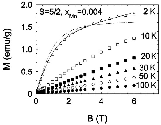
Figure 1.
Magnetization of a GaMnN layer with 0.4% Mn acquired at different temperatures. The dashed line fit to the data at 2 K is for pure Brillouin paramagnetism and the solid line is the Brillouin and an additional antiferromagnetic component attributed to the MnN nanoclusters. Reproduced with permission from Reference [25].
The same group reported the formation of numerous MnN phases with and in GaMnN obtained from a detailed analysis of the contributions observed in the magnetometry measurements and the separate fabrication of MnN phases by adjusting the ammonia flow and the growth temperature during the ammonothermal process [29]. They described the magnetic properties of their GaMnN layers as a contribution of several components: (i) a Brillouin-like paramagnetic component from the Mn diluted in the GaN matrix, and (ii) a ferromagnetic or antiferromagnetic contribution attributed to the MnN nanocrystallites in the layers. Depending on the employed fabrication conditions, they were able to corroborate the formation of antiferromagnetic MnN ( = 650 K) [30], antiferromagnetic MnN and ferrimagnetic MnN ( = 790 K) [31] in their GaMnN layers. They concluded that according to their findings, the presence of MnN phases could not be excluded solely from the results obtained from conventional XRD techniques, as the volume of these phases in the layers was sometimes below the detection limit.
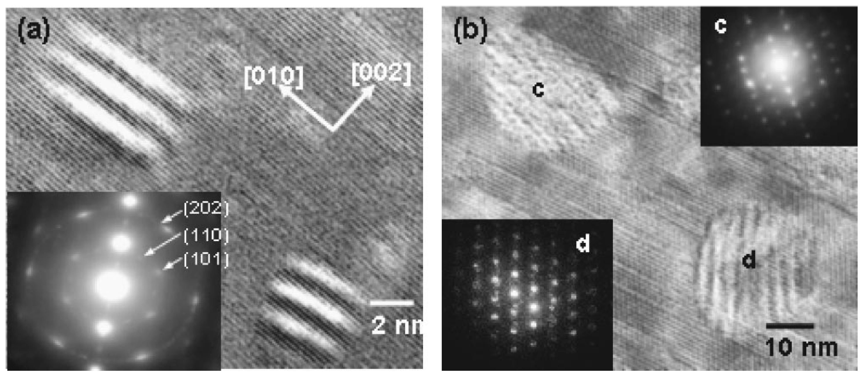
The formation of MnN, MnGa and MnN nanoclusters was further identified in Mn-implanted p-type GaN layers by high-resolution transmission electron microscopy (HRTEM) [32]. The p-type GaN templates with a hole carrier concentration of cm grown by metalorganic chemical deposition on a (0001) sapphire substrate were implanted with Mn ions up to a concentration of 5% and subsequently annealed for 30 s to temperatures of 700 °C to 900 °C. Depending on the annealing temperature, the formation of different nanoclusters were observed by HRTEM and corresponding selected area diffraction patterns (SADPs) as seen in Figure 2.

Figure 2.
Identification of secondary phases in Mn-implanted GaN by high-resolution transmission electron micorscopy (HRTEM) imaging and selected area diffraction patterns (SADPs) annealed at: (a) 700 °C with the identified MnGa phase, and (b) 900 °C with the phases identified as MnN (b)-c and MnN (b)-d, respectively. Reproduced with permission from Reference [32].
In the Mn-implanted GaN layers annealed below 800 °C the formation of Mn3Ga nanoclusters with sizes ranging between 3 nm and 7 nm were identified from SADPs. The magnetization of these layers showed a weak ferromagnetic behavior associated to the Mn3Ga nanoclusters, for which a weak ferromagnetic behavior in the hexagonal phase [33] and a ferrimagnetic behavior in the tetragonal crystal structure [34] have been reported. When the implanted layers were annealed at temperatures above 900 °C, the nanoclusters size increased to around 30 nm and the phases were identified as MnN and MnN, both phases are antiferromagnetic with above RT [28,35], leading to a reduction in the magnetization of the layers.
The formation of Mn3Ga in Mn-implanted layers has been underlined by the work of Sun et al., where ferromagnetic signatures accompanied by a magnetic anisotropy was attributed to the formation of Mn3Ga secondary phases in Mn-implanted nonpolar GaN annealed to 900 °C [36]. The magnetic anisotropy suggests two contributions responsible for the net magnetic moment: (i) the Mn ions diluted in the GaN matrix, and (ii) polarization induced changes in the enviroment of the magnetic ions. Recently, an inverse polatization effect in dilute (Ga,Mn)N layers grown by MOVPE induced by an applied electric field demonstrated the control over the anisotropy of the Mn3+ ions in the GaN matrix [37].
While the formation of MnN secondary phases was observed in layers prepared by the ammonothermal technique and ion implantation, the formation of perovskite GaMnN was reported in layers grown by MBE on different substrates for Mn concentrations above 2% [38,39,40,41]. The GaMnN phase is expected to be ferromagnetic near its equilibrium volume and is expected to have a large spin polarization of about 60% [42], while a spin-glass behavior at temperatures below 133 K has been experimentally reported for the antiperovskite crystalline structure [43]. The GaMnN layers containing GaMnN secondary phases show a ferromagnetic component with a = 175 K, which is not directly assigned to the embedded phases.
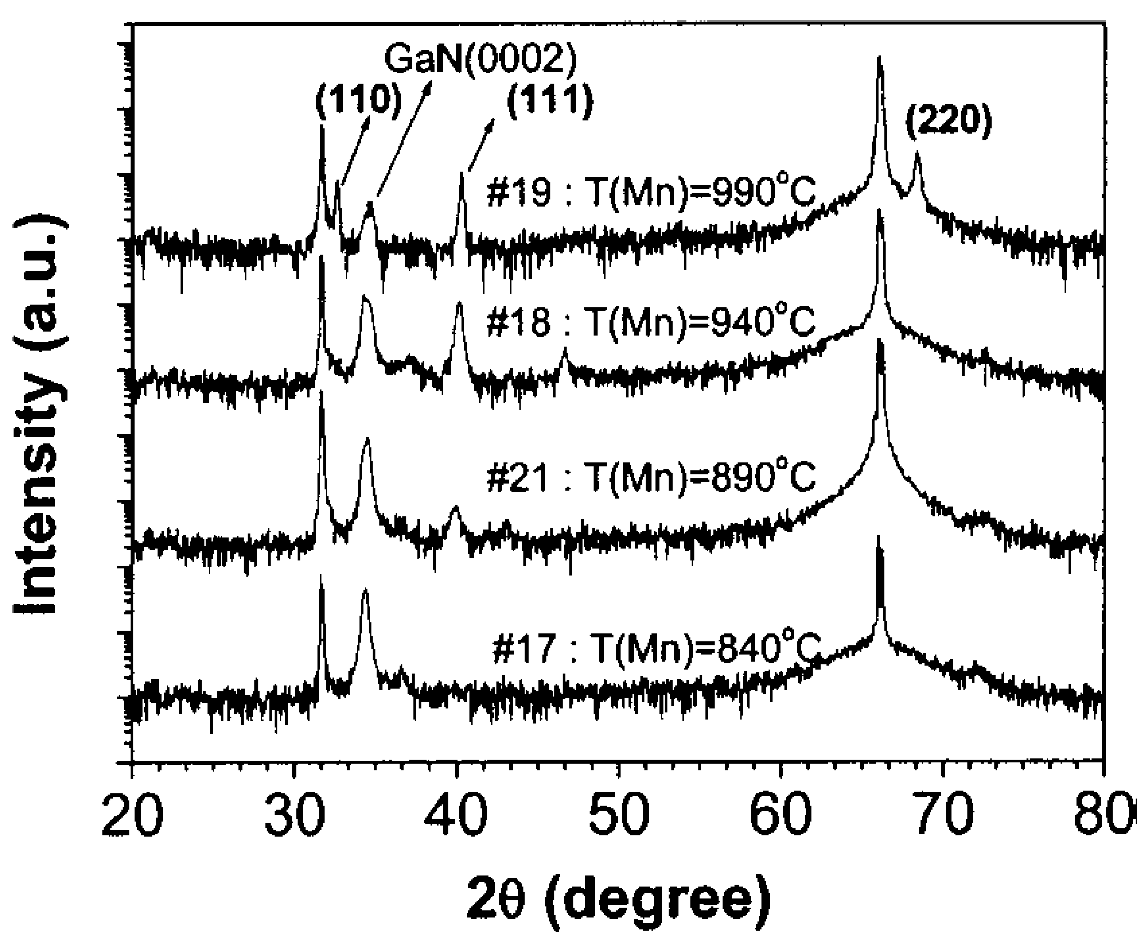
The GaMnN precipitates in p-type GaMnN layers, identified from XRD presented in Figure 3, exhibit a slightly larger of 200 K and enhance the conduction in the layers, leading to an anomalous Hall effect at RT [38]. This is an unexpected behavior, taking into consideration that MnAs precipitates in (Ga,Mn)As are known to increase the resistivity of the layers [44]. The increased conductivity is explained in the frame of the formation of an ohmic contact between the GaMnN precipitates and the surrounding GaMnN matrix leading to an enhanced conduction, proving the suitability of this phase-separated material for magnetotransport devices.

Figure 3.
Molecular beam epitaxy (MBE) grown GaMnN layers containing embedded GaMnN nanocrystals identified from the (111) diffraction peak measured by X-ray diffraction (XRD). Reproduced with permission from Reference [38].
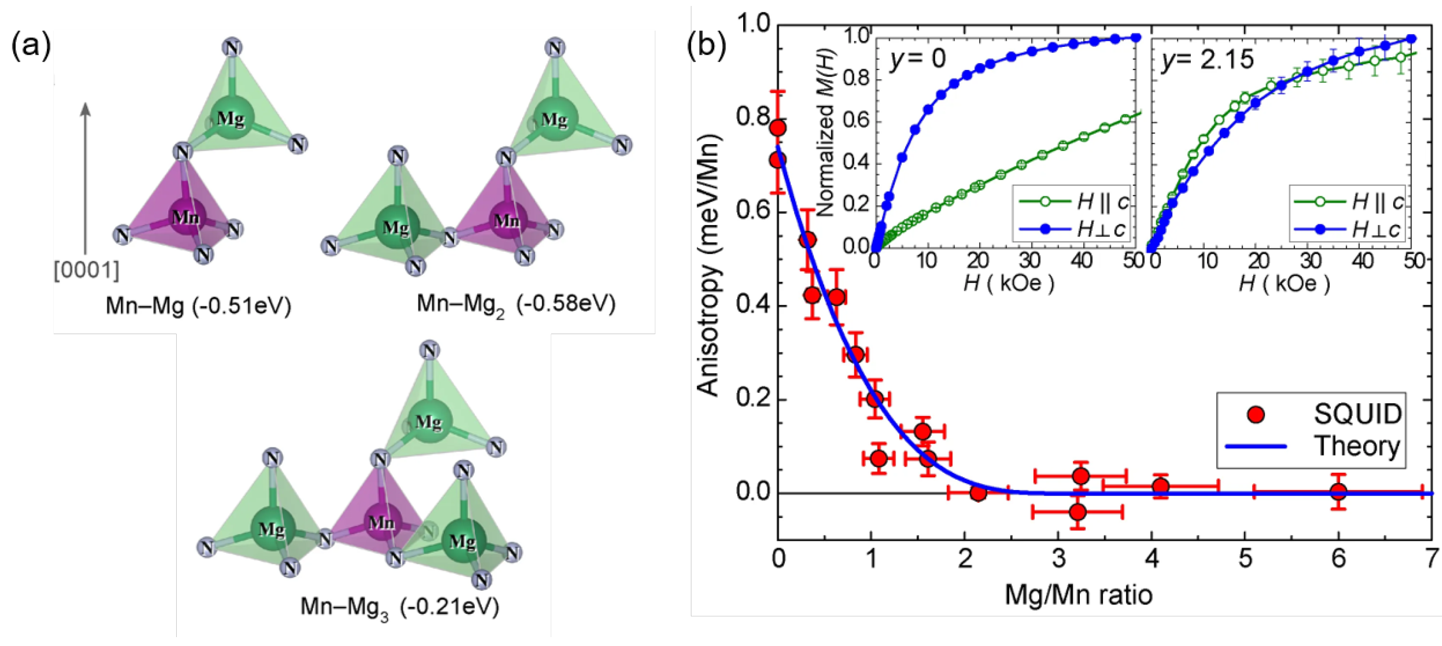
In Mg co-doped GaMnN layers grown by MOVPE, the addition of Mg to provide free holes did not lead to the expected carrier mediated ferromagnetism, but to the formation of Mn-Mg magnetic complexes with tunable spin properties, emitting in the technologically important range of 1.2 m [45,46,47]. Extended x-ray fine structure (EXAFS) and Raman spectroscopy aided the identification of the Mn-Mg complexes with , where k can de adjusted via the fabrication conditions [45,46]. In this way, the co-doping of Mg of GaMnN allows controlling the charge state of the Mn ions and its spin state, as evidenced through ab-initio calculations and superconducting quantum interference (SQUID) measurements, depicted in Figure 4. This is directly evidenced from the magnetic anisotropy of the non-interacting Mn ions shown in the left inset of Figure 4 b. After the addition of Mg, the magnetic anisotropy is strongly reduced, pointing to a reduction in the charge state from Mn to Mn [48]. The strong emission in the infrared of the Mn-Mg complexes in GaN make this material relevant for laser and telecommunication technologies [49].
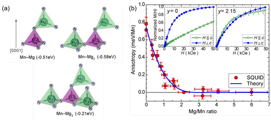
Figure 4.
Tunable spin Mn-Mg complexes in GaMnN grown by MOVPE that serve to modify the magnetic anisotropy of the layers: (a) Schematic representation of the complexes, and (b) magnetic anisotropy as a function of Mg/Mn ratio. Adapted from Reference [45].
Secondary phase formation was also observed for InMnN layers grown by MBE with a Mn concentration as low as 1%, where MnN nanoclusters were detected by XRD [50]. Despite the presence of the antiferromagnetic MnN nanoclusters, the layers were only paramagnetic.
2.2. Summary of Secondary Phases Observed in GaMnN Layers
The binary and ternary secondary phases identified in GaMnN are summarized in Table 1, where their crystal structure, their lattice parameters, and their magnetic properties are listed. The growth methods employed to fabricate the phase-separated GaMnN layers are also included.

Table 1.
Observed secondary-phases in GaMnN, their structural and magnetic properties, as well as the growth technique employed for the growth of the phase-separated layers.
3. Fe-Doped GaN
The incorporation of Fe into GaN began as a way to make the unintentionally n-type doped GaN grown by MOVPE a semiinsulating material suitable for applications into high-electron mobility transistors (HEMTs) [51,52,53], revealing that a very small amount of Fe (<10 ions/cm) was enough to compensate the n-type background of unintentionally doped GaN. However, the addition of Fe also showed the deterioration of the surface quality of the GaN thin layers due to the seggregation of the Fe ions during in-situ fabrication [54,55]. This drawback damped the interest of the research community in the implementation of GaN:Fe in hetereostructures for electronic devices.
Soon, Fe-doped GaN became an appealing material for achieving a magnetic semiconductor with high . The first reports on ferromagnetic signatures were documented in p-type GaN templates grown by MOVPE ( holes/cm) and implanted with Fe ions. The observed ferromagnetism persisted up to 250 K for a Fe concentration of 3% [56] and in layers with an Fe concentration of 10% a paramagnetic to ferromagnetic transition persisiting above 350 K was reported [57]. In both works, the presence of secondary phases was excluded as the source of the observed ferromagnetism. However, due to the low carrier concentrations present in these implanted p-GaN:Fe layers, carrier-mediated ferromagnetism was also excluded, leaving the origin of the observed high unclear.
3.1. Embedded FeN Magnetic Nanocrystals and Nanoclusters in Fe-Doped GaN
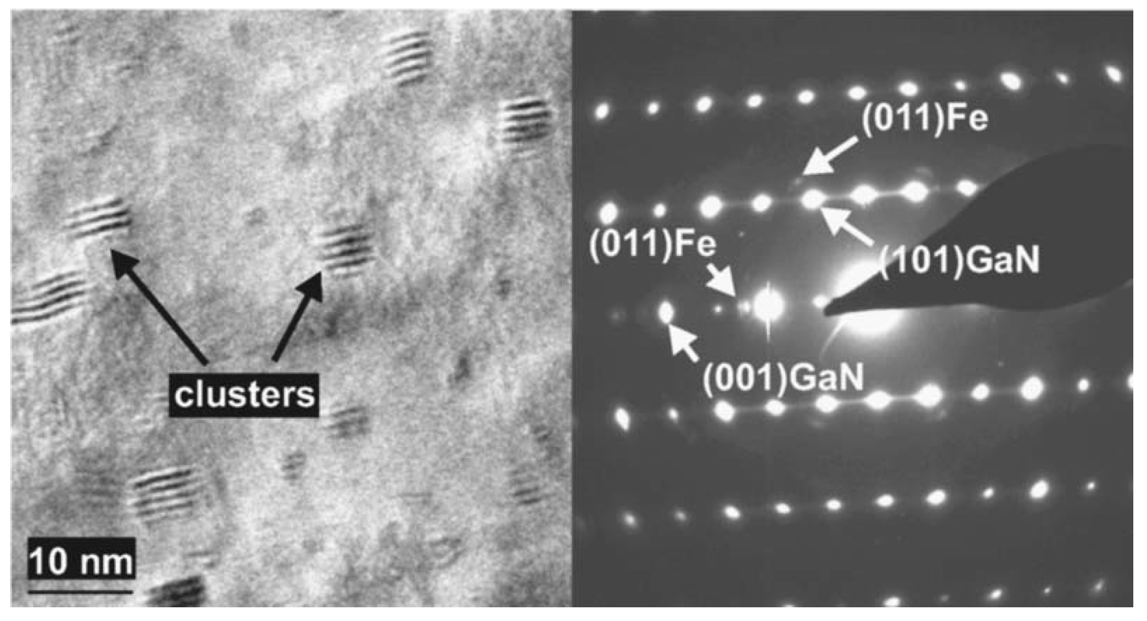
The first observation of phase-decomposition was reported in p-type GaN Fe-implanted samples by Talut et al. [58]. They observed via Mössbauer spectroscopy that the formation of the nanoclusters occurred already during implantation of Fe with a dosis of 4 × cm followed by a 5 min annealing to 850 °C, which was comparable to the dose employed by Shon et al. [57]. The nanoclusters, identified as -Fe, were epitaxially embedded in the GaN matrix with an epitaxial relation (110)(10-11) and (011)(0001), as is seen in the HRTEM micrograph and the corresponding SADP shown in Figure 5. The magnetic properties of these layers displayed a temperature independent paramagnetic Van Vleck contribution assigned to the non-interacting Fe ions and a superparamagnetic behavior consistent with the presence of the Fe nanoclusters. They concluded that not only the fluence, but also the annealing time and annealing temperature in Fe-ion implanted GaN were decisive in the formation and the size of the nanoclusters. So, in order to avoid the phase separation in GaFeN, the recrystallization annealing after implantation should be kept at the lowest temperatures, and should be as short as possible.

Figure 5.
Fe nanoclusters epitaxially embedded in a p-GaN sample after an implantation of 4 Fe ions and subsequently annealed to 800 °C. Left side: HRTEM, and right side: the corresponding SADP. Reproduced with permission from Reference [58].
Further in-situ synchrotron XRD (SXRD) measurements presented in Figure 6 during annealing of the Fe-implanted p-type GaN samples to 1073 K gave a more detailed insight into the formation of the secondary phases [59]. After implantation, the samples do not show any precipitation. However, after annealing to 1073 K a broad diffraction peak assigned to a disordered -FeN phase was observed that turned into an ordered -FeN phase as the sample was cooled down to RT. This process was reversible, but depended on the Fe out-diffusion and gradual oxydation of the Ga and the Fe with each annealing cylce. The temperature dependent measurements of the magnetic moment showed a superparamagnetic behavior pointing at a broad size distribution of the nanoparticles, with an estimated average size of 16 nm. The magnetic moment of the Fe ions was estimated to be 20 times lower than for pure -FeN, indicating that not all the implanted Fe incorporated into the nanoparticles.

Figure 6.
In-situ SXRD (SXRD) observation of the formation of nanoclusters in Fe-implanted p-GaN with a dose of: (a) 8 ions/cm, and (b) 16 ions/cm. Reproduced with permission from Reference [60].
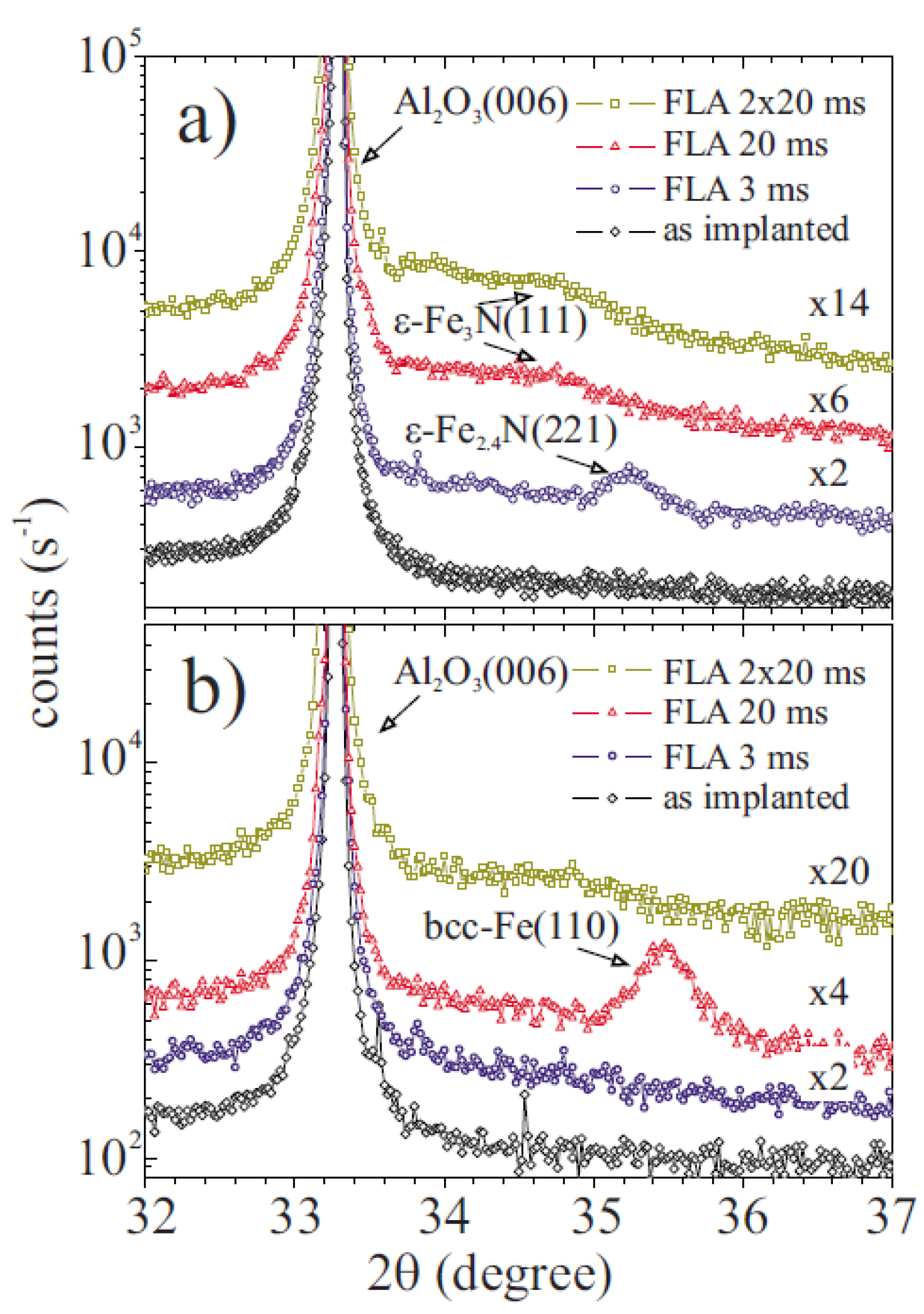
A detailed investigation comparing two different fluences, 8 and 16 cm corresponding to about 9% and 18% at. Fe, and short annealing times by employing flash-light annealing (FLA) during in-situ SXRD demonstrated the formation of secondary phases even at very short annealing times [60]. The correlation of the structural and magnetic properties through Mössbauer spectroscopy, Rutherford back scattering, in-stu SXRD and SQUID magnetometry, allowed identifying spinodal decomposition [11,61] as a preliminary stage before the formation of nanoparticles in Fe-implanted p-type GaN, this being responsible for the complex magnetic interaction observed in the samples. The presence of ferromagnetic signatures was observed only for the annealed samples and was therefore, attributed to the identified -Fe and -FeN nanoparticles formed during the annealing process.
In the case of Fe-doped GaN grown by MOVPE, a detailed characterization at the nanoscale employing a combination of EXAFS, electron paramagnetic resonance, HRTEM, SXRD and SQUID magnetometry demonstrated that the low solubility limit of Fe in GaN leads to the formation of predominantly hexagonal -FeN ferromagnetic oblate nanocrystals (NCs) with a size of (20 ± 2) nm perfectly embedded into the GaN matrix, responsible for the observed high of 540 K [62]. When the GaFeN layers were fabricated in a continous growth mode, a solubility limit of 0.4% of Fe ions into GaN led to the chemical and crystallographic phase separation. The layers containing less than 0.4% Fe ions showed a Brillouin-like paramagnetism associated to the Fe ions in the Fe charge state substituting for the Ga cations, responsible for a p-d exchange interaction in the strong coupling limit [63]. Above the solubility limit, the magnetic properties of the layers displayed two contributions: (i) a paramagnetic component dominating at temperatures below 20 K attributed to diluted Fe ions in the matrix, and (ii) a ferromagnetic component persisting up to 540 K attributed to the embedded -FeN nanocrystals.
3.2. Tuning the Structural and Magnetic Properties of (Ga)FeN Nanocrystals in GaN
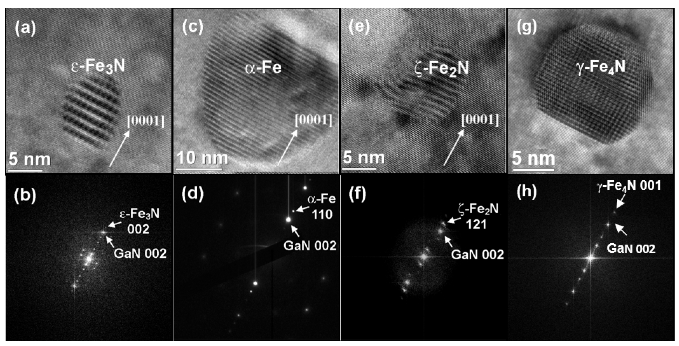
The aggregation of the magnetic ions during the growth of GaFeN in a MOVPE process is affected by growth rate and co-doping with shallow impurities [64]. While Si co-doping was found to hinder the aggregation of Fe ions in GaN and modify the charge state of the dilute Fe ions from Fe to Fe [65], Mg co-doping showed a behavior dependent on the growth mode employed [66]. There is a competition between Mg and Fe to occupy the Ga cation substitutional sites. This results in a reduced efficiency of the Fe ion incorporation in the homogeneously grown Mg co-doped layers, leading to a dilute and purely paramagnetic system, while in the Mg co-doping mode the aggregation of Fe is enhanced, inducing the formation of ferromagnetic and antiferromagnetic FeN () phases [66] presented in Figure 7.

Figure 7.
Embedded FeN nanocrystals with in MOVPE grown GaFeN imaged by HRTEM and the corresponding fast-Fourier transformation images: (a,b) -FeN, (c,d) -Fe, (e,f) -FeN, and (g,h) ’-FeN. Adapted from Reference [67].
Moreover, not only the employed growth-mode, but also the growth temperature (), modifies the stoichiometry of the embedded FeN nanocrystals in GaFeN and, therefore, their magnetic properties. The detailed characterization combining HRTEM, SXRD and SQUID magnetometry allowed the construction of a phase-diagram of the different FeN NCs as a function of the fabrication temperature for homogenously-doped GaFeN thin layers grown by MOVPE [67,68]. The magnetic properties of these layers depend entirely on the stoichiometry of the embedded FeN nanocrystals, displaying ferromagnetic and antiferromagnetic components [67,69]. X-ray magnetic circular dichroism (XMCD) measurements proved that the ferromagnetism in these layers is linked to the Fe(3d) states and that the N(2p) states carry considerable spin polarization, due to an exchange coupling with the Fe ions [70].
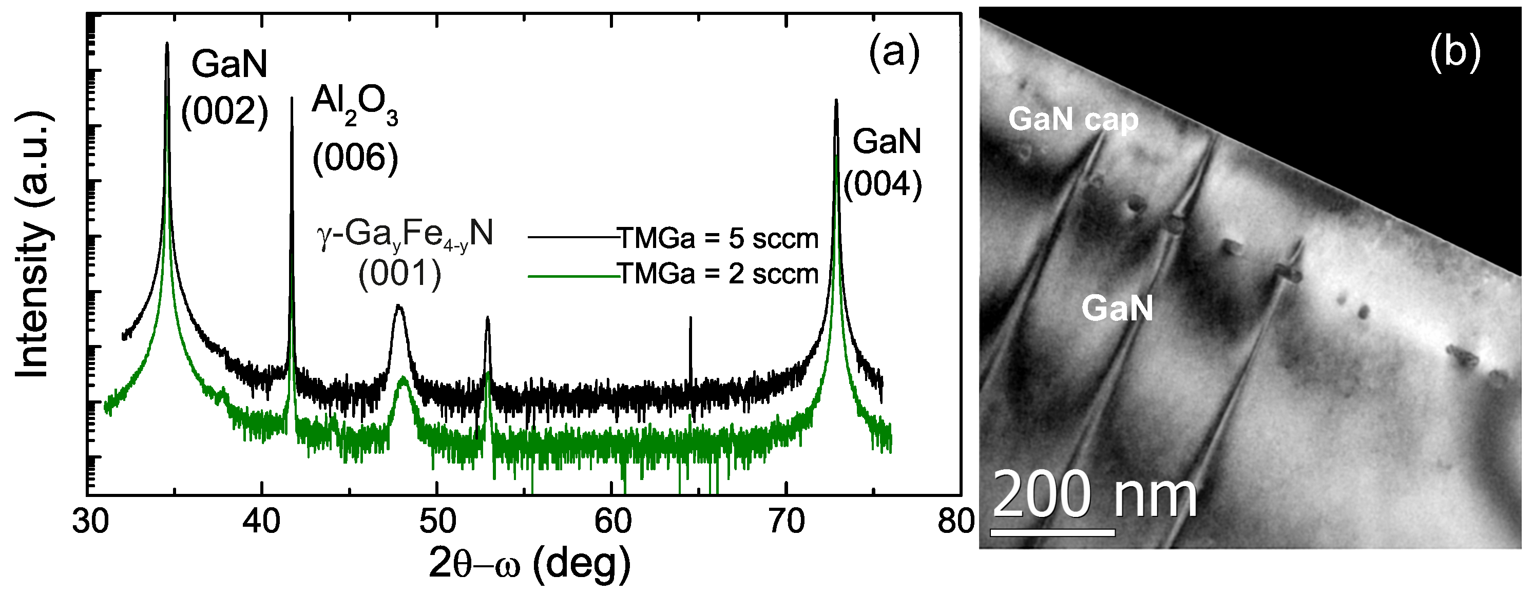
The employment of the -growth mode for the fabrication of GaFeN layers by MOVPE resulted in the formation of single-phase ’-GaFeN nanocrystal arrays localized in one plane close to the GaFeN/GaN interface [71,72,73], as presented in Figure 8. By varying the number of the employed -growth periods, the amount of Ga provided during the fabrication process can be adjusted. The resulting nanocrytsals are epitaxially embedded into the GaN matrix with an epitaxial relation (001)[110](0001)[1120] [71].

Figure 8.
Secondary phases in GaFeN layers identified from: (a) high-resolution XRD (HRXRD), and (b) cross-section TEM showing the planar ’-GaFeN nanocrystal arrays. Adapted from Reference [71].
While the phase, crystal structure and epitaxial relationship of the embedded nanocrystals are independent of the fabrication conditions, the size, shape and density are strongly fabrication dependent [73]. It was found that the amount of Ga supplied during the fabrication condition is the dominant parameter to achieve control over the size, shape and density of the nannocrystals. The Ga-flow provided during the -doping determines the amount of Fe incorporated, the spatial density of the NCs, as well as the aspect ratio of the NCs, and, consequently, the overall magnetic behavior of the system.
The magnetic properties of the -doped GaFeN layers are consistent with those of the homogenously Fe-doped GaN layers, displaying a superparamagnetic behavior with a ferromagnetic component persisiting above 390 K, associated to the oblate (20 ± 5) nm sized -GaFeN nanocrystals [69], and a uniaxial magnetic anisotropy with three in-plane easy axis [72]. Since the magnetic response of -GaFeN changes from strongly ferromagnetic () to weakly antiferromagnetic () [74,75], the planar arrays of -GaFeN nanocrystals embedded in GaN become suitable for ferromagnetic as well as for the emerging field of antiferromagnetic spintronics [76,77].
The overall conduction mechanism in these -doped GaFeN layers occurs at the unintentionally n-doped GaN buffer on which they are grown on. The behavior of the resistivity and the magnetoresistance (MR) in these layers can be described in terms of: (i) an Arrhenius-like mechanism for temperatures above 50 K and (ii) a variable range-hopping (VRH) conduction mechanism with inter-nanocrystal hopping conduction, where the spin polarized current is transported between nanocrystals at temperatures below 25 K [78]. Additionaly, the layers exhibit a positive out-of-plane anisotropic magnetoresistance of 16% at 2 K and 3% at 300 K attributed to the embedded nanocrystals, which is significantly larger than that previously reported for ’-FeN thin films [79].
When the -doped GaFeN layers were left uncapped, the formation of -Fe NCs located at the sample surface, was observed [78]. This is attributed to the evaporation of nitrogen taking place during the MOVPE process [80]. The presence of the -Fe nanocrystals showed an increased strong ferromagnetic contribution in the layers, while leaving the (magneto)transport properties unaffected [78].
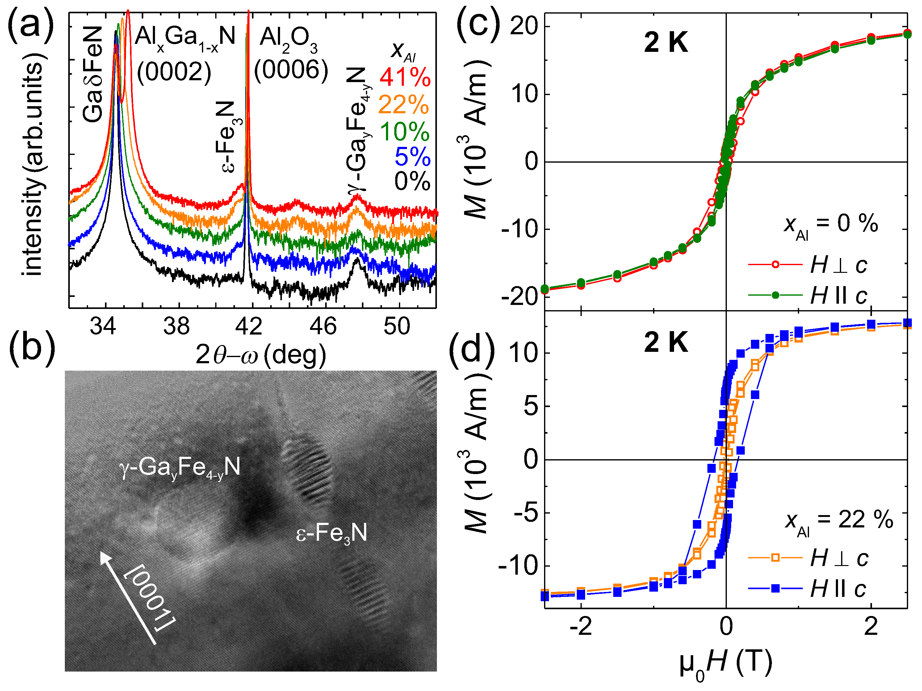
Interestingly, by adding Al into the buffer on which the -doped GaFeN layers were grown, the additional formation of elongated prolate -FeN nanocrystals is induced. This leads to a change in the magnetic easy axis from in-plane to out-of-plane and a sizeable out-of-plane magnetic anisotropy in the layers [81], displayed in Figure 9, opening the perspectives for an all-nitride based memory device.

Figure 9.
Shape-induced magnetic anisotropy in GaFeN/AlGaN heterostructures containing -FeN and ’-GaFeN as observed by (a) HRXRD and (b) HRTEM. Out-of-plane magnetic anisotropy of the layers grown on AlGaN buffers with (c) and (d) . Adapted from Reference [81].
3.3. Summary of the Secondary Phases Observed in GaFeN
The above results have shown that the most common observed secondary phase forming in GaFeN layers is the -FeN phase that is ferromagnetic with a above RT. However, depending on the employed growth conditions, the formation of numerous FeN phases with have been also reported. The main properties – structure and magnetism – of the secondary phases found in GaFeN layers are summarized in Table 2. The growth method and the growth mode employed is also specified: h stands for homogenous, and for the interrupted -growth mode.

Table 2.
Observed secondary- phases in GaFeN, their structural and magnetic properties, as well as the growth technique employed for the growth of the phase-separated layers.
4. Cr-Doped III-Nitrides
The doping of III-Nitrides with Cr atoms has been a subject of numerous publications where ferromagnetism with above RT has been reported [50,87,88,89,90,91,92]. The formation of secondary phases as the source for the observed ferromagnestim was often ruled out, while the origin was attributed to magnetic long-range interaction between the diluted Cr atoms. However, computational methods predicted on the one side the tendency of Cr ions to aggregate, favouring the formation of Cr nanoclusters with ferromagnetic interaction for clusters with two ions and antiferromagnetic interaction for clusters with more than two ions [93]. On the other side, short-ranged interactions between Cr ions and low in the GaCrN DMS were calculated [94], suggesting the origin for the observed high in the formation of ferromagnetic secondary phases and nanoclusters. Very few detailed nanocharacterization studies exist about for Cr-doped III-Nitride systems where the formation of secondary phases was identified [88,90,95].
4.1. Phase Separation in AlCrN Layers
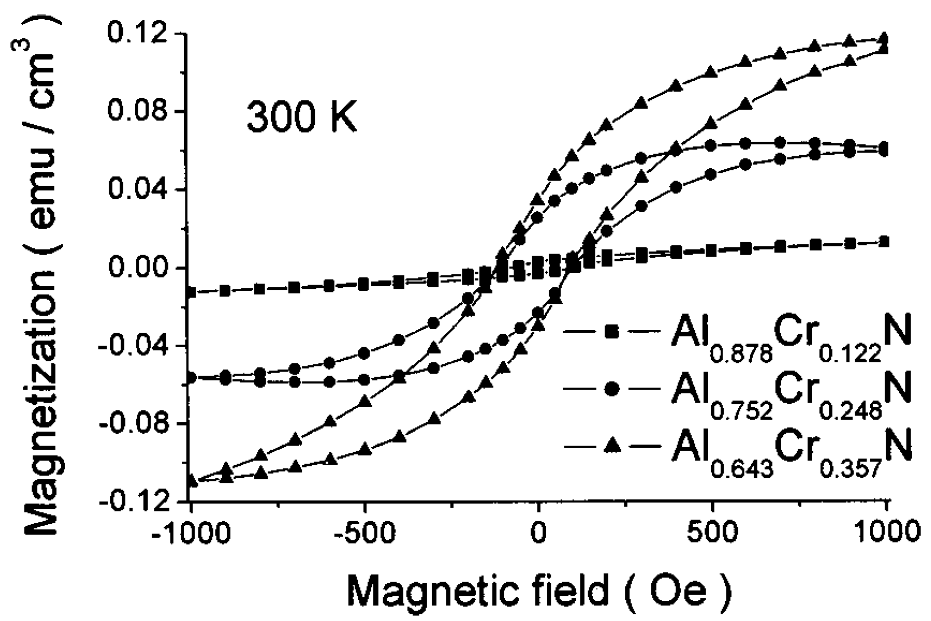
In Cr-doped AlN layers fabricated by reactive co-sputtering with Cr concentrations ranging between 12% to 36%, the formation of secondary phases could not entirely be ruled out based solely on XRD [87]. The magnetometry results, which revealed hysteresis with a coercivity independent of the Cr concentration in the layers as depicted in Figure 10, pointed at the existence of a ferromagnetic secondary CrN phase with fixed composition. However, the orgin of the ferromagnetic signatures was discussed in the frame of magnetic percolation and Cr-Cr magnetic interactions due to the high Cr atom concentrations in the layers. The AlCrN layers exhibited a decreasing resistivity with increasing Cr concentration and VRH type conduction properties.

Figure 10.
Magnetization of AlCrN layers prepared by reactive co-sputtering displaying room temperature (RT) ferromagnetism and fixed coercivity for the entire Cr concentration range 0.12–0.36, pointing at the formation of secondary phases. Reproduced with permission from Reference [87].
The dependence on the growth temperature in MBE grown AlCrN layers with 2% of Cr ions showed the formation of single-phase, resistive layers with ferromagnetic behaviour persisiting up to 350 K when grown below 1000 °C [88]. In the layers grown at temperatures above 1000 °C, secondary phases identified as CrN and AlCr (possibly AlCr and AlCr) were detected by Powder XRD. The phase-separated AlCrN layers were conductive, in contrast to the single-phase layers. Polyakov et al. [96] investigated the optical and electrical properties in detail of these AlCrN layers grown below and above 1000 °C. The increased resistivity in the single-phase layers is attributed to the deep-state of Cr formed in the band gap of AlN [97]. A reduction in the optical transmission observed in the AlCrN layers containing secondary phases, infers a shift of the band gap from 6.2 eV to 5.8 eV in the multi-phase material explained by the absorption through free carriers and strong scattering, due to the presence of conductive nanoclusters. These conductive nanoclusters are responsible for the large VRH-type conductive behavior of the layers.
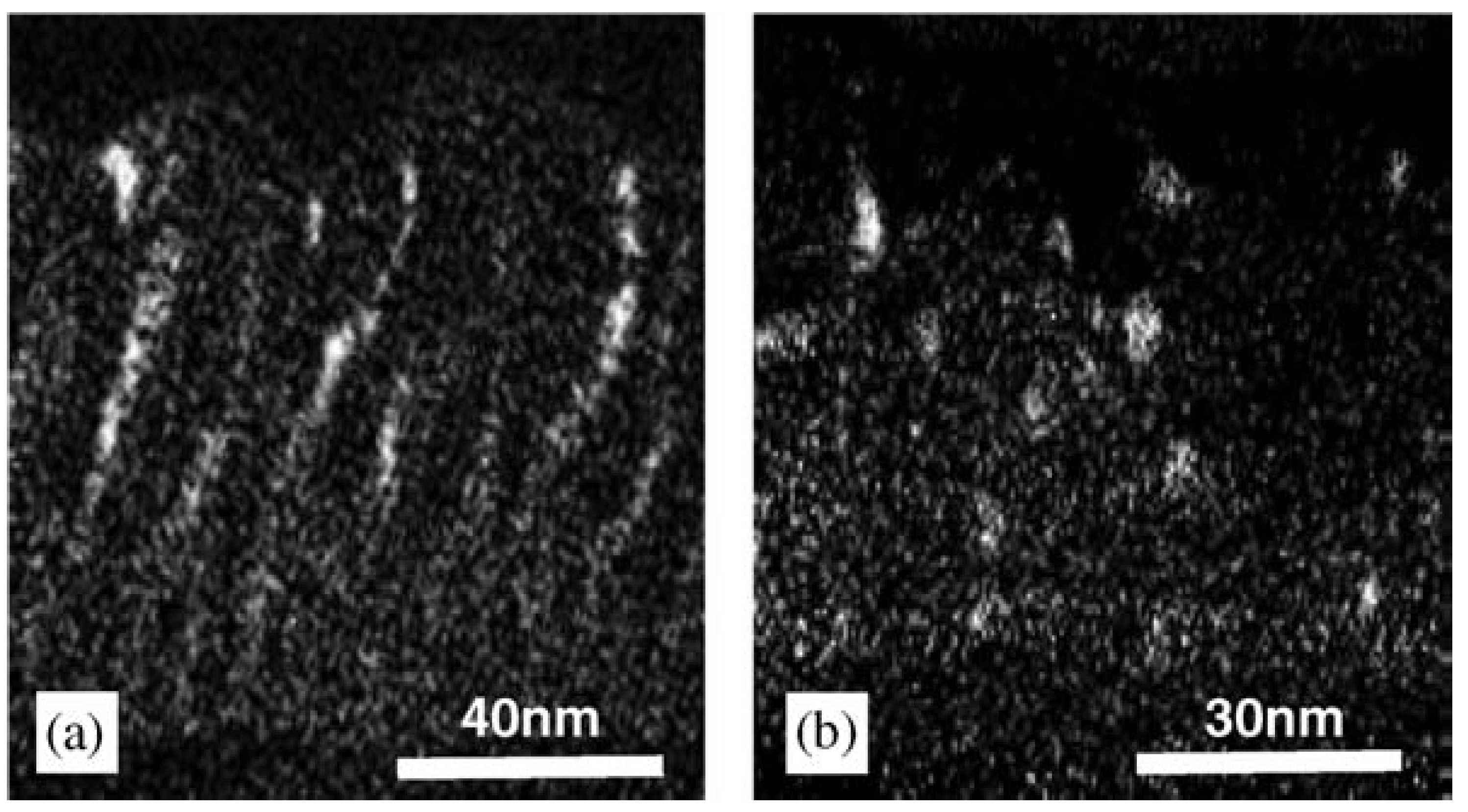
The nanocharacterization via HRTEM and energy filtered TEM, showed the formation of a microcolumnar morphology, where the Cr ions tend to cluster in AlCrN thin films grown by reactive MBE [90,97]. Already for , nanoclustering of the Cr into the columnar morphology was observed [90] if the layers were grown at 700 °C. If the layers were grown at 800 °C, the Cr formed spherical nanoclusters randomly distruibuted in the layer, as observed in Figure 11. These phase-separated layers are ferromagnetic with the highest and magnetization per Cr atom observed for the AlCrN layer of 900 K and 0.6, respectively. The orign of the observed ferromagnetism is left open, while the formation of CrN phases is completely excluded, based on the fact that most of the CrN phases are known to be antiferromagnetic, except for the CrN phase [98]. It is believed that the nanoaggregation of Cr into the columnar structure favours the Cr-Cr interaction in the layers or that the ferromagnetic interaction takes place due to the depletion of electrons from the Cr-Al level by compensating acceptors [97].

Figure 11.
Energy filtered TEM showing the Cr nanoaggregation into the columnar morphology in AlCrN with 4% Cr prepared at two fabrication temperatures: (a) 700 °C, and (b) 800 °C. Reproduced with permission from Reference [90].
4.2. Embedded CrN Nanostructures in GaN
Energy density calculations predicted that the Cr distribution in GaN is not random or homogeneous but that it is energetically favourable for the Cr atoms to form clusters. For clusters larger than two atoms an antiferromagnetic interaction will be energetically more favourable than the ferromagnetic one [93]. The cluster formation is enhanced both by increasing the Cr concentration and also by employing high growth temperatures during fabrication.
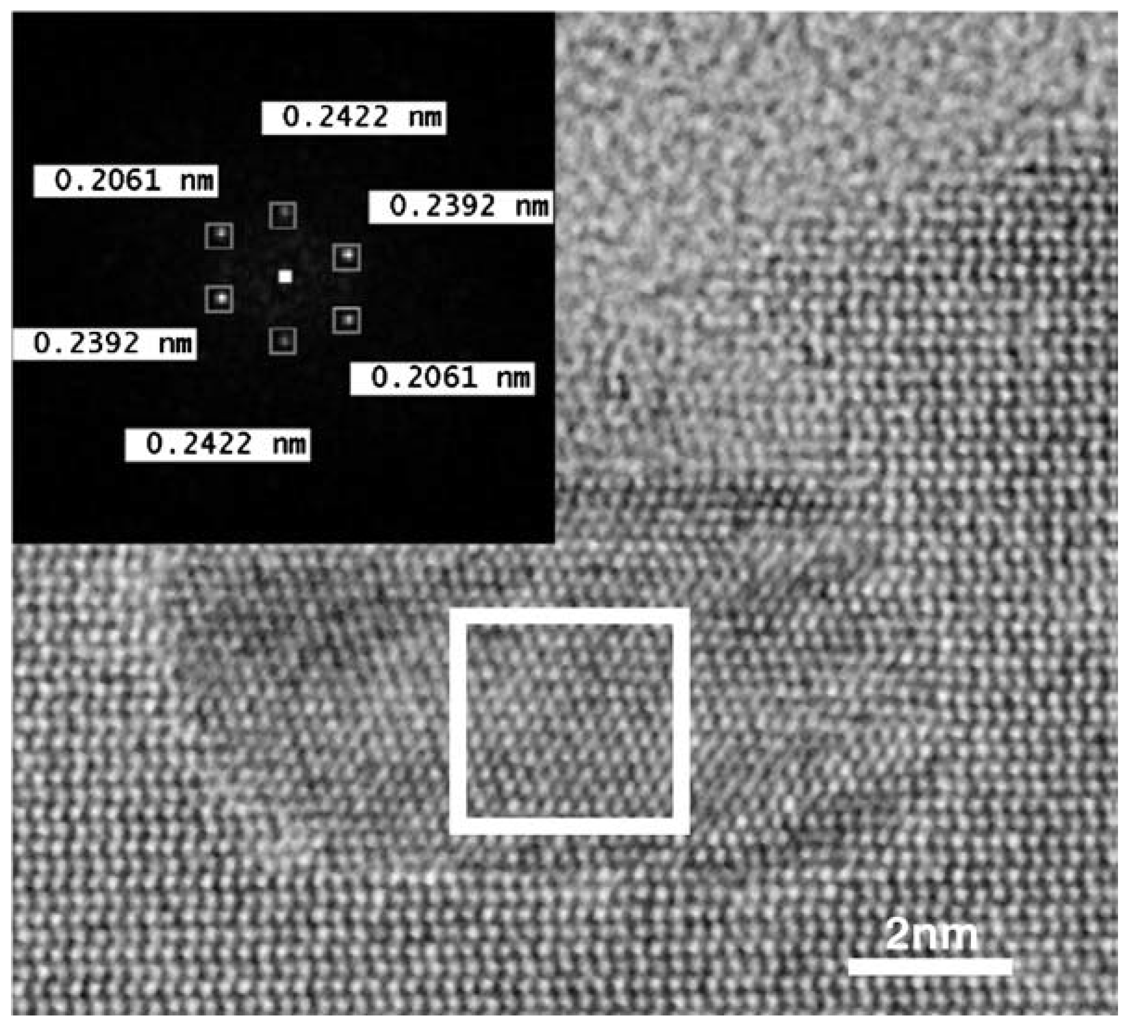
In reactive MBE grown GaCrN layers with 2% of Cr, the presence of small nanoclusters near to the surface were detected by HRTEM [90]. The nanoclusters were identified from the SADP as CrN having an epitaxial relation with the GaN matrix of (110)(0001), depicted in Figure 12. Rutherford back scattering measurements indicated that up to 70% of the Cr ions are located in substitutional sites, which is lower than that found for AlCrN layers grown with the same concentration, where 90% of the Cr is in substitutional sites [96]. The GaCrN layers show an even higher than the one reported for AlCrN layers of around 1000 K, which origin is left open [99]. The presence of the few CrN nanoclusters is not taken into consideration, as this phase is known to be antiferromagnetic [100].

Figure 12.
CrN nanocluster embedded in GaCrN probed by HRTEM and identified from the SADP shown in the inset. Reproduced with permission from Reference [90].
Magnetotransport measurements of the layers showed that the layers were highly conductive and presented a VRH-type conduction with a Coulomb gap. Furthermore, a negative MR of 3% at 2 K that decreases with increasing temperature was reported. While the conductive character of the layers was explained in the frame of the conduction electrons coming from the partially filled Cr levels, the presence of the CrN embedded nanoclusters conrtibuting to the conductive character like in the case of the phase-separated AlCrN [96] was not considered.
Silicon co-doping of GaCrN thin layers grown by electron-cyclotron-resonance MBE showed no phase separation from XRD and a ferromagnetic character persisiting to above 400 K [101]. Similar as in the cases of GaMnN and GaFeN, Si co-doping leads to a change in the charge state of Cr from Cr to Cr. Unexpectedly, a higher is observed for the Si co-doped layers, which is explained in terms of the formation of Cr-rich clusters due to the presence of Si. The authors emphasized the need for a detailed microscopic nanocharacterization of the Si do-doped GaCrN layers in order to fully understand their results.
An enhanced formation of CrN secondary phases is expected to occur through the addition of Mg to GaCrN layers [16], observed in the form of a low temperature splitting of the magnetic zero-field-cooled and field-cooled magnetometry curves. The observed splitting pointed at the formation of magnetic anisotropic nanoclusters below its blocking temperature () with a broad size distribution. According to DFT calculations, Cr atoms have the tendency to concentrate around N atoms and form CrN and CrN nanoclusters, which are both ferromagnetic [102].
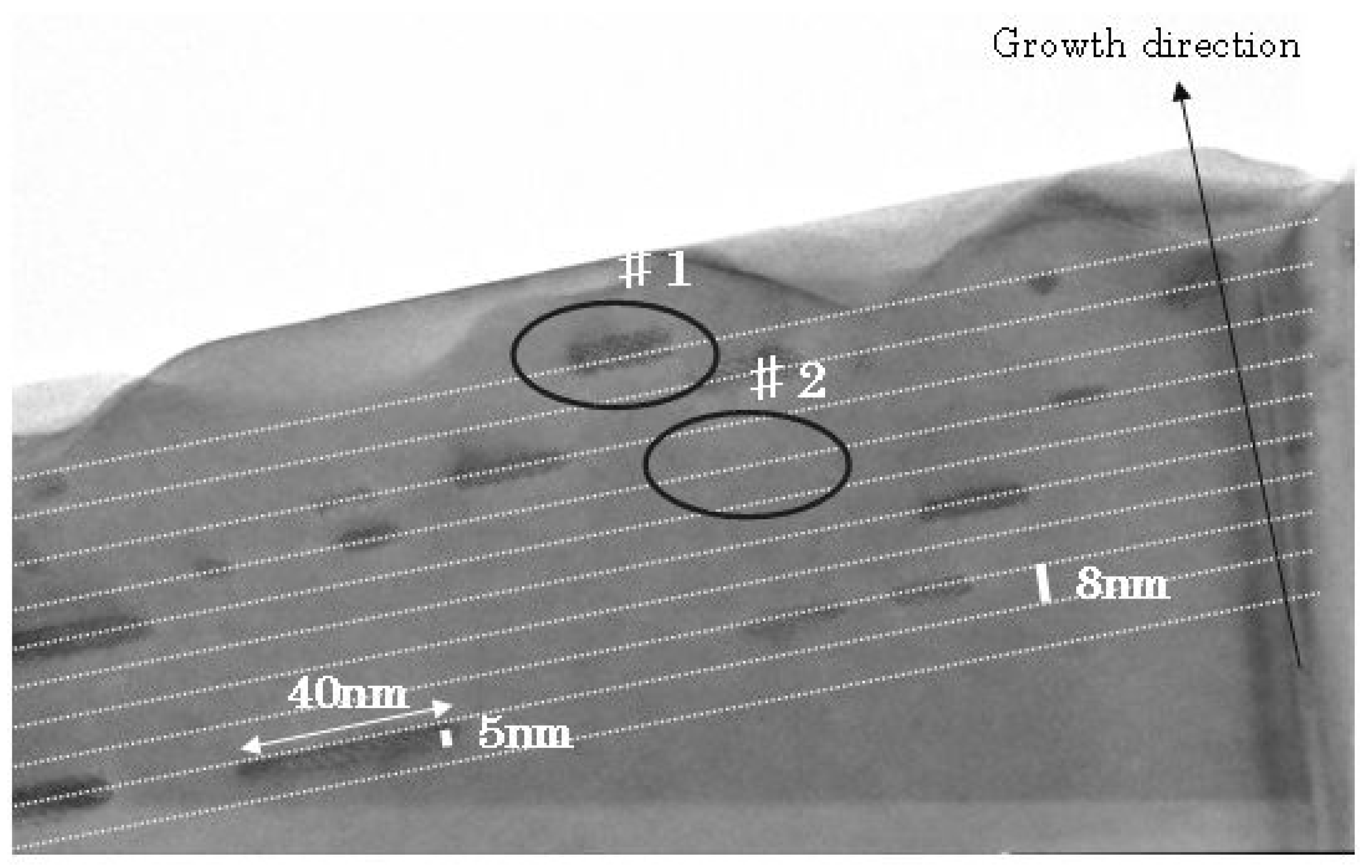
The -doping mode was also employed to grow aligned Cr-rich nanocluster arrays in GaCrN by radio-frequency MBE (RF-MBE) [95], motivated by the simulations of spinodal nanodecomposition by Katayama-Yoshida et al. where it was found that by controlling the decomposition dimensionality, various characteristic phases occur in DMSs: a threedimensional (3D) Dairiseki phase and a one-dimensional (1D) Konbu phase [94]. It was predicted that the superparamagnetic blocking temperature of GaCrN with a Konbu phase could be higher. The -doped layers consisted of Cr-periods grown between 8 nm GaN thin layers grown at different temperatures. By employing a growth temperature of 700 °C for the intermediate GaN layers, the formation of aligned CrN elongated nanostructures epitaxially embededd into the GaCrN surrounding matrix were found. The aligned nanoclusters, shown in Figure 13, had an epitaxial relation (0001) and [110] with the surrounding GaN matrix. Unfortunately, no details on the magnetic properties of the aligned CrN nanoclustersin GaCrN were provided.

Figure 13.
Aligned CrN nanoclusters in GaN grown by RF-MBE imaged by cross-section TEM. Reproduced with permission from Reference [95].
4.3. Summary of Secondary Phases Observed in III-Nitrides Doped with Cr
The nanoaggregation of Cr atoms into the columnar morphology in AlCrN was not considered as a phase separation, eventhough this type of Konbu phase was discussed in the frame of spinodal nanodecomposition occuring in DMS by Katayama-Yoshida et al. [94]. Additional phase separation was observed in both, Cr-doped AlN and GaN. The phases formed and observed in Cr-doped III-Nitrides layers are summarized in Table 3.

Table 3.
Observed secondary- phases in Cr-doped AlN and GaN, their structural and magnetic properties, as well as the growth technique of the layers.
5. Gd-Doped GaN
Investigations on RE doping of GaN started as an alternative for achieving tunable optoelctronic devices [17,98]. However, doping of GaN with RE, in particular with Gd, soon demonstrated their potential as suitable candidates for achieving high DMS [105,106,107,108,109,110].
The first observations of ferromagnetism GaGdN thin films grown by RF-MBE with 400 K were reported by Teraguchi et al. [105], where the presence of secondary phases such as Gd and GdN were ruled out due to their low reported of 308 K and 72 K, respectively [111]. Gd-doped GaN became a particularly interesting DMS after the observation of a colossal magnetic moment of 4000 per Gd ion in RF-MBE GaGdN layers with [106,112].
The origin of the observed colossal magnetic moment and the high in the DMS was then extensively discussed. It was consensly attributed to the existence of defects created during the incorporation of Gd ions into the GaN lattice, which amount depends largely on the growth mode employed [113]. These defects created through the Gd ions were expected to lead to a strain field around the Gd atoms in GaN and create therefore a potential dip around each Gd atom due to the large piezoelctric polarization of GaN, trapping carriers that could be spin polarized [107]. In particular, interstitial Ga, N, and O in octahedral sites next to the Gd ions were identified as the most probable sources of the observed ferromagnetism [110,114,115,116]. First-principle calculations attributed the colossal magnetic moment to the interaction of Gd 4f spins via p-d coupling involving holes introduced by intrinsic defects such as Ga vacancies [117,118].
Interestingly, like in the case of GaCrN, the magnetization of Si co-doped GaGdN layers increased with increasing Si co-doping reaching higher values that in the undoped material [119]. The same magnetization enhancement was observed for Mg co-doping [120]. In contrast, co-doping with hydrogen decreased the magnetic moment, indicating that the ferromagnetism in GaGdN was stabilized by electrons [109].
5.1. Structure and Magnetism of Secondary Phases in GaGdN
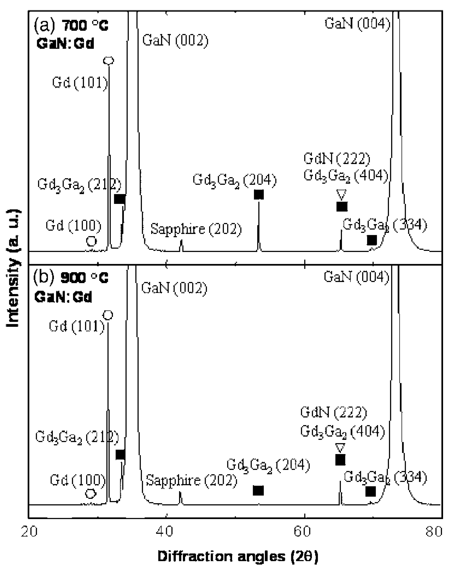
Similar as TM in III-Nitrides, Gd in GaN was found to substitute for the Ga cation sites in a tetrahedral coordination [121]. First indications of phase separation in GaGdN was observed by Han et al. in Gd-implanted GaN with a concentration of 0.1% [122]. They observed secondary phase separation independent of the employed implantation energy, which had not been detected previously [107,108]. The secondary phases were identified from HRXRD as Gd, GdN and GdGa, shown in Figure 14. The layers displayed a superparamagnetic behavior with above RT. Due to the fact that the magnetic properties of the observed GaGa phase were not known, the contribution of this phase to the overall magnetization could not be estimated. The other two phases, Gd and GdN, are known to be ferromagnetic, but because their is much lower than the one of the GaGdN layers, they were excluded as the origin of the observed ferromagnetism.

Figure 14.
Secondary phases identified by XRD in Gd-implanted GaN thin layers annealed at (a) 700 °C and (b) 900 °C. Reproduced with permission from Reference [122].
Onset of phase separation was also observed in plasma-assisted MBE grown GaGdN layers with a Gd concentration of 2.9% by employing a combination of circular and linear magnetic dichroism and ferromagnetic resonance [123]. It was found that the magnetic signatures of the sample corresponded to a superparamagnetic system containing Gd-clusters with a of 70 K, which is consistent with the literature values of the of GdN [124].
Interestingly, phase-separation was observed already for layers containing Gd ions in the concentration range between 0.0004–0.06% by employing a combination of detailed TEM techniques and geometric phase analysis simulations, shown in Figure 15 [125]. The formation of ultrathin, coherently strained GdN nanoplatelets lying parallel to the basal plane of the GaN matrix was observed. The density of the nanoplatelets increased with increasing Gd concentration in the layers, while the mean nanoplatelet size increased only from 2 nm to 4 nm from the lowest to the highest Gd concentrated sample. The implications of these GdN nanoplatelets on the magnetic properties of the layers was not discussed. However, these results underlined the importance of a detailed nanocharacterization in magnetic semiconductors treated as diluted, but where spinodal nanodecomposition has taken place [11].
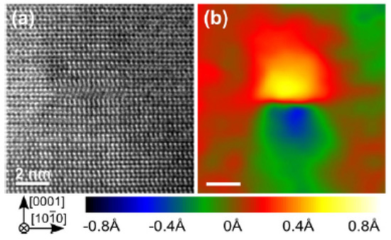
Figure 15.
Identified GdN nanoplatelet in GaGdN from: (a) HRTEM and (b) displacement-field mapping along the [0001] direction. Reproduced with permission from Reference [125].
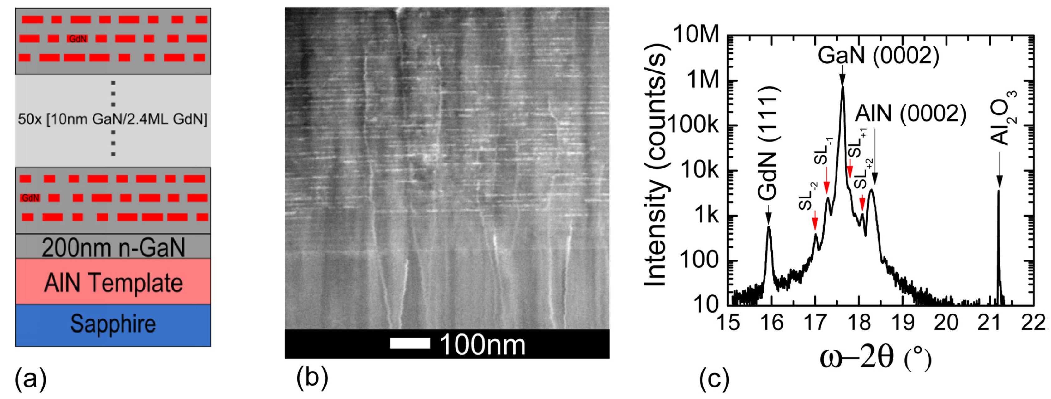
Through the implementation of a -doping-like growth mode in MBE grown GdN/GaN superlattices deposited onto GaN/AlO MOVPE templates, the formation of GdN nanoislands was observed [126]. The superlattices consisted of ultrathin layers of GdN (0.2 ML) separated by 10 nm thick GaN spacer layers, resulting in the formation of GdN elongated cubic nanoislands embedded in the hexagonal GaN matrix after the deposition of 1.2 ML of GdN (6 periods), presented in Figure 16. The size of the nanoislands along the growth direction was constant, while the increase in the Gd supplied during the growth increased only their lateral size, similar as the behaviour observed of ’-GaFeN embedded nanocrystals found in -doped GaFeN layers [73]. The epitaxial relation of the GdN nanoislands along the growth direction was found to be (111)(0001).

Figure 16.
GdN nanoislands embedded in a GaN/GdN superlattice. (a) Sample structure, (b) cross-section high angle annular dark-field scanning TEM of the superlattice structure, and (c) HRXRD showing the orientation of the GdN embedded nanoislands in the GaN matrix. Reproduced with permission from Reference [126].
The magnetic characteristics of the GaGdN superlattice containing GdN nanoislands consisted of two contributions: (i) a dominating, isotropic magnetic component from the GdN nanoislands with K, and (ii) a weak, anisotropic ferromagnetic component that persists up to above RT, which is attributed to the interaction of Gd with the lattice defects in the GaN matrix, consistently with previous results on singe-phase GaGdN [106]. At temperatures below 70 K, an additional paramagnetic component attributed to the substitutional Gd ions in GaN was also observed. The weak ferromagnetic component, attributed to the defects, displayed out-of-plane magnetic anisotropy.
It has been demonstrated that these epitaxially embedded GdN nanoislands in GaN can be employed for efficient interband tunnelling in GaN junctions [127]. An efficient tunnel injection of holes from a n-type GaN top contact into the p-type GaN was achieved, demonstrating a low tunnel junction specific contact resistivity of 1.3 ×–cm. This demonstration of efficient tunnelling using GdN nanoislands opens the perspectives for designing III-nitride electronic and optoelectronic devices with higher performance and functionality.
5.2. Summary of Secondary Phases Observed in GaGd
The high observed in GaGdN layers has been attributed to the presence of defects: Ga, N and O vacancies and interstitials. In this material system, the formation and presence of secondary phases is not necessary linked to the magnetic properties. Nevertheless, it has been shown that phase decomposition occurs already for concentrations of Gd in the order of ions/cm. The reported secondary phases in GaGdN are listed in Table 4.

Table 4.
Observed secondary- phases in Gd-doped GaN, their structural and magnetic properties, as well as the growth technique of the phase-separated layers.
6. Summary and Outlook
The formation of secondary phases in III-Nitride-based magnetic semiconductors and their role on the observed magnetic properties have been reviewed. It has been shown, that the low solubility limit of TM and RE magnetic ions in III-Nitrides, lying often in a few percent of magnetic ions, should not be regarded as a drawback, but as an advantage that open numerous perspectives for these phase-separated materials.
The incorporation of both, TM and RE ions, usually occurs substituting for the III-cations in a 3+ charge state, which is usually changed to a 2+ charge state through co-doping with Si. The magnetic properties of these phase-separated III-Nitrides consist of at least two contributions: (i) a paramagnetic contribution attributed to the dilute substitutional 3+ magnetic ions in the III-Nitride matrix, and (ii) a magnetic component dominant at RT associated to the secondary phases, which can be either ferromagnetic, antiferromagnetic or superparamagnetic.
The often controversial origin of high ferromagnetism in many III-Nitride-based magnetic semiconductors has in the case of TM-doped GaN, been identified as originating from the formation of ferromagnetic secondary phases epitaxially embedded in the hexagonal matrix. While in Gd-doped GaN the colossal magnetic moment and high ferromagnetism is attributed to formation of defects formed during the incorporation of the magnetic dopant.
The above presented results underline the importance of a detailed nanocharacterization through the combination of high-resolution spectroscopic, imaging and computational techniques in order to gain full insight into the nanostructure and the origin of the observed magnetic features in III-Nitride magnetic semiconductors, which also applies to numerous other material systems [11].
The embedded nanostructures and their properties, like phase, size and density, can be often tuned on demand by adjusting the fabrication conditions and depend largely on the growth mode and growth technique employed. The fabrication of self-assembled nanostructured arrays in Fe, Cr and Gd-doped GaN by employing an interrupted -growth mode has been achieved, opening wide perspectives for their implementation into functional devices. The observation of out-of-plane magnetic anisotropy in -GaFeN/AlGaN heterostructures and GdN/GaN superlattices and the manipulation of the aligned nanostructures through magnetic and electric fields, makes them appealing for their implementation into memory device-like structures.
This review demonstrates the large potential of III-Nitride CMS, where still many challenging physics are yet expected to be discovered when investigating proximity effects in combination with 2D van der Waals structures, superconductors and topological insulators [128,129].
Funding
The current work has been funded by the Austrian Science Fund FWF Project No. V478-N36.
Acknowledgments
The author greatly acknowldeges the funding by the Austrian Science Fund FWF through the Elise Richter project V478-N36. Open Access Funding by the Austrian Science Fund (FWF).
Conflicts of Interest
The author declares no conflict of interest.
References
- Binasch, G.; Gruenberg, P.; Saurenbach, F.; Zinn, W. Enhanced magnetoresistance in layered magnetic structures with antiferromagnetic interlayer exchange. Phys. Rev. B 1989, 39, 4828. [Google Scholar] [CrossRef] [PubMed]
- Baibich, M.N.; Broto, J.M.; Fert, A.; Dau, F.N.V.; Petroff, F.; Etienne, P.; Creuzet, G.; Friedrich, A.; Chazelas, J. Giant Magnetoresistance of (001)Fe/(001)Cr Magnetic Superlattices. Phys. Rev. Lett. 1988, 61, 2472. [Google Scholar] [CrossRef] [PubMed]
- Furdyna, J.K.; Kossut, J. Diluted Magnetic Semiconductors; Academic Press: New York, NY, USA, 1988. [Google Scholar]
- Dietl, T. Diluted Magnetic Semiconductors; North-Holland: New York, NY, USA, 1994. [Google Scholar]
- Ohno, H. Making Nonmagnetic Semiconductors Ferromagnetic. Science 1998, 281, 951. [Google Scholar] [CrossRef]
- Chiba, D.; Sawicki, M.; Nishitani, Y.; Nakatani, Y.; Matsukura, F.; Ohno, H. Magnetization vector manipulation by electric fields. Nature 2008, 455, 515. [Google Scholar] [CrossRef] [PubMed]
- Chen, L.; Yang, X.; Yang, H.F.; Zhao, J.; Misuraca, J.; Xiong, P.; Von Molnár, S. Enhancing the Curie Temperature of Ferromagnetic Semiconductor (Ga,Mn)As to 200 K via Nanostructure Engineering. Nano Lett. 2011, 11, 2584–2589. [Google Scholar] [CrossRef]
- Dietl, T.; Ohno, H.; Matsukura, F.; Cibert, J.; Ferrand, D. Zener Model Description of Ferromagnetism in Zinc-Blende Magnetic Semiconductors. Science 2000, 287, 1019. [Google Scholar] [CrossRef]
- Bonanni, A.; Dietl, T. A story of high-temperature ferromagnetism in semiconductors. Chem. Soc. Rev. 2010, 39, 528. [Google Scholar] [CrossRef]
- Dietl, T. A ten-year perspective on dilute magnetic semiconductors and oxides. Nat. Mater. 2010, 9, 965–974. [Google Scholar] [CrossRef]
- Dietl, T.; Sato, K.; Fukushima, T.; Bonanni, A.; Jamet, M.; Barski, A.; Kuroda, S.; Tanaka, M.; Hai, P.N.; Katayama-Yoshida, H. Spinodal nanodecomposition in semiconductors doped with transition metals. Rev. Mod. Phys. 2010, 87, 1311. [Google Scholar] [CrossRef]
- Coey, J.; Smith, P. Magnetic nitrides. J. Magn. Magn. Mater. 1999, 200, 405–424. [Google Scholar] [CrossRef]
- Chen, L.; Matsukura, F.; Ohno, H. Direct-current voltages in (Ga,Mn)As structures induced by ferromagnetic resonance. Nat. Commun. 2013, 4, 2055. [Google Scholar] [CrossRef] [PubMed]
- Jensen, P.J.; Pastor, G.M. Low-energy properties of two-dimensional magnetic nanostructures: Interparticle interactions and disorder effects. New J. Phys. 2003, 5, 1–22. [Google Scholar] [CrossRef]
- Bonanni, A. Ferromagnetic nitride-based semiconductors doped with transition metals and rare-earths. Semicond. Sci. Technol. 2007, 22, R41. [Google Scholar] [CrossRef]
- Kane, M.H.; Gupta, D.; Ferguson, I.T. Transition Metal and Rare Earth Doping in GaN; Woodhead Publishing: Cambridge, UK, 2016; pp. 315–370. [Google Scholar]
- Zavada, J.M. Magnetic III-N Semiconductors Based on Rare Earth Doping. ECS Trans. 2019, 89, 17. [Google Scholar] [CrossRef]
- Santos, J.P.T.; Marques, M.; Teles, L.K.; Ferreira, L.G. Antiferromagnetism with spin polarization of GaN-based diluted magnetic semiconductors. Phys. Rev. B 2010, 81, 115209. [Google Scholar] [CrossRef]
- Gonzalez-Swacki, N.; Majewski, J.A.; Dietl, T. Aggregation and magnetism of Cr, Mn, and Fe cations in GaN. Phys. Rev. B 2011, 83, 184417. [Google Scholar] [CrossRef]
- Dhar, S.; Brandt, O.; Trampert, A.; Friedland, K.J.; Sun, Y.J.; Ploog, K.H. Observation of spin-glass behavior in homogeneous (Ga,Mn)N layers grown by reactive molecular-beam epitaxy. Phys. Rev. B 2003, 67, 165205. [Google Scholar] [CrossRef]
- Sonoda, S.; Shimizu, S.; Sasaki, T.; Yamamoto, Y.; Horia, H. Molecular beam epitaxy of wurtzite (Ga,Mn)N films on sapphire(0 0 0 1) showing the ferromagnetic behaviour at room temperature. J. Cryst. Growth 2002, 237–239, 1358. [Google Scholar] [CrossRef]
- Sawicki, M.; Devillers, T.; Gałeski, S.; Simserides, C.; Dobkowska, S.; Faina, B.; Grois, A.; Navarro-Quezada, A.; Trohidou, K.N.; Majewski, J.A.; et al. Origin of low-temperature magnetic ordering in Ga1−xMnxN. Phys. Rev. B 2012, 85, 205204. [Google Scholar] [CrossRef]
- Kunert, G.; Dobkowska, S.; Li, T.; Reuther, H.; Kruse, C.; Figge, S.; Jakieła, R.; Bonanni, A.; Grenzer, J.; Stefanowicz, W.; et al. Ga1−xMnxN epitaxial films with high magnetization. Appl. Phys. Lett. 2012, 101, 022413. [Google Scholar] [CrossRef]
- Stefanowicz, S.; Kunert, G.; Simserides, C.; Majewski, J.A.; Stefanowicz, W.; Krusse, C.; Figge, S.; Li, T.; Jakieła, R.; Trohidou, K.; et al. Phase diagram and critical behavior of the random ferromagnet Ga1−xMnxN. Phys. Rev. B 2013, 88, 081201(R). [Google Scholar] [CrossRef]
- Zaja̧c, M.; Doradziński, R.; Gosk, J.; Sczytko, J.; Lefeld-Sosnowska, M.; Kamińska, M.; Twardowski, A.; Palczweska, M.; Grzanka, E.; Gȩbicki, W. Magnetic and optical properties of GaMnN magnetic semiconductor. Appl. Phys. Lett. 2001, 78, 9. [Google Scholar] [CrossRef]
- Granville, S.; Ruck, B.J.; Budde, F.; Trodhal, H.J.; Williams, G.V.M. Nearest-neighbor Mn antiferromagnetic exchange in Ga1−xMnxN. Phys. Rev. B. 2010, 81, 184425. [Google Scholar] [CrossRef]
- Sedmidubský, D.; Leitner, J.; Soferr, Z. Phase relations in the Ga-Mn-N system. J. Alloys Compd. 2008, 452, 105–109. [Google Scholar] [CrossRef]
- Leineweber, A.; Niewa, R.; Jacobs, H.; Kockelmann, W. The manganese nitrides Mn3N2 and Mn6N5−x: Nuclear and magnetic structures. J. Mater. Chem. 2000, 10, 2827. [Google Scholar] [CrossRef]
- Zaja̧c, M.; Gosk, J.; Grzanka, E.; Kamińska, M.; Twardowski, A.; Strojek, B.; Szyszko, T.; Podsiadło, S. Possible origin of ferromagnetism in (Ga,Mn)N. J. Appl. Phys. 2003, 93, 4715–4717. [Google Scholar] [CrossRef]
- Suzuki, K.; Kaneko, T.; Yoshida, H.; Obi, Y.; Fujimori, H.; Morita, H. Crystal structure and magnetic properties of the compound MnN. J. Alloys Compd. 2000, 306, 66–71. [Google Scholar] [CrossRef]
- Li, C.; Yang, Y.; Lv, L.; Huang, H.; Wang, Z.; Yang, S. Fabrication and magnetic characteristic of ferrimagnetic bulk Mn4N. J. Alloys Compd. 2008, 457, 57–60. [Google Scholar] [CrossRef]
- Baik, J.M.; Kim, H.S.; Park, C.G.; Lee, J.L. Effect of microstructural evolution on magnetic property of Mn-implanted p-type GaN. Appl. Phys. Lett. 2003, 83, 13. [Google Scholar] [CrossRef]
- Niida, H.; Hori, T.; Nakagawa, Y. Magnetic Properties and Crystal Distortion of Hexagonal Mn3Ga. J. Phys. Soc. Jpn. 1983, 52, 1512–1514. [Google Scholar] [CrossRef]
- Balke, B.; Fecher, G.H.; Winterlik, J.; Felser, C. Mn3Ga, a compensated ferrimagnet with high Curie temperature and low magnetic moment for spin torque transfer applications. App. Phys. Lett. 2007, 90, 152504. [Google Scholar] [CrossRef]
- Eddine, M.N.; Bertaut, E. Structure cristallographic et magnetique de Mn2N0.86. Solid State Commun. 1977, 23, 147–150. [Google Scholar] [CrossRef]
- Sun, L.; Yan, F.; Gao, H.; Zhang, H.; Zeng, Y.; Wang, G.; Li, J. Structure and magnetic characteristics of nonpolar a-plane GaN:Mn films. J. Phys. D Appl. Phys. 2008, 41, 165004. [Google Scholar] [CrossRef]
- Sztenkiel, D.; Foltyn, M.; Mazur, G.; Adhikari, R.; Kosiel, K.; Gas, K.; Zgirski, M.; Kruszka, R.; Jakieła, R.; Li, T.; et al. Stretching magnetism with an electric field in a nitride semiconductor. Nat. Commun. 2016, 7, 13232. [Google Scholar] [CrossRef]
- Kim, K.H.; Lee, K.J.; Kim, D.J.; Kim, H.J.; Ihm, Y.E.; Djayaprawira, D.; Takahashi, M.; Kim, C.S.; Kim, C.G.; Yoo, S.H. Magnetotransport of p-type GaMnN assisted by highly conductive precipitates. Appl. Phys. Lett. 2003, 82, 1775. [Google Scholar] [CrossRef]
- Kuroda, S.; Bellet-Amalric, E.; Giraud, R.; Marcet, S.; Cibert, J.; Mariette, H. Strong influence of Ga/N flux ratio on Mn incorporation into Ga1−xMnx epilayers grown by plasma-assisted molecular beam epitaxy. Appl. Phys. Lett. 2003, 83, 4580–4582. [Google Scholar] [CrossRef]
- Giraud, R.; Kuroda, S.; Marcet, S.; Bellet-Amalric, E.; Biquard, X.; Barbara, B.; Fruchart, D.; Ferrand, D.; Cibert, J.; Mariette, H. Ferromagnetic Ga1−xMnxN epilayers vs. antiferromagnetic GaMn3N clusters. Europhys. Lett. 2004, 65, 553–559. [Google Scholar] [CrossRef]
- Kocan, M.; Malindretos, J.; Roever, M.; Zenneck, J.; Niermann, T.; Mai, D.; Bertelli, M.; Seibt, M.; Rizzi, A. Mn incorporation in GaN thin layers grown by molecular-beam epitaxy. Semicond. Sci. Technol. 2006, 21, 1348–1353. [Google Scholar] [CrossRef]
- Miao, M.S.; Herwadkar, A.; Lambrecht, W.R.L. Electronic structure and magnetic properties of Mn3GaN precipitates in Ga1−xMnxN. Phys. Rev. B 2005, 72, 033204. [Google Scholar] [CrossRef]
- Song, B.; Jian, J.; Bao, H.; Lei, M.; Li, H.; Wang, G.; Xu, Y.; Chen, X. Observation of spin-glass behavior in antiperovskite Mn3GaN. Appl. Phys. Lett. 2008, 92, 192511. [Google Scholar] [CrossRef]
- Iye, Y.; Oiwa, A.; Ando, A.; Katsumoto, S.; Matsukura, F.; Shen, A.; Ohno, H.; Munekata, H. Metal–insulator transition and magnetotransport in III–V compound diluted magnetic semiconductors. Mater. Sci. Eng. B 1999, 63, 88. [Google Scholar] [CrossRef]
- Devillers, T.; Rovezzi, M.; Szwacki, N.G.; Dobkowska, S.; Stefanowicz, W.; Sztenkiel, D.; Grois, A.; Suffczynski, J.; Navarro-Quezada, A.; Faina, B.; et al. Manipulating Mn–Mgk cation complexes to control the charge- and spin-state of Mn in GaN. Sci. Rep. 2012, 2, 722. [Google Scholar] [CrossRef] [PubMed]
- Devillers, T.; Leite, D.M.G.; Da Silva, J.H.D.; Bonanni, A. Functional Mn–Mgk cation complexes in GaN featured by Raman spectroscopy. App. Phys. Lett. 2013, 103, 211909. [Google Scholar] [CrossRef]
- Kysylychyn, D.; Suffczynski, J.; Wozniak, T.; Szwacki, N.; Bonanni, A. Resonant excitation of infrared emission in GaN:(Mn,Mg). Phys. Rev. B 2018, 97, 245311. [Google Scholar] [CrossRef]
- Stefanowicz, W.; Sztenkiel, D.; Faina, B.; Grois, A.; Rovezzi, M.; Devillers, T.; Navarro-Quezada, A.; Li, T.; Jakieła, R.; Sawicki, M.; et al. Magnetism of dilute (Ga,Mn)N. Phys. Rev. B 2010, 81, 235210. [Google Scholar] [CrossRef]
- Capuzzo, G.; Kysylychyn, D.; Adhikari, R.; Li, T.; Faina, B.; Martín-Luengo, A.T.; Bonanni, A. All-nitride AlxGa1−xN:Mn/GaN distributed Bragg reflectors for the near-infrared. Sci. Rep. 2017, 7, 42697. [Google Scholar] [CrossRef]
- Ney, A.; Rajaram, R.; Arenholz, E.; Harris, J.S., Jr.; Samant, M.; Farrow, R.F.C.; Parkin, S.S.P. Structural and magnetic properties of Cr and Mn doped InN. J. Magn. Magn. Mater. 2006, 300, 7–11. [Google Scholar] [CrossRef]
- Heikmann, S.; Keller, S.; DenBaars, S.P.; Mishra, U.K. High temperature (>400 K) ferromagnetism in III-V-based diluted magnetic semiconductor GaCrN grown by ECR molecular-beam epitaxy. Appl. Phys. Lett. 2002, 81, 439. [Google Scholar]
- Bougrioua, Z.; Azize, M.; Jimenez, A.; Brania, A.F.; Lorenzini, P.; Beaumont, B.; Munioz, E.; Gibart, P. Fe doping for making resistive GaN layers with low dislocation density; consequence on HEMTs. Phys. Stat. Solidi C 2005, 2, 2424–2428. [Google Scholar] [CrossRef]
- Polyakov, A.Y.; Smirnov, N.B.; Govorkov, A.V.; Pearton, S.J. Electrical and optical properties of Fe-doped semi-insulating GaN templates. Appl. Phys. Lett. 2003, 83, 3314. [Google Scholar] [CrossRef]
- Ishiguro, T.; Yamada, A.; Kotani, J.; Nakamura, N.; Kikkawa, T.; Watanabe, K.; Imanishi, K. New Model of Fe Diffusion in Highly Resistive Fe-Doped Buffer Layer for GaN High-Electron-Mobility Transistor. Jpn. J. App. Phys. 2013, 52, 08JB17. [Google Scholar] [CrossRef]
- Heikmann, S.; Keller, S.; Mates, T.; DenBaars, S.P.; Mishra, U.K. Growth and characteristics of Fe doped GaN. J. Cryst. Growth 2003, 248, 513–517. [Google Scholar] [CrossRef]
- Therodoropoulou, N.; Hebard, A.F.; Chu, S.N.G.; Overgberg, M.E.; Abernathy, C.R.; Pearton, S.J.; Wilson, R.G.; Zavada, J.M. Characterization of high dose Fe implantation into p-GaN. Appl. Phys. Lett. 2001, 79, 3452–3453. [Google Scholar] [CrossRef]
- Schon, Y.; Kwon, Y.H.; Park, Y.S.; Yuldashev, S.U.; Lee, S.J.; Park, C.S.; Chung, J.; Yoon, S.J.; Kim, H.J.; Lee, W.C.; et al. The study of structural, optical, and magnetic properties of undoped and p-type GaN implanted with Mn+ (10 at.%). J. Appl. Phys. 2004, 95, 761–763. [Google Scholar]
- Talut, G.; Reuther, H.; Mücklich, A.; Eichhorn, F.; Potzger, K. Nanocluster formation in Fe implanted GaN. Appl. Phys. Lett. 2006, 89, 161909. [Google Scholar] [CrossRef]
- Talut, G.; Grenzer, J.; Reuther, H.; Shalimov, A.; Baehtz, C.; Novikov, D.; Walz, B. In situ observation of secondary phase formation in Fe implanted GaN annealed in low pressure N2 atmosphere. Appl. Phys. Lett. 2009, 95, 232506. [Google Scholar] [CrossRef]
- Talut, G.; Reuther, H.; Grenzer, J.; Mücklich, A.; Shalimov, A.; Skorupa, W.; Stromberg, F. Spinodal decomposition and secondary phase formation in Fe-oversaturated GaN. Phys. Rev. B 2010, 81, 155212. [Google Scholar] [CrossRef]
- Sato, K.; Katayama-Yoshida, H.; Dederichs, P.H. High Curie temperature and nano-scale spinodal decomposition phase in diluted magnetic semiconductors. Jpn. J. Appl. Phys. 2005, 44, L948–L951. [Google Scholar] [CrossRef]
- Bonanni, A.; Kiecana, M.; Simbrunner, C.; Li, T.; Sawicki, M.; Wegscheider, M.; Quast, M.; Przybylinska, H.; Navarro-Quezada, A.; Jakieła, R.; et al. Paramagnetic GaN:Fe and ferromagnetic (Ga,Fe)N: The relationship between structural, electronic, and magnetic properties. Phys. Rev. B 2007, 75, 125210. [Google Scholar] [CrossRef]
- Pacuski, W.; Kossacki, P.; Ferrand, D.; Golnik, A.; Cibert, J.; Wegscheider, M.; Navarro-Quezada, A.; Bonanni, A.; Kiecana, M.; Sawicki, M.; et al. Observation of Strong-Coupling Effects in a Diluted Magnetic Semiconductor Ga1−xFexN. Phys. Rev. Lett. 2008, 100, 037204. [Google Scholar] [CrossRef]
- Bonanni, A.; Navarro-Quezada, A.; Li, T.; Wegscheider, M.; Matěj, Z.; Holý, V.; Lechner, R.T.; Bauer, G.; Rovezzi, M.; D’Acapito, F.; et al. Controlled Aggregation of Magnetic Ions in a Semiconductor: An Experimental Demonstration. Phys. Rev. Lett. 2008, 101, 135502. [Google Scholar] [CrossRef] [PubMed]
- Rovezzi, M.; D’Acapito, F.; Navarro-Quezada, A.; Faina, B.; Li, T.; Bonanni, A.; Filippone, F.; Bonapasta, A.; Dietl, T. Local structure of (Ga,Fe)N and (Ga,Fe)N:Si investigated by x-ray absorption fine structure spectroscopy. Phys. Rev. B 2009, 79, 195209. [Google Scholar] [CrossRef]
- Navarro-Quezada, A.; GonzalezSzwacki, N.; Stefanowicz, W.; Li, T.; Grois, A.; Devillers, T.; Rovezzi, M.; Jakieła, R.; Faina, B.; Majewski, J.A.; et al. Fe-Mg interplay and the effect of deposition mode in (Ga,Fe)N doped with Mg. Phys. Rev. B 2011, 84, 155321. [Google Scholar] [CrossRef]
- Navarro-Quezada, A.; Stefanowicz, W.; Li, T.; Faina, B.; Rovezzi, M.; Lechner, R.T.; Devillers, T.; D’Acapito, F.; Bauer, G.; Sawicki, M.; et al. Embedded magnetic phases in (Ga,Fe)N: Key role of growth temperature. Phys. Rev. B 2010, 81, 205206. [Google Scholar] [CrossRef]
- Kovács, A.; Schaffer, B.; Moreno, M.S.; Jinschek, J.R.; Craven, A.J.; Dietl, T.; Bonanni, A.; Dunin-Borkowski, R.E. Characterization of Fe-N nanocrystals and nitrogen–containing inclusions in (Ga,Fe)N thin films using transmission electron microscopy. J. Appl. Phys. 2013, 114, 033530. [Google Scholar] [CrossRef]
- Gas, K.; Sawicki, M. In situ compensation method for high-precision and high-resistivity integral magnetometry. Meas. Sci. Technol. 2019, 30, 8. [Google Scholar] [CrossRef]
- Kowalik, I.A.; Persson, A.; Niño, M.Á.; Navarro-Quezada, A.; Faina, B.; Bonanni, A.; Dietl, T.; Arvanitis, D. Element-specific characterization of heterogeneous magnetism in (Ga,Fe)N films. Phys. Rev. B 2012, 85, 184411. [Google Scholar] [CrossRef]
- Navarro-Quezada, A.; Devillers, T.; Li, T.; Bonanni, A. Planar arrays of embedded nanocrystals in GaN. Appl. Phys. Lett. 2012, 101, 081911. [Google Scholar] [CrossRef][Green Version]
- Grois, A.; Devillers, T.; Li, T.; Bonanni, A. Planar array of self-assembled GaxFe4-xN nanocrystals in GaN: Magnetic anisotropy determined via ferromagnetic resonance. Nanotechnology 2014, 25, 395704. [Google Scholar] [CrossRef]
- Navarro-Quezada, A.; Devillers, T.; Li, T.; Bonanni, A. Tuning the Size, Shape and Density of γ’-GayFe4−yN Nanocrystals Embedded in GaN. Crystals 2019, 9, 50. [Google Scholar] [CrossRef]
- Houeben, A.; Burghaus, J.; Dronskowski, R. The Ternary Nitrides GaFe3N and AlFe3N: Improved Synthesis and Magnetic Properties. Chem. Mater. 2009, 21, 4332–4338. [Google Scholar] [CrossRef]
- Burghaus, J.; Sougrati, M.; Moechel, A.; Houben, A.; Hermann, R.P.; Dronskowski, R. Local ordering and magnetism in Ga0.9Fe3.1N. J. Solid State Chem. 2011, 184, 2315. [Google Scholar] [CrossRef]
- Jungwirth, T.; Martí, X.; Wadley, P.; Wunderlich, J. Antiferromagnetic spintronics. Nat. Nanotechnol. 2016, 11, 231. [Google Scholar] [CrossRef] [PubMed]
- Wadley, P.; Howells, B.; Zelezný, J.; Andrews, C.; Hills, V.; Campion, R.; Novák, V.; Olejník, K.; Maccherozzi, F.; Dhesi, S.; et al. Electrical switching of an antiferromagnet. Science 2016, 351, 587. [Google Scholar] [CrossRef]
- Navarro-Quezada, A.; Aiglinger, M.; Faina, B.; Gas, K.; Matzer, M.; Li, T.; Adhikari, R.; Sawicki, M.; Bonanni, A. Magnetotransport in phase-separated (Ga,Fe)N with γ’-GayFe4−yN nanocrystals. Phys. Rev. B 2019, 99, 085201. [Google Scholar] [CrossRef]
- Nikolaev, K.; Krivorotov, I.; Dahlberg, E.; Vas’ko, V.; Urazdhin, S.; Loloee, R.; Pratt, W. Structural and magnetic properties of triode-sputtering Fe4N epitaxial films on SrTiO3(001) substrates. Appl. Phys. Lett. 2003, 82, 98. [Google Scholar] [CrossRef]
- Li, T.; Simbrunner, C.; Navarro-Quezada, A.; Wegscheider, M.; Quast, M.; Litvinov, D.; Gerthsen, D.; Bonanni, A. Phase-dependent distribution of Fe-rich nanocrystals in MOVPE-grown (Ga,Fe)N. J. Cryst. Growth 2008, 310, 3294–3298. [Google Scholar] [CrossRef]
- Navarro-Quezada, A.; Truglas, T.; Bauernfeind, V.; Ginzinger, W.; Matzer, M.; Ney, A.; Groiss, H.; Bonanni, A. Perpendicular magnetic anisotropy in GaδFeN/AlxGa1−xN heterostructures. arXiv 2020, arXiv:2001.07375. [Google Scholar]
- Shi, Z.; Cooke, J.; Zhang, Z.; Klein, B. Structural, magnetic, and electronic properties of Fe/Au monatomic multilayers. Phys. Rev. B. 1996, 54, 3030. [Google Scholar] [CrossRef]
- Eck, B.; Dronskowski, R.; Takahashi, M.; Kikkawa, S. Theoretical calculations on the structures, electronic and magnetic properties of binary 3d transition metal nitrides. J. Mat. Chem. 1999, 9, 1527–1537. [Google Scholar] [CrossRef]
- Hinomura, T.; Nasu, S. 57Fe Mössbauer study of Fe nitrides. Nouvo Cimento D 1996, 18, 253–257. [Google Scholar] [CrossRef]
- Leineweber, A.; Jacobs, H.; Hüning, F.; Lueken, H.; Schilder, H.; Kockelmann, W. ϵ-Fe3N: Magnetic structure, magnetization and temperature dependent disorder of nitrogen. J. Alloys Compd. 1999, 288, 79–87. [Google Scholar] [CrossRef]
- Jack, K.H. The Iron-Nitrogen System: The Crystal Structures of ε-Phase Iron Nitrides. Acta Cryst. 1952, 5, 404. [Google Scholar] [CrossRef]
- Yang, S.G.; Pakhomov, A.B.; Hung, S.T.; Wong, C.Y. Room-temperature magnetism in Cr-doped AlN semiconductor films. Appl. Phys. Lett. 2002, 81, 2418–2420. [Google Scholar] [CrossRef]
- Frazier, R.M.; Thaler, G.T.; Leifer, J.Y.; Hite, J.K.; Gila, B.P.; Abernathy, C.R.; Pearton, S.J. Role of growth conditions on magnetic properties of AlCrN grown by molecular beam epitaxy. Appl. Phys. Lett. 2005, 86, 052101. [Google Scholar] [CrossRef]
- Zhang, J.; Li, X.Z.; Xu, B.; Sellmyer, D.J. Influence of nitrogen growth pressure on the ferromagnetic properties of Cr-doped AlN thin films. Appl. Phys. Lett. 2005, 86, 212504. [Google Scholar] [CrossRef]
- Gu, L.; Wu, S.Y.; Liu, H.X.; Singh, R.K.; Newmann, N.; Smith, D.J. Characterization of Al(Cr)N and Ga(Cr)N dilute magnetic semiconductors. J. Magn. Magn. Mater. 2005, 290–291, 1395–1397. [Google Scholar] [CrossRef]
- Hashimoto, M.; Zhou, Y.K.; Kanamura, M.; Asahi, H. Growth of Fe doped semi-insulating GaN by metal organic vapor deposition. Solid State Comm. 2002, 122, 37–39. [Google Scholar] [CrossRef]
- Cho, Y.S.; Hardtdegen, H.; Kaluza, N.; Von der Ahe, M.; Breuer, U.; Bochem, H.-P.; Ruterana, P.; Schmalbuch, K.; Wenzel, D.; Schäpers, T.; et al. Influence of growth temperature on GaN:Cr incorporation and structural properties in MOVPE. J. Cryst. Growth 2009, 312, 1–9. [Google Scholar] [CrossRef]
- Cui, X.Y.; Medvedeva, J.E.; Delley, B.; Freeman, A.J.; Newmann, N.; Stampfl, C. Role of Embedded Clustering in Dilute Magnetic Semiconductors: Cr doped GaN. Phys. Rev. Lett. 2005, 95, 256404. [Google Scholar] [CrossRef]
- Katayama-Yoshida, H.; Sato, K.; Fukushima, T.; Toyoda, M.; Kizaki, H.; Dinh, V.A.; Dederichs, P.H. Computational nano-materials design for high-TC ferromagnetism in wide-gap magnetic semiconductors. J. Magn. Magn. Mater. 2007, 310, 2070–2077. [Google Scholar] [CrossRef]
- Zhou, Y.K.; Kimura, S.; Emura, S.; Hasegawa, S.; Asahi, H. Formation of aligned CrN nanoclusters in Cr-delta-doped GaN. J. Phys. Condens. Matter 2009, 21, 064216. [Google Scholar] [CrossRef] [PubMed]
- Polyakov, A.Y.; Smirnov, N.B.; Govorkov, A.V.; Frazier, R.M.; Liefer, J.Y.; Thaler, G.T.; Abernathy, C.R.; Pearton, S.J.; Zavada, J.M. Optical and electrical properties of AlCrN films grown by molecular beam epitaxy. J. Vac. Sci. Technol. B 2004, 22, 2758–2762. [Google Scholar] [CrossRef]
- Wu, S.Y.; Liu, H.X.; Gu, L.; Singh, R.K.; Budd, L.; Van Schilfgaarde, M.; McCartney, M.R.; Smith, D.J.; Newmann, N. Synthesis, characterization and modeling of high quality ferromagnetic Cr-doped AlN thin films. Appl. Phys. Lett. 2003, 82, 3041–3049. [Google Scholar] [CrossRef]
- Wang, Y.Q.; Steckl, A.J. Three-color integration on rare-earth-doped GaN electroluminescent thin films. Appl. Phys. Lett. 2003, 82, 502. [Google Scholar] [CrossRef]
- Liu, H.X.; Wu, S.Y.; Singh, R.K.; Gu, L.; Smith, D.J.; Newmann, N.; Dilley, N.R.; Montes, L.; Simmonds, M.B. Observation of ferromagnetism above 900 K in Cr-GaN and Cr-AlN. Appl. Phys. Lett. 2004, 85, 4076–4078. [Google Scholar] [CrossRef]
- Herle, P.S.; Hedge, M.S.; Vasathacharya, N.Y.; Philip, S. Synthesis of TiN, VN, and CrN from Ammonolysis of TiS2, VS2, and Cr2S3. J. Sol. State Chem. 1997, 134, 120. [Google Scholar] [CrossRef]
- Song, G.S.; Kobayashi, M.; Hwang, J.I.; Kataoka, T.; Takizawa, M.; Fujimori, A.; Ohkouchi, T.; Takeda, Y.; Okane, T.; Saitoh, Y.; et al. Electronic structure of Ga1−xCrxN and Si-doping effects studied by photoemission and x-ray absorption spectroscopy. Phys. Rev. B 2008, 78, 033304. [Google Scholar] [CrossRef]
- Wang, Q.; Sun, Q.; Rao, B.K.; Jena, P.; Kawazoe, Y. Nitrogen-induced magnetic transition in small chromium clusters. J. Chem. Phys. 2003, 119, 7124–7130. [Google Scholar] [CrossRef]
- Corliss, L.M.; Elliott, N.; Hastings, J.M. Antiferromagnetic Structure of CrN. Phys. Rev. 1960, 117, 929. [Google Scholar] [CrossRef]
- Jahnatek, M.; Krajci, M.; Hafner, J. Interatomic bonds and the tensile anisotropy of trialumindes in the elastic limit: A density functional study for Al3(Sc,Ti,V,Cr). Philos. Mag. 2007, 87, 1769–1794. [Google Scholar] [CrossRef][Green Version]
- Teraguchi, N.; Suzuki, A.; Nanishi, Y.; Zhou, Y.K.; Hashimoto, M.; Asahi, H. Room-temperature observation of ferromagnetism in diluted magnetic semiconductor GaGdN grown by RF-molecular beam epitaxy. Sol. State Commun. 2002, 122, 651–653. [Google Scholar] [CrossRef]
- Dhar, S.; Brandt, O.; Ramsteiner, M.; Sapega, V.F.; Ploog, K.H. Colossal Magnetic Moment of Gd in GaN. Phys. Rev. Lett. 2005, 94, 037205. [Google Scholar] [CrossRef] [PubMed]
- Dhar, S.; Kammermeier, T.; Ney, A.; Pérez, L.; Ploog, K.H.; Melkinov, A.; Wieck, A.D. Ferromagnetism and colossal magnetic moment in Gd-focused ion-beam-implanted GaN. Appl. Phys. Lett. 2006, 89, 062503. [Google Scholar] [CrossRef]
- Hejtmánek, J.; Knížek, K.; Maryško, M.; Jirák, Z.; Sebmidubský, D.; Sofer, Z.; Peřina, V.; Hardtdegen, H.; Buchal, C. On the magnetic properties of Gd implanted GaN. J. Appl. Phys 2008, 103, 07D107. [Google Scholar] [CrossRef]
- Roever, M.; Mai, D.D.; Bedoya-Pinto, A.; Malindretos, J.; Rizzi, A. Electron stabilized ferromagnetism in GaGdN. Phys. Stat. Solidi C 2008, 5, 2352–2354. [Google Scholar] [CrossRef]
- Ney, A.; Kammermeier, T.; Manueal, E.; Ney, V.; Dhar, S.; Ploog, K.H.; Wilhelm, F.; Rogalev, A. Element specific investigations of the structural and magnetic properties of Gd:GaN. Appl. Phys. Lett. 2007, 90, 252515. [Google Scholar] [CrossRef]
- Junod, P.; Menth, A.; Vogt, O. Revue des propriétés magnétiques et électroniques des composés des terres rares avec les anions de 5ieme groupe du systéme périodique. Phys. Kondens. Mater. 1969, 8, 323–370. [Google Scholar] [CrossRef]
- Dhar, S.; Pérez, L.; Brandt, O.; Trampert, A.; Ploog, K.H.; Keller, J.; Beschoten, B. Gd-doped GaN: A very dilute ferromagnetic semiconductor with a Curie temperature above 300 K. Phys. Rev. B 2005, 72, 245203. [Google Scholar] [CrossRef]
- Shvarkov, S.; Ludwig, A.; Wieck, A.D.; Cordier, Y.; Ney, A.; Hardtdegen, H.; Haab, A.; Trampert, A.; Ranchal, R.; Herfort, J.; et al. Magnetic properties of Gd-doped GaN. Phys. Status Solidi B 2014, 9, 1673–1684. [Google Scholar] [CrossRef]
- Khaderbad, M.A.; Dhar, S.; Pérez, L.; Ploog, K.H.; Melnikov, A.; Wieck, A.D. Effect of annealing on the magnetic properties of Gd focused ion beam implanted GaN. Appl. Phys. Lett. 2007, 91, 072514. [Google Scholar] [CrossRef]
- Mitra, C.; Lambrecht, W.R.L. Interstitial-nitrogen- and oxygen-induced magnetism in Gd-doped GaN. Phys. Rev. B 2009, 80, 081202. [Google Scholar] [CrossRef]
- Roever, M.; Malindretos, J.; Bedoya-Pinto, A.; Rizzi, A.; Rauch, C.; Tuomisto, F. Tracking defect-induced ferromagnetism in GaN:Gd. Phys. Rev. B 2011, 84, 081201(R). [Google Scholar] [CrossRef]
- Liu, L.; Yu, P.Y.; Ma, Z.; Mao, S.S. Ferromagnetism in GaN:Gd: A Density Functional Theory Study. Phys. Rev. Lett. 2008, 100, 127203. [Google Scholar] [CrossRef]
- Thiess, A.; Dederichs, P.H.; Zeller, R.; Blügel, S.; Lambrecht, W.R.L. Superparamagnetism in Gd-doped GaN induced by Ga-vacancy clustering. Phys. Rev. B 2012, 86, 180401(R). [Google Scholar] [CrossRef]
- Hite, J.K.; Frazier, R.M.; Davies, R.P.; Thaler, G.T.; Abernathy, C.R.; Pearton, S.J.; Zavada, J.M.; Brown, E.; Hömmerich, U. Effects of Si co-doping on ferromagnetic properties of GaGdN. J. Electron. Mater. 2007, 36, 391–396. [Google Scholar] [CrossRef]
- Gupta, S.; Zaidi, T.; Melton, A.; Malguth, E.; Yu, H.; Liu, Z.; Liu, X.; Schwartz, J.; Ferguson, I.T. Electrical and magnetic properties of Ga1−xGdxN grown by metal organic chemical vapor deposition. J. Appl. Phys. 2011, 110, 083920. [Google Scholar] [CrossRef]
- Martinez-Criado, G.; Sancho-Juan, O.; Garro, N.; Sans, J.A.; Cantarero, A.; Susini, J.; Roever, M.; Mai, D.D.; Bedoya-Pinto, A.; Malindretos, J.; et al. X-ray absorption in GaGdN: A study of local structure. Appl. Phys. Lett. 2008, 93, 021916. [Google Scholar] [CrossRef]
- Han, S.Y.; Hite, J.; Thaler, G.T.; Frazier, R.M.; Abernathy, C.R.; Pearton, S.J.; Choi, H.K.; Lee, W.O.; Park, Y.D.; Zavada, J.M.; et al. Effect of Gd implantation on the structural and magnetic properties of GaN and AlN. Appl. Phys. Lett. 2006, 88, 042102. [Google Scholar] [CrossRef]
- Ney, A.; Kammermeier, T.; Ollefs, K.; Ney, V.; Yea, S.; Dhar, S.; Ploog, K.H.; Röver, M.; Malindretos, J.; Rizzi, A.; et al. Gd-doped GaN studied with element specificity: Very small polarization of Ga, paramagnetism of Gd and the formation of magnetic clusters. J. Magn. Magn. Mat. 2010, 90, 252515. [Google Scholar] [CrossRef]
- Natali, F.; Ruck, B.J.; Plank, N.O.V.; Trodahl, H.J.; Granville, S.; Meyer, C.; Lambrecht, W.R. Rare-earth mononitrides. Prog. Mat. Sci. 2013, 58, 1316–1360. [Google Scholar] [CrossRef]
- Wu, M.; Trampert, A. Coherent GdN clusters in epitaxial GaN:Gd thin films determined by transmission electron microscopy. Nanotechnology 2013, 24, 255701. [Google Scholar] [CrossRef] [PubMed]
- Kent, T.F.; Yang, J.; Yang, L.; Mills, M.J.; Myers, R.C. Epitaxial ferromagnetic nanoislands of cubic GdN in hexagonal GaN. Appl. Phys. Lett. 2012, 100, 152111. [Google Scholar] [CrossRef]
- Krishnamoorthy, S.; Kent, T.F.; Yang, J.; Park, P.S.; Myers, R.C.; Rajan, S. GdN Nanoisland-Based GaN Tunnel Junctions. Nano Lett. 2013, 13, 2570–2575. [Google Scholar] [CrossRef] [PubMed]
- Dietl, T.; Bonanni, A.; Ohno, H. Families of magnetic semiconductors—An overview. J. Semicond. 2019, 40, 080301. [Google Scholar] [CrossRef]
- Jena, D.; Page, R.; Casamento, J.; Dang, P.; Singhal, J.; Zhang, Z.; Wright, J.; Kalsa, G.; Cho, Y.; Xing, H.G. The new nitrides: Layered, ferroelectric, magnetic, metallic and superconducting nitrides to boost the GaN photonics and electronics eco-system. Jpn. J. Appl. Phys. 2019, 58, SC0801. [Google Scholar] [CrossRef]
© 2020 by the author. Licensee MDPI, Basel, Switzerland. This article is an open access article distributed under the terms and conditions of the Creative Commons Attribution (CC BY) license (http://creativecommons.org/licenses/by/4.0/).


