Article

Nanosphere Lithography for Structuring Polycrystalline Diamond Films

1
Department of Physics, Faculty of Civil Engineering, Czech Technical University in Prague, Thákurova 7, 166 29 Praha 6, Czech Republic
2
Institute of Physics, Czech Academy of Sciences, Cukrovarnická 10/112, 162 00 Praha 6, Czech Republic
*
Author to whom correspondence should be addressed.
Crystals 2020, 10(2), 118; https://doi.org/10.3390/cryst10020118
Submission received: 20 January 2020 / Revised: 9 February 2020 / Accepted: 11 February 2020 / Published: 14 February 2020
(This article belongs to the Special Issue Sonic and Photonic Crystals)

Abstract

:
This paper deals with the structuring of polycrystalline diamond thin films using the technique of nanosphere lithography. The presented multistep approaches relied on a spin-coated self-assembled monolayer of polystyrene spheres, which served as a lithographic mask for the further custom nanofabrication steps. Various arrays of diamond nanostructures—close-packed and non-close-packed monolayers over substrates with various levels of surface roughness, noble metal films over nanosphere arrays, ordered arrays of holes, and unordered pores—were created using reactive ion etching, chemical vapour deposition, metallization, and/or lift-off processes. The size and shape of the lithographic mask was altered using oxygen plasma etching. The periodicity of the final structure was defined by the initial diameter of the spheres. The surface morphology of the samples was characterized using scanning electron microscopy. The advantages and limitations of the fabrication technique are discussed. Finally, the potential applications (e.g., photonics, plasmonics) of the obtained nanostructures are reviewed.

1. Introduction

Materials science and engineering, as a large interdisciplinary field, focuses on the composition, structure, and properties of materials. It aims to develop and produce new materials with the desired structure and properties, as well as to improve existing products. Synthetic diamond has garnered a reputation because it exhibits unique physicochemical properties (robustness, high thermal conductivity, wide bandgap, high refractive index, wide transparency window, can host different colour centres, etc.) [1]. These factors make it desirable for several technological applications in diverse fields of science and technology (e.g., optical, photonic, plasmonic devices, metamaterials, sensing applications) [2,3]. The applicability of diamond depends on its bulk and surface characteristics. In the case of polycrystalline diamond thin films, properties are closely related to the composition, size, and shape of diamond crystals; total thickness; and doping, among other factors, which are tailorable on demand using the synthesis conditions. Furthermore, the usability of a thin film is significantly affected by its “top surface”, especially nano/micro morphology and surface termination [4]. For these reasons, precise and effective structuring techniques are essential in realizing different nano/micropatterned surfaces. However, due to the high chemical inertness and hardness of diamond, it is complicated to pattern; for example, conventional wet etching is not applicable. Reactive ion plasma etching (e.g., capacitively or inductively coupled plasma) through a mask is the most common and most useful structuring technique [5]. The masks are usually created and/or structured using conventional lithographic techniques (such as optical, electron-beam, ion-beam, laser interference, X-ray lithography) [3,6,7]. Patterning with unconventional lithographic techniques (e.g., nanosphere lithography, nanoimprinting, soft lithography) can also be applied to fabricate various micro- and nanostructured diamond films [8,9,10]. These techniques have received interest because they are less expensive, are fast, and do not require complex equipment [11,12].
Nanosphere lithography (NSL) is an emerging and very flexible multistep fabrication technique for the creation of large arrays of nanostructures in a controlled manner [13,14,15,16]. It is a material agnostic, economical, and user-friendly method, which utilizes colloidal crystals (i.e., highly ordered nanostructures formed by self-assembly of monodisperse nanoparticles) as a disposable or permanent mask for the subsequent processing steps [17]. Ordered monolayers or multilayers of submicron-sized spheres (e.g., polystyrene—PS, silicon dioxide—SiO2, and polymethyl methacrylate—PMMA spheres with a diameter of 200 nm to 2 µm) are the most commonly utilized particles because of their easy synthesis and processing (commercial availability, controlled reduction of diameter by plasma etching, simple lift-off) [18,19]. In the past three decades, various methods have been developed to deposit them onto the desired substrate (e.g., spin-coating, dip-coating, drag-coating, convective-coating, Langmuir–Blodgett method, template-directed assembly), all aimed at attaining high uniformity and low defect density over a large area [13,20,21,22]. The nanosphere assembly is followed by various post-processing steps, which can be modified on demand [23]. The most common step is plasma etching, which is used to alter the size and geometry of the spheres in the close-packed array without changing their relative placement [20,24,25]. Furthermore, deposition (e.g., metal evaporation, sputtering, pulsed laser deposition, electrochemical deposition), thermal annealing, lift-off techniques, and 3D printing are used to obtain the most common features, such as triangular, honeycomb, pyramid structures, holes, pillars, rods, rings, and cones [11,14,18,21,22,26].
The behaviour of nanostructures depends mainly on their structure and composition, and for this reason production of artificial surfaces with well-defined morphology and chemistry is one of the foremost tasks in nanofabrication. In this paper, the emphasis is placed on the description of the possible fabrication steps of NSL, which were applied to the structuring of diamond films. It is interesting to note that we are not aware of any other research group that has applied the NSL method to the patterning of polycrystalline chemical vapour deposition (CVD) diamond films. Here, we proposed post-deposition structuring approaches for the creation of diamond nanostructures and compared NSL to conventional lithographic techniques, with respect to their advantages and drawbacks.

2. Materials and Methods

Before designing specifically ordered arrays, one needs to take into account several factors that play crucial roles in the fabrication process. Therefore, a careful experimental analysis was conducted to identify the operating parameters for each technological step. The first and foremost task was the preparation of a suitable lithographic mask (i.e., deposition and etching of PS spheres). The diamond deposition and etching steps were performed on the basis of previous research and acquired experience about diamond thin films [27,28,29,30]. A surface morphology characterization of the samples was conducted after each fabrication step using scanning electron microscopy (SEM; MAIA3 Tescan Ltd., Brno, Czech Republic).
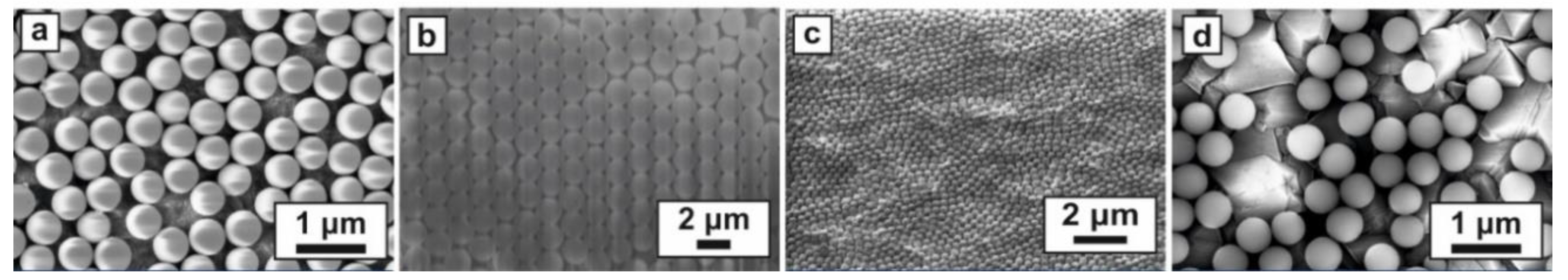
  • Self-assembled mask preparation:
A water-based dispersion of commercial polystyrene (PS) nanospheres with diameters of 500, 1000, and 1500 nm (Microparticles GmbH, Berlin, Germany) mixed with ethanol was deposited using spin-coating (WS-650Sz Lite Single Wafer Spin coater, North Wales, PA, USA) on clean Si substrates or diamond film surfaces. To improve the hydrophilicity of substrates (which helps the spheres spreading evenly), they were treated in oxygen plasma (Tesla 214 VT; 100 W, 60 Pa, 50 sccm, 60 s) before the spin-coating process. The surface wettability was verified using water contact angle measurements.
  • Mask patterning using plasma etching:
Another important point of the study was achieving various templates, that is, tailoring the size and shape of the spheres. The PS mask modification was achieved using reactive ion etching (RIE). A capacitively coupled plasma system (CCP-RIE, Phantom III, Trion Technology, Clearwater, FL, USA) was employed. The etching processes were carried out in oxygen plasma (50 sccm) at a pressure of 12 Pa and radiofrequency (RF) power of 100 W. The monolayers were exposed for various durations (30 s to 2 min) to create diverse arrays of nanofeatures.
  • Mask lift-off:
The spheres are usually used as disposable masks, and they can be removed by sonication in an adequate solvent. In our case, the PS spheres were immersed in toluene or tetrahydrofuran. Similarly, SiO2 spheres were removed using buffered-oxide etching (BOE 7:1, NH4F:HF).
  • Diamond deposition and etching:
The cleaned and nucleated (using ultrasonic seeding with diamond nanoparticles) Si substrates were exposed to different process parameters in order to achieve polycrystalline diamond thin films with various morphology, that is, surface roughness. Micro- or nano-crystalline films were grown on Si substrates in a microwave plasma-enhanced chemical vapour deposition (CVD) reactor (Aixtron P6, Herzogenrath, Germany). Their morphology was controlled by the used gas mixture. The microcrystalline diamond films were grown from a CO2 + CH4 + H2 gas mixture, whereas nanocrystalline diamond films were deposited from a N2 + CH4 + H2 gas mixture. Other process parameters used for the CVD process were as follows: 3 kW, 7 kPa, 800 °C, 1 h [27].
For diamond etching, RIE process (Phantom III, Trion Technology, Clearwater, FL, USA) was used [3]. The etching profiles were tuned using the input process parameters [28]. A suitable disposable etching mask (Au film) was created using evaporation and removed using chemical etching.

3. Results and Discussion

3.1. Fabrication of Diamond Nanostructures Using NSL

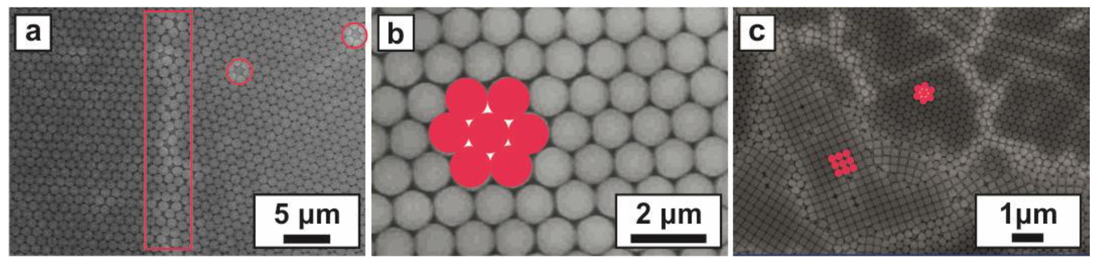
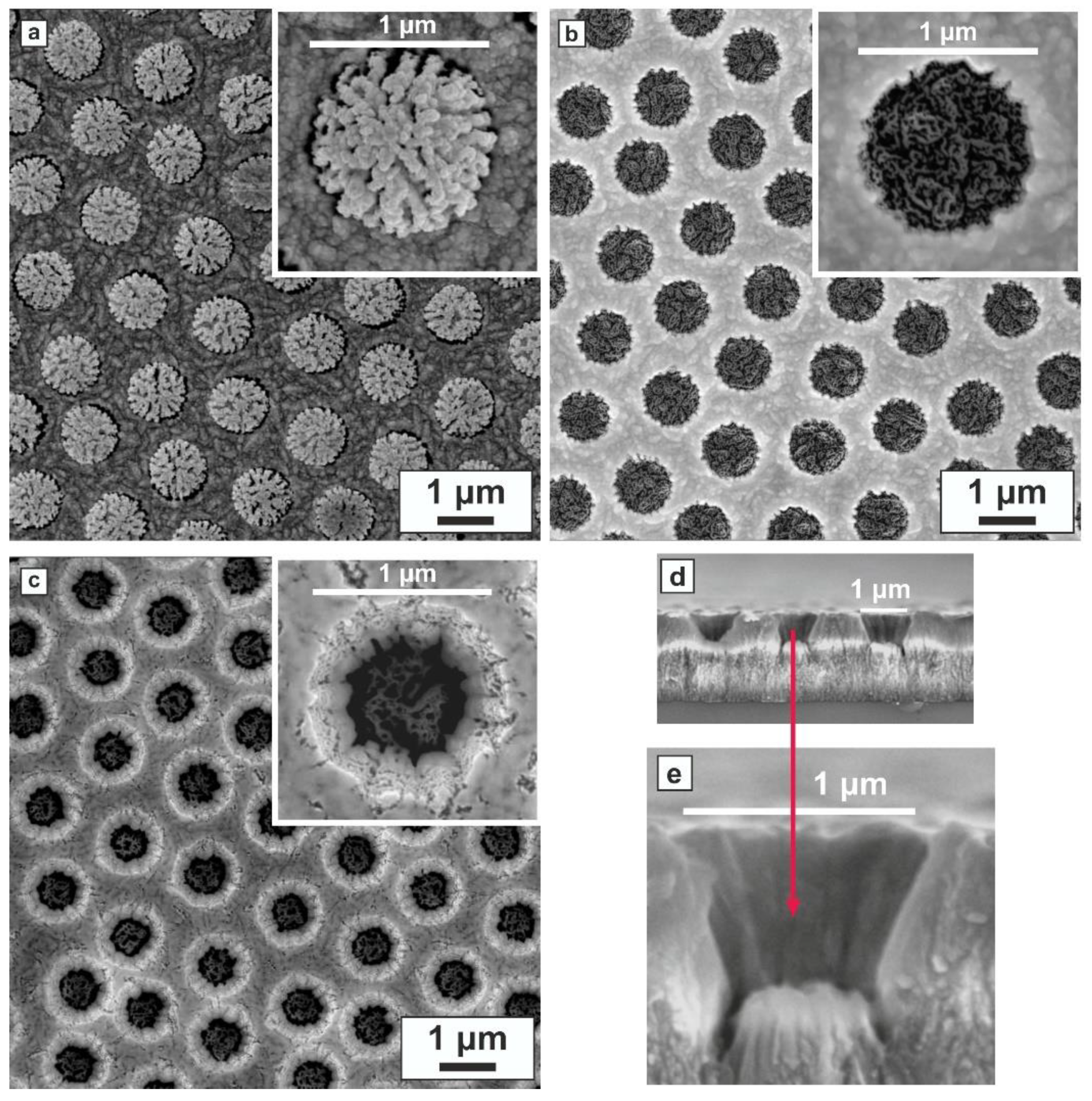
3.1.1. Hexagonal Close-Packed Arrays

The most critical point of the pattering process was the mask preparation step. The wettability of the initial hydrophobic (with a water contact angle larger than 80°) surfaces (Si and polycrystalline diamond thin film) was changed to hydrophilic (with a water contact angle smaller than 10°) using a non-toxic and low-cost oxygen plasma treatment. First, the spin-coating of PS spheres was optimized on smooth surfaces (i.e., Si substrates with root mean square (rms) surface roughness < 1 nm). A crystalline colloidal array with a long-ordered structure exhibits angle-dependent iridescent colour due to the Bragg’s diffraction [31]. This rainbow colour is an immediate indication of the quality of the prepared mask. SEM images (Figure 1a,b) show that the spin-coating resulted in a compact self-assembled monolayer of PS nanospheres (1 µm) under appropriate process conditions, with high surface coverage and without the formation of aggregates (clumping), multilayers, or uncoated areas.
The spheres reached their minimum free Gibbs energy configuration during the spin-coating process, which led to the formation of the colloidal crystals [13]. The self-assembly of PS spheres resulted in a hexagonal close-packed (hcp) array of monolayers (Figure 1b). It is important to note that multilayers exhibited not only hcp ordering but also metastable square packing (Figure 1c) [32]. The success of using colloidal crystals as masks for surface patterning is determined by the quality of the prepared mono/multilayer. The quality of the colloidal crystal lattice is affected by various factors, such as the polydispersity of spheres, dispersion properties, spin-coating process parameters (spinning protocols), and wetting properties of the substrate [33]. It has to be pointed out that crystalline defects are inevitable—dislocations, vacancies, cracks, and other defects (Figure 1a) always emerge in self-assembled masks [29,34].
The compactness of the nanosphere mask also highly depends on the surface roughness of the substrate. Depending on the crystal size and surface roughness, polycrystalline diamond films are divided into micro-, nano-, and ultrananocrystalline diamond [27]. Obviously, the rough surface of the diamond films makes the spin-coating process even more cumbersome. In the case of diamond films, two additional prerequisites had to be fulfilled. First, the diamond film had to consist of crystallites with a fairly uniform size distribution (even more important than the monodispersity of the PS spheres). Individual diamond crystallites, which are much larger than the average crystallite size, can be responsible for defect formation. Second, it is important to apply the appropriate sphere size according to the diamond surface roughness. It is generally proposed that the sphere diameter has to be significantly larger than the average crystallite size of the diamond film (Figure 2a) [9]. In this case, from the point of view of the spheres (e.g., 500 nm or 1 μm), the diamond surface is smooth and uniform enough (e.g., nano- and ultrananocrystalline diamond films with rms roughness < 20 nm, crystal size is below 50 nm) to be coated by a monolayer (Figure 2b).
When the spheres are comparable in size with the diamond crystallites, a monolayer can still be obtained, however, the spheres are already not in one plane, and they follow the initial surface roughness of the diamond film (Figure 2c). Obviously, where the spheres are smaller in size than the individual crystallites of the diamond film it is impossible to create a monolayer on their surfaces. For example, microcrystalline diamond films are composed of large, well-faceted crystals with sizes of up to 500 nm, and the crystal faceting results in high surface roughness values (rms > 50 nm) (Figure 2d). For a more detailed description, see [9,29].
Once acceptable close-packed monolayers are formed on the diamond film, they can be used as the mask for further structuring (see Section 3.3.1). In this study, mask modification (i.e., geometry alteration of nanospheres) using reactive plasma etching was investigated. The permissible degree of disorder (e.g., acceptable level of defects, variation in periodicity) of the prepared lithographic mask depends on the required applications (e.g., optical applications require more precise nanoarrays than sensors) [12].

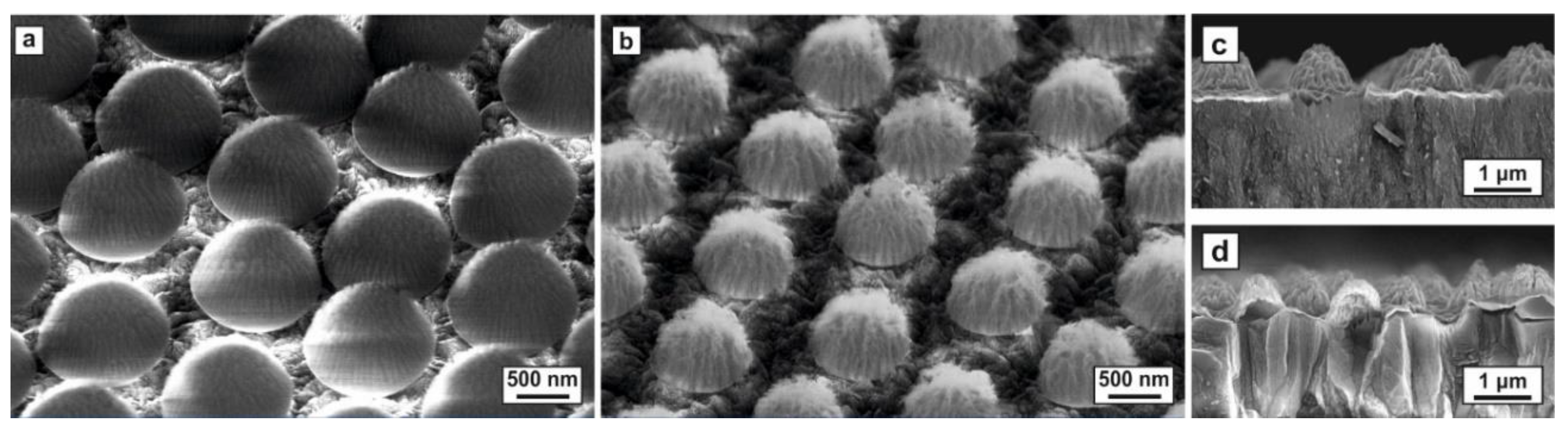
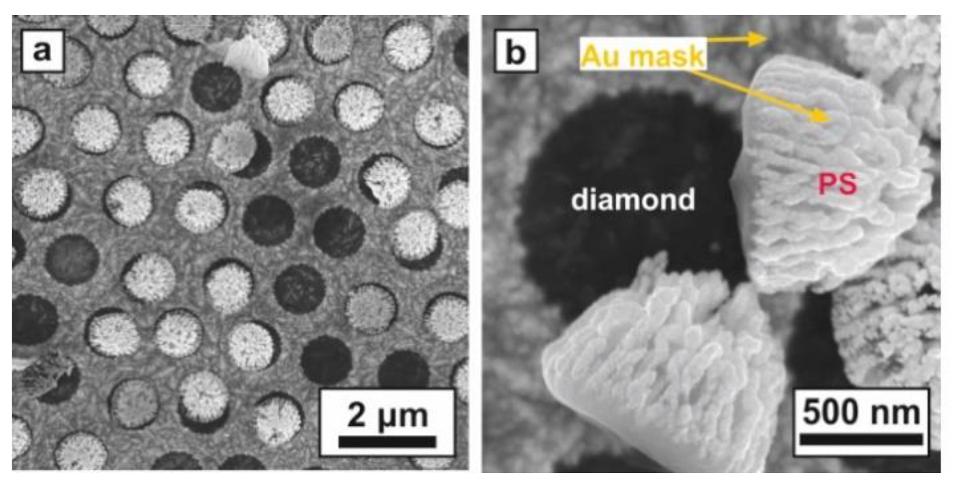
3.1.2. Spherical, Ellipsoidal, and Pyramidal Nanostructures

After the spin-coating process, the PS nanospheres were closely packed into a monolayer with triangular interstices between each triple of spheres (Figure 1b). From these close-packed arrays, non-close-packed arrays (i.e., spheres arranged in a periodic lattice and spaced out equally) were obtained after the reactive ion etching process (Figure 3a,b). The RIE process reduced the size of spheres, changing their shape and surface roughness, but the initial position of their centre (also the periodicity of the array) remained preserved after the plasma treatment. After a short etching time, sphere-like structures were obtained (Figure 3a) with a smooth surface (e.g., PS_1 μm for 30 s, Figure 3a).
Further examples of plasma-etched PS (1.5 μm) monolayers spread on the diamond thin films are demonstrated in Figure 4. From side-view SEM images, it was evident that longer etching durations reduced the PS spheres to non-round shapes. The plasma treatment in the CCP-RIE system was anisotropic, which resulted in the surface roughening and transformation of the spheres into ellipsoidal (Figure 4a—1 min, Figure 4b—1.5 min) or pyramid-shaped (Figure 4c,d—2 min) structures. It can be concluded that various features can be formed by adjusting only the etching duration. For more details about the plasma etching (various systems, the effect of process parameters) of the PS spheres, see [24,25]. The produced non-close-packed monolayers with isolated PS spheres can be used as the mask for further structuring. These kinds of templates are commonly used for nanowire fabrication [24].

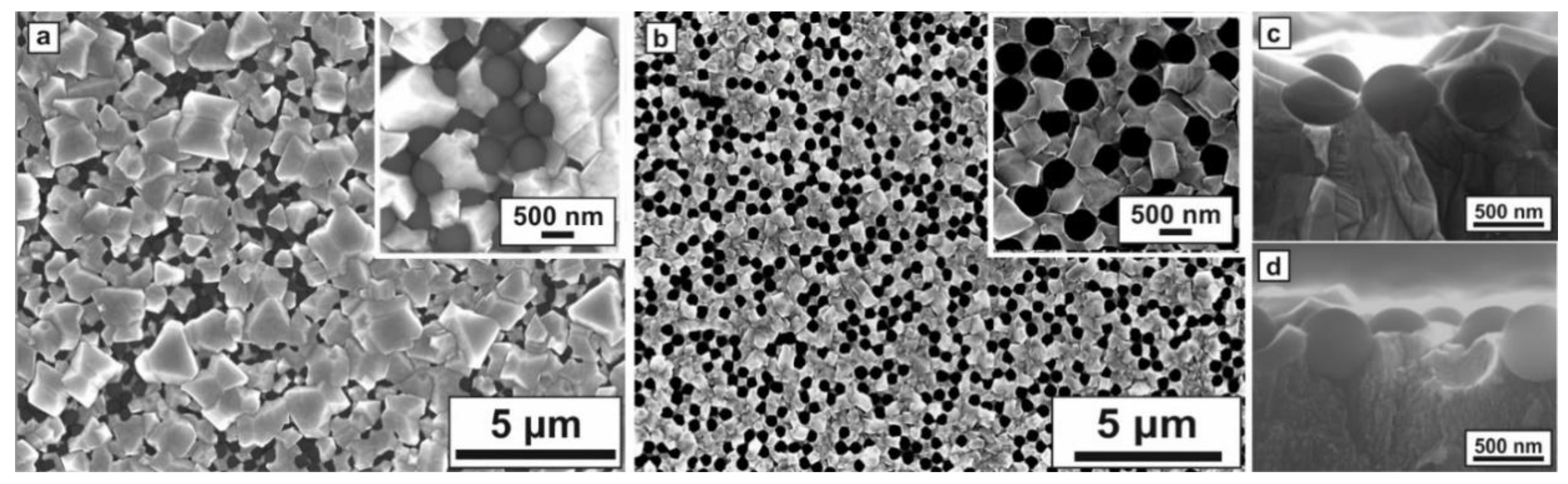
3.1.3. Metallic Nanostructures

Periodic noble metallic nanostructures, which are ubiquitous in nanotechnology (e.g., due to their strong interaction with light through excitation of plasmons), can be also obtained using the NSL method. The unmodified or modified monolayers can be coated by noble metal (e.g., gold, silver, platinum, palladium) films, which result in “metal film over nanosphere” (MFON) structures, which are commonly used as surface-enhanced Raman spectroscopy (SERS) substrates [35]. Other simple and prevalent structures created using NSL are the triangular- and spot-shaped structures. In these cases, unmodified mono- and bilayers are coated with a thin metal layer. The metal fills in areas between the spheres. Then, the desired nanostructures are achieved by removing the PS mask [11]. The periodicity can be adjusted using the diameter of the PS nanospheres.
In our case, a gold layer was deposited over the non-close-packed monolayers (Figure 5, PS_1.5 μm after 2 min etching) at a normal angle (in order to achieve round holes after the lift-off process). The Au layer covered the unprotected region of the diamond films, whereas the area under the PS spheres remained metal-free (i.e., PS masked the diamond surface). The gold layer partially followed the morphology of nanocrystalline diamond film and the surface roughness of the plasma-etched PS spheres.
PS spheres are usually used as a sacrificial mask. In order to achieve holes, the PS spheres were removed using toluene (Figure 5a,b). The lift-off process has to be gentle in order to avoid the peeling of the layers (diamond and Au film) from the substrate. From a practical point of view, the dissolution of PS spheres was observed via naked eye as a white cloud in the Petri dish.
Figure 6 demonstrates other noteworthy geometries of metal nanopatterns formed on nanocrystalline diamond films. In these unorthodox cases, process steps as spin-coating of spheres on nanocrystalline diamond films, modification in linear antenna plasma (combined RF and microwave (MW) plasma) system of the PS mono- and double layers (with hcp or square arrangement), and Au evaporation were employed [25]. For multilayers (3D colloidal crystals), the upper layers act as a shadow mask for the etching of the lower layer [20,36].
With angle-resolved evaporation, it is possible to achieve even more complex nanostructures (rings, crescents, split-rings, asymmetric double split-rings, dimers, etc.), which have a great potential for numerous applications (e.g., metamaterials, plasmonics, photonics, bioscience) [18,20,26,37,38].

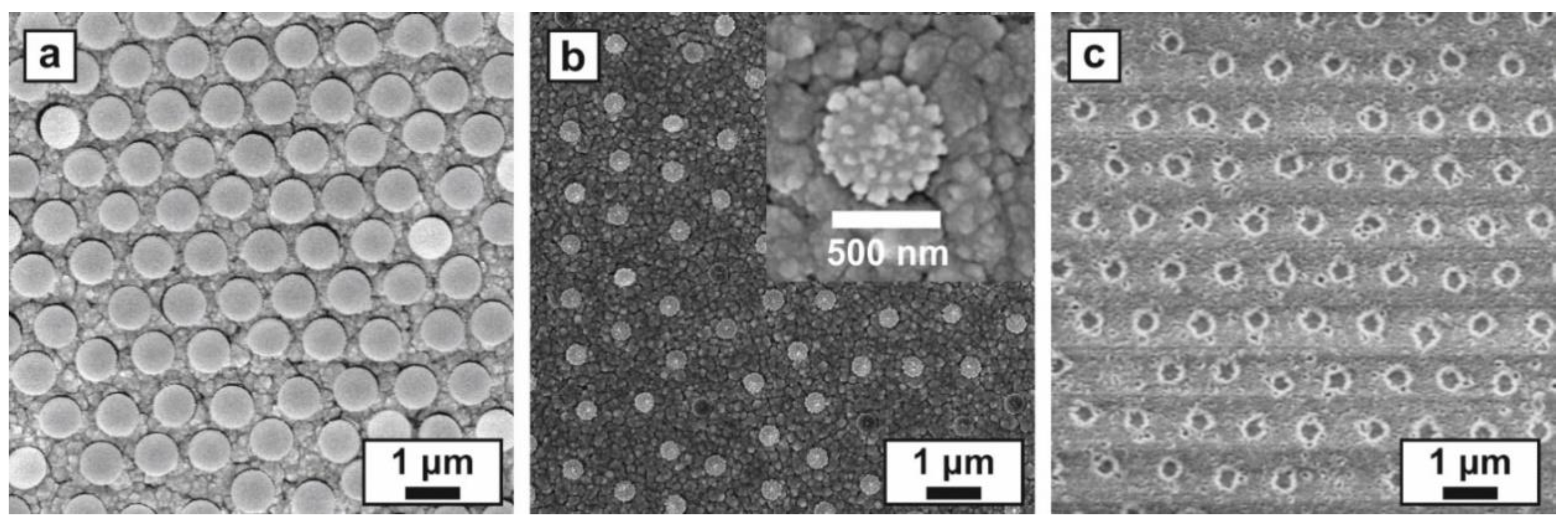
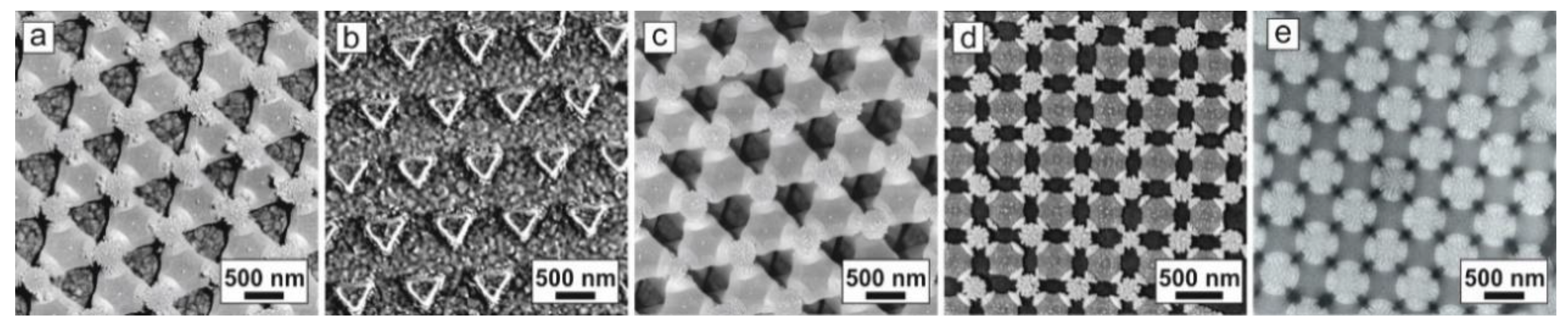
3.1.4. Array of Holes

  • Periodic holes
Optimizing of the above-mentioned individual steps, pre-designed periodic arrays of holes were created in the nanocrystalline diamond film. This intriguing route made use of a dual mask system: (a) hexagonally arranged monolayer of polystyrene spheres and (b) evaporated metal film. This approach was applied to a 1 × 1 cm2 Si substrate. After the CVD diamond growth, PS spheres (with a diameter of 1.5 μm) were spin-coated on nanocrystalline diamond thin films. Their sizes were configured by reactive ion etching, which defined the final diameter of the holes. An oxygen plasma etching (100 W, 12 Pa, 50 sccm, 2 min) induced a reduction of the desired size of the PS spheres (from 1.5 µm to 1 um) while keeping their hexagonally arranged structure. The non-close-packed monolayer of spheres was metal-coated (≈ 80 nm) and used as the shadow masks for the creation of the holes (Figure 7a). After the PS lift-off (ultrasonication in tetrahydrofuran) process (Figure 7b), the diamond was plasma-etched (100 W, 12 Pa, O2/CF4 = 45:2 sccm, 10 min) through the metal mask (Figure 7c). Finally, the Au layer was removed using a chemical etching (in KI/I2-based solution) and periodically ordered arrays of holes (Figure 7c) were fabricated in the diamond film. The diameter, depth, and periodicity of the holes are adjustable on demand. The same fabrication procedure was applied for the sample shown in Figure 3b. In this case, PS spheres with a diameter of 1 µm were reduced to 500 nm and thereby a periodic array of holes with smaller periodicity (as defined by the initial diameter of the PS spheres) and smaller holes were formed (Figure 3c).
  • Unordered pores
Non-periodic structures are obtainable even simpler by employing NSL. In our case, randomly distributed SiO2 spheres with a diameter of 500 nm were spin-coated over the surface of the diamond film (on the Si substrate in size of 1 × 1 cm2). Then, second diamond deposition (conditions: 3 kW, 6 kPa, 3% CH4, 1.5% CO2, 850 °C, 2 h) was performed (Figure 8a), after which the partially overgrown SiO2 spheres were chemically removed with a buffered-oxide etching (BOE 7:1, NH4F/HF) resulting in disordered pores (i.e., openings) in the diamond film (Figure 8b). In this approach, it is technologically required to use SiO2 spheres instead of PS spheres, because PS spheres do not withstand aggressive diamond deposition conditions. Therein, the PS spheres are quickly etched away because of the high temperature and hydrogen plasma during the diamond deposition process [39].
It should be noted that the fabrication steps can be repeated several times in order to achieve pores in the whole volume of the diamond film (ranging from a few hundred nanometres to a few micrometers in thickness). Moreover, the size of the formed pores can be altered by the adequate choice of the initial diameter of the employed spheres.

3.2. Pros and Cons of the Nanosphere Lithography for Diamond Structuring

The structuring of diamond thin films is a viable approach to improve their intrinsic properties and expand the area of applications. However, fabrication of various types of nanostructures (e.g., creation of new morphologies with high aspect ratio, such as holes, whiskers, nanotips, nanocones, nanopillars, columnar structures) in a controlled, reproducible, and precise manner using a simple procedure is a fundamental challenge in nanotechnology [12]. Several important criteria, for instance geometry and morphology control (size, shape, and spacing parameters), area coverage, resolution, cost, and time consumption have to be considered and satisfied for particular cases (Table 1).
Despite all nanofabrication techniques having their own specific benefits, they cannot meet all the requirements of the fabrication process. Using electron beam lithography (EBL) or focused ion beam lithography (FIB), arbitrary patterns, for instance periodic/non-periodic structures with nanometric resolution, are obtained using the scan-based procedure, but they are size-limited and the fabrication process is intrinsically time-consuming [15,40]. These painstakingly precise techniques would be complex and quite expensive (high initial capital and sample processing costs, surface charging, etc.) for applications, which require large area (≈ cm2) nanostructured diamond surfaces [18,22]. These properties of EBL/FIB methods undermine their effectiveness and hamper the mass-production of diamond structures.
NSL mainly takes advantage of the self-assembly phenomenon, which lends itself to large scale fabrication (up to several cm2). For this reason, the creation of certain arrays of nanostructures is relatively simple and affordable [40]. Furthermore, the fabrication process is based on batch operation, and it allows full sample (e.g., spin-coating) or even multiple sample (e.g., etching, deposition) processing [21]. For these reasons, NSL has become a promising and increasingly popular technique in recent years. On the other hand, NSL cannot compete with the impressive spatial resolution of advanced lithography techniques. NSL is also limited in terms of the design of the generated pattern (e.g., arbitrary pattern or independent control of features size and periodicity is not possible) [41]. The major drawback of NSL is the lack of control over defects. The appearance of defects is inevitable because of the self-assembly phenomenon, the non-perfect monodispersity of the spheres, improper process parameters, and surface roughness of the substrate, among other factors. The maximum allowable defect density depends on the requirements that different applications have. The success of nanosphere lithography, this being the precision of the designed nanostructure, is primarily determined by the quality of the lithographic mask.
Directed self-assembly of block-copolymers (BCP) has been used in industrial applications as an alternative pathway for overcoming some issues with NSL and creating more elaborate nanostructures. BCP typically uses lithographically defined topography and chemical contrast to guide the material assembly process. It has pushed the limits of feature size, offering extremely low defectivity and high throughput on large areas with sub-lithographic resolution (≈ 10 nm). BCP has great potential for nanoelectronics devices, energy conversion, and storage [42,43,44].
The aim of this paper was to demonstrate and highlight the usability of NSL for polycrystalline diamond film structuring. As shown above, the fabrication steps of NSL are easily adjustable on demand, and various tailor-made structures can be achieved without the need for complex equipment (see Section 3.1). The periodicity of the structures is controlled by the size of the templating nanospheres. It is possible to use nanospheres with a wide range of sizes (approximately 100 nm to 2 µm), which covers broad waveband (e.g., UV, IR) applications. In this paper, spin-coating was used first as an inherently simple, fast, and repeatable method for producing the mask or colloidal crystals on lab-scale [10,32]. On the other hand, this technique is limited in accuracy and sensitive to the material roughness. It requires tight control over experimental, ambient, and substrate conditions to prevent the formation of major defects, which can be a demanding task. As an effective alternative to spin-coating, a Langmuir–Blodgett trough can be employed to achieve more precise self-assembled monolayers (i.e., hcp monolayers with lower defect density). Another step in NSL attracting much attention is the RIE process, which is the main treatment method used to obtain non-closely packed monolayers. Reactive ion etching was also used in our case to modify the lift-off masks (monolayer of PS spheres) in a controllable and accurate manner. Various traditional and interesting size- and shape-tuneable features (e.g., spherical, ellipsoidal, pyramidal structures with various surface roughening) were easily and successfully obtained. The nanostructure’s design, geometry, and dimension can be estimated by computer simulations for the targeted applications [3,29]. For example, in the case of hole fabrication, it is possible to achieve structures with various thickness (defined by the thickness of the deposited diamond film), hole periodicity (defined by the initial diameter of the spheres), hole diameter (defined by the plasma etching of the PS spheres), and hole depth (defined by the plasma etching of the diamond film). However, the ratio between the hole diameter and the periodicity is not variable arbitrarily. Here, more precise control of diamond etching (e.g., very deep holes with almost vertical sidewalls, high aspect ratio structures, high etching rate, and selectivity) is achievable using deep RIE (e.g., inductively coupled plasma [7]).
In the case of non-periodic structures, the pore diameter was defined by the initial diameter of the spheres, whereas the density of the pores was defined by the spin-coating process parameters (see Section 3.2). The thickness of the porous diamond structure can be adjusted by the thickness of the diamond film or number of fabrication steps (diamond deposition, sphere deposition, and removal). In such an approach, the diamond surface roughness is not a limiting factor because a non-periodic and randomly ordered porous structure is formed. It other words, this approach is also feasible for the porous-like structuring of microcrystalline diamond films because we do not have to consider the ratio between the surface roughness of the diamond films and the diameter of the spheres.

3.3. Potential Applications of Nanostructures Created Using NSL

Up until now, a number of periodic and disordered NSL-based nanopatterned arrays have been designed, fabricated, and utilized on various materials. The approaches presented in this paper produced various arrays of sub-micrometre diamond structures with a predefined shape and dimension, for example, close-packed and non-close-packed monolayers, metal nanostructures, and holes, which may find applications in a variety of important technological fields. In the next section, various ingenious NSL fabrication routes and applications are briefly reviewed to highlight the unexplored potential of NLS structured diamond.

3.3.1. Hexagonal Close-Packed Arrays

Hcp monolayers are commonly used as a mask or template to generate various patterns of functional materials. Zhang et al. achieved a two-dimensional micro/nanohole pattern and three-dimensional hexagonal ring-like array from a PS (1 μm) monolayer using circularly polarized fs laser ablation and chemical etching. These ring-like nanostructure arrays can be applied in lubricant reservoirs, drug delivery, particle trapping, and SERS [46].

3.3.2. Metallic Nanostructures

Metal film over nanospheres prepared using nanosphere lithography is a widely used SERS substrate because of its large, facile, and reproducible SERS properties. Huang et al. created a new type of SERS substrate. They demonstrated that nanoporous gold film over nanospheres (NPGFON) with 3D distributed hot spots generate more than 35 times higher Raman enhancement than conventional gold film over nanosphere (AuFON) structures. They used simple techniques: spin-coating (hcp monolayers from PS spheres with a diameter of 500 and 810 nm), annealing, sputtering, and dealloying. The large SERS enhancement of NPGFON mainly originates from (i) a large surface area (abundant internal nanoporous structures), and (ii) abundant hot spots that locate both near the sharp crevices between adjacent half-domes and in the widely distributed nanopores. They suggest that hot spots mainly originate from the electromagnetic coupling of the widely distributed nanopores and nanogaps. The SERS performance of NPGFON can be adjusted by changing its pore size, gap size, and period [47].
Qi et al. thermally evaporated an Au film on a PS (1 μm) monolayer. Then, the samples were heated in a muffle furnace at different temperatures. The PS spheres vaporized and the metal layer dewetted and formed a nanoparticle array. Using this fabrication procedure, they created a high performance localized surface plasmon resonance (LSPR) sensor, which is a promising label-free sensing technique in biomedical and analytical fields. The location of the narrow LSPR peak can be conveniently manipulated by the thickness of the Au film. They showed a high sensitivity for DNA detection [48].

3.3.3. Arrays of Holes

Nanohole arrays have attracted great interest because of their important technological applications, mainly in plasmonic devices. Xia et al. created a bowl-like pore array made of hollow Au/Ag alloy nanoparticles for SERS detection. These arrays showed a strong SERS performance and detection limit (low to 0.1 ppm) in the detection of melamine molecules in solid milk powder. Their preparation process (hcp PS monolayer colloidal crystal on glass slides, heat treatment, Ag film layer electrodeposition, PS removal, chemical etching) was effective, and the proportion of Ag to Au in the array was adjustable. Such structures are good candidates for SERS application in food safety, biological testing, and so on [49].
Liang et al. developed a plasmonic nanohole-patterned multimode optical fibre probe using the NSL technique with low fabrication cost and high yields. They experimentally investigated sensing performance (bulk refractive index sensitivity and surface sensitivity) and successfully performed a real-time detection/monitoring of specific binding of protein molecules. This type of device is expected to bring exciting opportunities for developing a miniaturized, integrated, and portable biomedical platform [50].
Kahraman et al. created bowl-shaped nanovoid structures, which were coated with a thin Ag layer to obtain plasmonic nanostructures. They used a monolayer of latex spheres (with diameters of 600–1600 nm) as moulds for PDMS. The created nanostructures can be used in plasmonic-based applications (such as sensing, characterization of biological and chemical structures, photovoltaic devices, and catalytic processes) due to their high SERS enhancement factors, large area, simple fabrication procedure, plasmonic tunability (depending on the diameter and the depth of the voids), and mechanical flexibility. The maximum SERS enhancement was obtained using nanovoids with 1400 nm in size (for 785 nm excitation), and 800 nm in size (for 633 nm excitation) [51].
There is a wide range of disordered materials used for photonics (e.g., photonic glass) or plasmonic nanostructures (application in miniaturized analytical and bioanalytical systems, etc.) [32]. Trompoukis et al. fabricated disordered nanostructures by combining NSL (PS sphere width diameter of 170–850 nm) and silicon etching. These structures showed a lower integrated reflectance (8.1%) than state-of-the-art random pyramid texturing (11.7%). When integrated in a 1.1 µm thin crystalline silicon slab, the absorption was enhanced from 24.0% up to 64.3% for the disordered nanopattern. The broadening of resonant modes offers a cost-effective method for integrating advanced light trapping schemes in a solar cell fabrication flow [52].

4. Conclusions

Nanostructures created using NSL have become an important part of nanofabrication and nanoengineering with a wide potential of interest. In this work, the nanosphere lithography method was adapted to polycrystalline diamond thin film structuring. Spin-coating was used as a time-efficient patterning technique, which was further combined with other widespread techniques (plasma etching, metal evaporation, and lift-off). The experimental examples demonstrated that scalable large area nanopatterned diamond arrays prepared using NSL are realistic. Furthermore, the advantages (e.g., increased surface area, diversity, flexibility, uniformity in geometry, large area, reasonably low cost and effort) and some practical issues (e.g., numerous process parameters, defect formation) of the methods were also pointed out for NSL diamond structuring.
We believe that NLS represents a promising method for ingenious designs, and that exploring new procedures for nano-/micro-structuring diamond will open new fields of diamond applications, such as photonic materials [3,22,29,53], Raman or fluorescence plasmonic structures [12,14,18,38], metasurfaces [37,54], biomimetic surfaces (e.g., moth-eye structure) [24], biological and chemical sensors [13,54,55], surfaces with specific wetting properties (e.g., superhydrophobicity, anti-fogging, self-cleaning) [12,19], and many others.

Author Contributions

Data curation, methodology, writing—original draft preparation, M.D.; supervision, writing—review and editing, P.D., A.K. All authors have read and agreed to the published version of the manuscript.

Funding

A.K. acknowledges the Operational Programme Research, Development and Education, financed by European Structural and Investment Funds and the Czech Ministry of Education, Youth and Sports (project no. SOLID21—CZ.02.1.01/0.0/0.0/16_019/0000760); M.D. and P.D. acknowledge the research project SGS19/141/OHK1/3T/11 (Czech Technical University). This work used the large research infrastructure CzechNanolab supported by the LM2018110 project.

Acknowledgments

The authors kindly acknowledge R. Jackivová for SEM measurements.

Conflicts of Interest

The authors declare no conflict of interest.

References

  1. Williams, O. Nanodiamond; Royal Society of Chemistry: Cambridge, UK, 2014; ISBN 978-1-84973-761-6. [Google Scholar]
  2. Karvounis, A.; Nalla, V.; MacDonald, K.F.; Zheludev, N.I. Ultrafast Coherent Absorption in Diamond Metamaterials. Adv. Mater. 2018, 30, 1707354. [Google Scholar] [CrossRef] [PubMed] [Green Version]
  3. Ondič, L.; Varga, M.; Hruška, K.; Fait, J.; Kapusta, P. Enhanced extraction of silicon-vacancy centers light emission using bottom-up engineered polycrystalline diamond photonic crystal slabs. ACS Nano 2017, 11, 2972–2981. [Google Scholar] [CrossRef] [PubMed]
  4. Jeevanandam, J.; Barhoum, A.; Chan, Y.S.; Dufresne, A.; Danquah, M.K. Review on nanoparticles and nanostructured materials: History, sources, toxicity and regulations. Beilstein J. Nanotechnol. 2018, 9, 1050–1074. [Google Scholar] [CrossRef] [PubMed] [Green Version]
  5. Babchenko, O.; Kromka, A.; Hruska, K.; Kalbacova, M.; Broz, A.; Vanecek, M. Fabrication of nano-structured diamond films for SAOS-2 cell cultivation. Phys. Status Solidi 2009, 206, 2033–2037. [Google Scholar] [CrossRef]
  6. Madou, M.J. Fundamentals of Microfabrication and Nanotechnology; CRC Press: Boca Raton, FL, USA, 2012; Volume II, ISBN 978-1-4398-9530-6. [Google Scholar]
  7. Sun, P.; Tang, C.; Xia, X.; Yao, Z.; Quan, B.; Yuan, G.; Gu, C.; Li, J. Controlled fabrication of periodically high-aspect ratio CVD-diamond nanopillar arrays by pure oxygen etching process. Microelectron. Eng. 2016, 155, 61–66. [Google Scholar] [CrossRef]
  8. Kim, J.U.; Lee, S.; Kim, T. Recent advances in unconventional lithography for challenging 3D hierarchical structures and their applications. J. Nanomater. 2016, 2016, 7602395. [Google Scholar] [CrossRef]
  9. Akinoglu, E.M.; Morfa, A.; Giersig, M. Nanosphere lithography-exploiting self-assembly on the nanoscale for sophisticated nanostructure fabrication. Turk. J. Phys. 2014, 38, 563–572. [Google Scholar] [CrossRef] [Green Version]
  10. Zhang, C.; Cvetanovic, S.; Pearce, J.M. Fabricating ordered 2-D nano-structured arrays using nanosphere lithography. MethodsX 2017, 4, 229–242. [Google Scholar] [CrossRef]
  11. Colson, P.; Henrist, C.; Cloots, R. Nanosphere lithography: A powerful method for the controlled manufacturing of nanomaterials. J. Nanomater. 2013, 2013, 948510. [Google Scholar] [CrossRef] [Green Version]
  12. Wang, Y.; Zhang, M.; Lai, Y.; Chi, L. Advanced colloidal lithography: From patterning to applications. Nano Today 2018, 22, 36–61. [Google Scholar] [CrossRef]
  13. Lotito, V.; Zambelli, T. Approaches to self-assembly of colloidal monolayers: A guide for nanotechnologists. Adv. Colloid Interface Sci. 2017, 246, 217–274. [Google Scholar] [CrossRef] [PubMed]
  14. Wang, C.G.; Wu, X.Z.; Di, D.; Dong, P.T.; Xiao, R.; Wang, S.Q. Orientation-dependent nanostructure arrays based on anisotropic silicon wet-etching for repeatable surface-enhanced Raman scattering. Nanoscale 2016, 8, 4672–4680. [Google Scholar] [CrossRef] [PubMed]
  15. Hulteen, J.C.; Treichel, D.A.; Smith, M.T.; Duval, M.L.; Jensen, T.R.; Van Duyne, R.P. Nanosphere lithography: Size-tunable silver nanoparticle and surface cluster arrays. J. Phys. Chem. B 1999, 103, 3854–3863. [Google Scholar] [CrossRef]
  16. Deckman, H.W.; Dunsmuir, J.H. Applications of surface textures produced with natural lithography. J. Vac. Sci. Technol. B 1983, 1, 1109–1112. [Google Scholar] [CrossRef]
  17. Wang, M.; Meng, F.; Wu, H.; Wang, J. Photonic crystals with an eye pattern similar to peacock tail feathers. Crystals 2016, 6, 99. [Google Scholar] [CrossRef] [Green Version]
  18. Wang, Z.; Ai, B.; Möhwald, H.; Zhang, G. Colloidal lithography meets plasmonic nanochemistry. Adv. Opt. Mater. 2018, 6, 1800402. [Google Scholar] [CrossRef]
  19. Kothary, P.; Dou, X.; Fang, Y.; Gu, Z.; Leo, S.-Y.; Jiang, P. Superhydrophobic hierarchical arrays fabricated by a scalable colloidal lithography approach. J. Colloid Interface Sci. 2017, 487, 484–492. [Google Scholar] [CrossRef] [Green Version]
  20. Yu, Y.; Zhang, G. Colloidal lithography. In Updates in Advanced Lithography; Hosaka, S., Ed.; InTechOpen: London, UK, 2013; ISBN 978-953-51-1175-7. [Google Scholar]
  21. Laurvick, T.V.; Coutu, R.A.; Sattler, J.M.; Lake, R.A. Surface feature engineering through nanosphere lithography. J. Micro/Nanolith. MEMS MOEMS 2016, 15, 031602. [Google Scholar] [CrossRef] [Green Version]
  22. Zheng, H.; Ravaine, S. Bottom-Up Assembly and Applications of Photonic Materials. Crystals 2016, 6, 54. [Google Scholar] [CrossRef] [Green Version]
  23. Zhao, X.; Wen, J.; Li, L.; Wang, Y.; Wang, D.; Chen, L.; Zhang, Y.; Du, Y. Architecture design and applications of nanopatterned arrays based on colloidal lithography. J. Appl. Phys. 2019, 126, 141101. [Google Scholar] [CrossRef]
  24. Chen, Y.; Shi, D.; Chen, Y.; Chen, X.; Gao, J.; Zhao, N.; Wong, C.-P. A facile, low-cost plasma etching method for achieving size controlled non-close-packed monolayer arrays of polystyrene nano-spheres. Nanomaterials 2019, 9, 605. [Google Scholar] [CrossRef] [Green Version]
  25. Domonkos, M.; Ižák, T.; Štolcová, L.; Proška, J.; Kromka, A. Controlled structuring of self-assembled polystyrene microsphere arrays by two different plasma systems. In Proceedings of the 5th International Conference NANOCON 2013, Ostrava, Czechia, 16–18 October 2013. [Google Scholar]
  26. Kosiorek, A.; Kandulski, W.; Glaczynska, H.; Giersig, M. Fabrication of nanoscale rings, dots, and rods by combining shadow nanosphere lithography and annealed polystyrene nanosphere masks. Small 2005, 1, 439–444. [Google Scholar] [CrossRef]
  27. Kromka, A.; Babchenko, O.; Potocky, S.; Rezek, B.; Sveshnikov, A.; Demo, P.; Izak, T.; Varga, M. Diamond nucleation and seeding techniques for tissue regeneration. In Diamond-Based Materials for Biomedical Applications; Woodhead Publishing Series in Biomaterials; Narayan, R., Ed.; Woodhead Publishing: Cambridge, UK, 2013; Chapter 9; pp. 206–255. ISBN 978-0-85709-340-0. [Google Scholar]
  28. Domonkos, M.; Izak, T.; Babchenko, O.; Varga, M.; Hruska, K.; Kromka, A. Mask-free surface structuring of micro-and nanocrystalline diamond films by reactive ion plasma etching. ASEM 2014, 6, 780–784. [Google Scholar] [CrossRef]
  29. Domonkos, M.; Varga, M.; Ondič, L.; Gajdošová, L.; Kromka, A. Microsphere lithography for scalable polycrystalline diamond-based near-infrared photonic crystals fabrication. Mater. Des. 2018, 139, 363–371. [Google Scholar] [CrossRef]
  30. Domonkos, M.; Ižák, T.; Štolcová, L.; Proška, J.; Demo, P.; Kromka, A. Structuring of diamond films using microsphere lithography. Acta Polytech. 2014, 54, 320–324. [Google Scholar] [CrossRef]
  31. Lai, C.-F.; Wang, Y.-C. Colloidal photonic crystals containing silver nanoparticles with tunable structural colors. Crystals 2016, 6, 61. [Google Scholar] [CrossRef]
  32. Fang, Y.; Phillips, B.M.; Askar, K.; Choi, B.; Jiang, P.; Jiang, B. Scalable bottom-up fabrication of colloidal photonic crystals and periodic plasmonic nanostructures. J. Mater. Chem. C 2013, 1, 6031. [Google Scholar] [CrossRef]
  33. Chen, J.; Dong, P.; Di, D.; Wang, C.; Wang, H.; Wang, J.; Wu, X. Controllable fabrication of 2D colloidal-crystal films with polystyrene nanospheres of various diameters by spin-coating. Appl. Surf. Sci. 2013, 270, 6–15. [Google Scholar] [CrossRef]
  34. Ye, X.; Huang, J.; Zeng, Y.; Sun, L.-X.; Geng, F.; Liu, H.-J.; Wang, F.-R.; Jiang, X.-D.; Wu, W.-D.; Zheng, W.-G. Monolayer colloidal crystals by modified air-water interface self-assembly approach. Nanomaterials 2017, 7, 291. [Google Scholar] [CrossRef] [Green Version]
  35. Ngo, H.T.; Wang, H.-N.; Fales, A.M.; Vo-Dinh, T. Label-free DNA biosensor based on SERS molecular sentinel on nanowave chip. Anal. Chem. 2013, 85, 6378–6383. [Google Scholar] [CrossRef] [Green Version]
  36. Choi, D.-G.; Yu, H.K.; Jang, S.G.; Yang, S.-M. Colloidal lithographic nanopatterning via reactive ion etching. J. Am. Chem. Soc. 2004, 126, 7019–7025. [Google Scholar] [CrossRef] [PubMed]
  37. Zhao, J.; Frank, B.; Neubrech, F.; Zhang, C.; Braun, P.V.; Giessen, H. Hole-mask colloidal nanolithography combined with tilted-angle-rotation evaporation: A versatile method for fabrication of low-cost and large-area complex plasmonic nanostructures and metamaterials. Beilstein J. Nanotechnol. 2014, 5, 577–586. [Google Scholar] [CrossRef] [Green Version]
  38. Ingram, W.; He, Y.; Stone, K.; Dennis, W.M.; Ye, D.; Zhao, Y. Tuning the plasmonic properties of silver nanopatterns fabricated by shadow nanosphere lithography. Nanotechnology 2016, 27, 385301. [Google Scholar] [CrossRef] [PubMed]
  39. Domonkos, M.; Izak, T.; Stolcova, L.; Proska, J.; Kromka, A. Fabrication of periodically ordered diamond nanostructures by microsphere lithography. Phys. Status Solidi B 2014, 251, 2587–2592. [Google Scholar] [CrossRef]
  40. Acikgoz, C.; Hempenius, M.A.; Huskens, J.; Vancso, G.J. Polymers in conventional and alternative lithography for the fabrication of nanostructures. Eur. Polym. J. 2011, 47, 2033–2052. [Google Scholar] [CrossRef] [Green Version]
  41. Flavel, B.S.; Shapter, J.G.; Quinton, J.S. Nanosphere lithography using thermal evaporation of gold. In Proceedings of the 2006 International Conference on Nanoscience and Nanotechnology, Brisbane, Australia, 3–7 July 2006. [Google Scholar]
  42. Gadelrab, K.R.; Ding, Y.; Pablo-Pedro, R.; Chen, H.; Gotrik, K.W.; Tempel, D.G.; Ross, C.A.; Alexander-Katz, A. Limits of directed self-assembly in block copolymers. Nano Lett. 2018, 18, 3766–3772. [Google Scholar] [CrossRef] [PubMed]
  43. Liu, C.-C.; Franke, E.; Mignot, Y.; Xie, R.; Yeung, C.W.; Zhang, J.; Chi, C.; Zhang, C.; Farrell, R.; Lai, K.; et al. Directed self-assembly of block copolymers for 7 nanometre FinFET technology and beyond. Nat. Electron. 2018, 1, 562–569. [Google Scholar] [CrossRef]
  44. Herr, D.J.C. Directed block copolymer self-assembly for nanoelectronics fabrication. J. Mater. Res. 2011, 26, 122–139. [Google Scholar] [CrossRef]
  45. Aassime, A.; Hamouda, F. Conventional and un-conventional lithography for fabricating thin film functional devices. In Modern Technologies for Creating the Thin-film Systems and Coatings; InTechOpen: London, UK, 2017. [Google Scholar]
  46. Zhang, J.; Wang, S.; Jiang, L.; Wang, M.; Chu, Z.; Zhu, W.; Li, X. Morphology control of nanostructure using microsphere-assisted femtosecond laser double-pulse ablation and chemical etching. Appl. Surf. Sci. 2020, 502, 144272. [Google Scholar] [CrossRef]
  47. Huang, J.; He, Z.; Liu, Y.; Liu, L.; He, X.; Wang, T.; Yi, Y.; Xie, C.; Du, K. Large surface-enhanced Raman scattering from nanoporous gold film over nanosphere. Appl. Surf. Sci. 2019, 478, 793–801. [Google Scholar] [CrossRef]
  48. Qi, X.; Bi, J. Plasmonic sensors relying on nanoparticle arrays created by a template-directed dewetting process. Opt. Commun. 2019, 453, 124328. [Google Scholar] [CrossRef]
  49. Xia, L.; Yang, Z.; Yin, S.; Guo, W.; Li, S.; Xie, W.; Huang, D.; Deng, Q.; Shi, H.; Cui, H.; et al. Surface enhanced Raman scattering substrate with metallic nanogap array fabricated by etching the assembled polystyrene spheres array. Opt. Express 2013, 21, 11349. [Google Scholar] [CrossRef] [PubMed]
  50. Liang, Y.; Yu, Z.; Li, L.; Xu, T. A self-assembled plasmonic optical fiber nanoprobe for label-free biosensing. Sci. Rep. 2019, 9, 7379. [Google Scholar] [CrossRef] [PubMed]
  51. Kahraman, M.; Daggumati, P.; Kurtulus, O.; Seker, E.; Wachsmann-Hogiu, S. Fabrication and Characterization of Flexible and Tunable Plasmonic Nanostructures. Sci. Rep. 2013, 3, 3396. [Google Scholar] [CrossRef] [Green Version]
  52. Trompoukis, C.; Massiot, I.; Depauw, V.; El Daif, O.; Lee, K.; Dmitriev, A.; Gordon, I.; Mertens, R.; Poortmans, J. Disordered nanostructures by hole-mask colloidal lithography for advanced light trapping in silicon solar cells. Opt. Express 2016, 24, A191. [Google Scholar] [CrossRef]
  53. Salomoni, M.; Pots, R.; Auffray, E.; Lecoq, P. Enhancing light extraction of inorganic scintillators using photonic crystals. Crystals 2018, 8, 78. [Google Scholar] [CrossRef] [Green Version]
  54. Zhang, G.; Lan, C.; Bian, H.; Gao, R.; Zhou, J. Flexible, all-dielectric metasurface fabricated via nanosphere lithography and its applications in sensing. Opt. Express 2017, 25, 22038. [Google Scholar] [CrossRef]
  55. Xu, Z.; Wang, L.; Fang, F.; Fu, Y.; Yin, Z. A review on colloidal self-assembly and their applications. Curr. Nanosci. 2016, 12, 725–746. [Google Scholar] [CrossRef]
Figure 1. SEM images of polystyrene (PS) monolayer with hexagonal close-packed (hcp) arrangement (a,b) and mixed-layer consisting of hcp and square-packed (c) PS spheres over Si substrate.
Crystals 10 00118 g001
Figure 2. Representative SEM images of PS spheres on nanocrystalline (ac) and microcrystalline (d) diamond film.
Crystals 10 00118 g002
Figure 3. SEM images of size-reduced PS spheres (a,b) on nanocrystalline diamond film and resulting holes; (c) from the template in image (b)—for details, see Section 3.1.4.
Crystals 10 00118 g003
Figure 4. Representative SEM images of plasma-etched PS spheres over the diamond film (ad).
Crystals 10 00118 g004
Figure 5. Representative SEM images of peeling off of metal-coated PS nanospheres from NCD diamond films (a,b).
Crystals 10 00118 g005
Figure 6. SEM images of multiple kinds of patterns fabricated on nanocrystalline diamond films. Plasma-etched monolayer of PS spheres after Au evaporation (a), and after lift-off the PS spheres (b). Plasma-etched PS mono/multilayers after Au evaporation with hcp (c) and square lattice (d,e).
Crystals 10 00118 g006
Figure 7. Fabrication of periodic array of holes in polycrystalline diamond film. Array of spin-coated polystyrene spheres after plasma etching and Au evaporation (a), PS removal (b), diamond plasma etching through Au mask (c), and cross-section views of holes after Au removal (d,e).
Crystals 10 00118 g007
Figure 8. Spin-coated SiO2 spheres on diamond films (a), and random array of pores in polycrystalline diamond film after removing the spheres (b). Cross-sectional view of microcrystalline (c) and nanocrystalline (d) diamond films.
Crystals 10 00118 g008
Table 1. Several highlighted properties of NSL in comparison with EBL and FIB adapted for diamond structuring [40,45].
CriteriaNSLEBL and FIB
Substrate roughnesslowarbitrary
Mask preparationsimple
(self-assembled mask, batch operation, flat diamond surface favourable)
complex
(direct write technique, surface charging must be compensated on intrinsic diamond)
Patterned arealarge (≈cm2)small (< 1 mm2)
Pattering geometrylimited (in size and shape of mask)arbitrary (almost any shape, size and design)
Time consumptionshort (less than hours for 1 × 1 cm2 )long (around a number of days for 1 × 1 cm2)
Resolutiongoodvery high
Precision and uniformitysatisfactory with defectsextremely high
Defectivityunavoidable defects
(defect-free domains around 10–100 µm2)
extremely low
Costcost-effectivehigh
Throughputhighlow
Repeatability and controllabilitygood
(based on self-assembly)
high
(computer-controlled)
Environmentvacuum requiredclean-room, high vacuum required
Complexity of equipmentsimplecomplicated

