1. Introduction
Photovoltaic cells are a popular source of renewable energy because of their low material cost, environment friendly nature, and renewability. When installing solar cell modules, environmental factors such as the ambient humidity, atmospheric dust, wind speed, and ambient temperature need to be considered [
1,
2]. Therefore, for photovoltaic cells to operate efficiently and universally, it is important to develop solar panels that are contamination-resistant and flexible over the long term. Compared with monocrystalline and polycrystalline silicon, amorphous silicon (a-Si:H) thin-film photovoltaic cells have higher absorption coefficients and can absorb sufficient sunlight to produce high-efficiency photovoltaic cells with a thickness of 500 nm. In contrast, monocrystalline or polycrystalline silicon photovoltaic cells require a thickness of several hundred microns. Therefore, a-Si:H thin-film photovoltaic cells have been attracting attention for a long time, not only because of their low cost, but also because of their potential to be applied on flexible substrates due to their thinness. Although the current efficiency of a-Si:H thin-film photovoltaic cells accounts for approximately 10% [
3], a-Si:H thin-films are prone to having a high defect density, which limits the carrier diffusion length (to 100 nm). Therefore, in the process of making a-Si:H photovoltaic cells, only relatively thin a-Si:H layers can be used, which will reduce the amount of solar light absorbed by the a-Si:H layers.
There are many ways to increase light absorption, among which the use of an anti-reflective layer (ARL) is an important part. A typical a-Si:H thin-film photovoltaic cell uses In
2O
3:Sn (ITO) as the transparent conductive layer. The refractive index of ITO is 1.83, which does not match the refractive index of air (1), thus meaning it has a higher reflectance. Generally, traditional ARLs are made by coating. The most common is a single-layer ARL of one-quarter wavelength thickness. By controlling the thickness and selecting the anti-coating material, the reflected light intensity at a given wavelength can be reduced to approximately 0. However, the above method can only reduce the reflectance of a specific wavelength, meaning the selection of materials that meet this condition is limited. In other studies, multi-layer anti-reflective coatings have been produced. The refractive index shows continuous changes through appropriate film thickness design and selection of the refractive index of each layer, reducing the reflectance and achieving broadband and all-angle anti-reflectance at the same time. Nevertheless, the drawbacks lie in the sophisticated coating process technique that is used, the material diffusion, the thermal expansion mismatch, the small incident wavelength range, and the incident light angle [
4]. The choices of natural materials are limited, especially for materials with a refractive index below 1.83 [
5]. In the past few years, it has been suggested that the subwavelength grating (SWG) of moth-eye pillars has gradually replaced the traditional single- or multi-layer ARLs. The use of subwavelength grating can overcome the limitations of material selection. Because only a single material is used, none of the problems that are commonly seen in the multi-layer anti-reflective coatings occur. Therefore, it is generally accepted that the subwavelength grating approach is more stable and durable than multi-layer anti-reflective coatings for ARL applications. Recently, moth-eye structures have been extensively fabricated using electron beam lithography and dry etching techniques [
6]. However, these technologies will cause the merging of surface defects and reduce the performance of the components. These technologies may not be suitable for mass production of nanostructures on large-area solar cells for commercial purposes. Therefore, many scholars have developed a bottom-up approach to prepare the nanostructures. As a result, many scholars have developed the bottom-up growth method to produce nanostructures.
Zinc oxide is a direct bandgap material of the II–VI group with a direct bandgap of 3.4 eV, with a high transmittance in the visible light range. In addition, zinc oxide also has the characteristics of high electron mobility, non-toxicity, an adjustable refractive index, and easy coating via anisotropic growth. Therefore, ZnO is suitable as an anti-reflective layer material and is rapidly gaining in value [
7,
8,
9,
10]. There are many methods that can be used to grow zinc oxide nanostructures, such as using physical deposition, chemical vapor deposition, and vapor–liquid–solid methods [
11,
12,
13]. However, its production process is expensive. The chemical solution method of growing ZnO nanostructures is promising because of the low technical threshold, mass production capability, low-temperature growth, and low cost as compared with the conventional growth of ZnO nanostructures. There are mainly two methods that are used to improve the light-trapping abilities of amorphous silicon solar cells. In the first method, a nano three-dimensional (3D) topography is prepared on the bottom of the substrate, which then grows the p–n junction solar cell along the nano-3D topography [
14,
15,
16]. Although this method is currently used in many research studies, it is necessary to not only consider the cost of preparing the topography on the substrate, the difficulty of the manufacturing process, and the possibility for commercialization over a large area, but also the fact that the film thickness of the amorphous silicon solar cells prepared using this method will also be affected by the spacing between structures in the nano-3D morphology, easily leading to the Staebler–Wronski effect [
17,
18], which reduces the photoelectric conversion efficiency. The second method uses the wet etching method on the transparent conductive oxide (TCO) to make the surface of the component rough, such that the incident light is scattered into off-normal angles. Therefore, increasing the optical path length in the absorbing layer causes an increase in light absorption. However, this method cannot easily control the surface structure morphology, which limits its future development [
19]. Many studies have reported the use of a ZnO nanostructure for applications in devices. In the past several years, Lai et al. deposited ZnO:Al layers of about 50 nm as the seed layers using the sputtering method, and then using the chemical solution method to grow zinc oxide nanorods with length of about 0.9–2.1 μm, where zinc oxide is mainly used for dye adsorption and carrier transfer [
20]. On the contrary, this paper uses the chemical sol–gel method with spin coating to deposit a ZnO seed layer on the surface of the device, and then uses the chemical solution method to grow zinc oxide nanorods with lengths of about 0.4–2.2 μm, where zinc oxide is used as an anti-reflection layer. Therefore, the production process and functionality of the zinc oxide nanorods in the two papers are different. Shah et al. conducted experiments on the growth of zinc oxide nanorods of different lengths on textured crystalline silicon (c-Si) [
21]. The seed layer solution used was a mixture of zinc acetate hydrate and ethanol, while the spin coating method was used to deposit the seed layer solution on the textured Si wafer. Following this, the chemical solution method was used to grow zinc oxide nanorods with lengths of about 0.75–1.1 μm. The grown zinc oxide nanorods were then annealed at 250 °C for 1 h, obtaining an optimum reflectance of about 10%. The above-mentioned study only prepared and analyzed the characteristics of the anti-reflective layer of zinc oxide nanorods on crystalline silicon. The layer was not actually applied to solar cells, and the characteristics of the devices were only obtained from simulation results. On the contrary, our research method does not require the preparation of a structure for texturization, and the process temperature for the zinc oxide nanorods does not exceed 140 °C. The length of the zinc oxide nanorods can be monitored by simply controlling the growth time to achieve a similar effect of reflectance as mentioned in the literature. In addition, we further applied it to a-Si:H thin-film solar cells to explore the improvement of the hydrophilicity due to the presence of zinc oxide nanorods on the cell surfaces. According to the experimental results, the application of zinc oxide nanorods on the surfaces of a-Si:H thin-film solar cells can not only improve the conversion efficiency, but can also protect the components from external environmental factors.
2. Materials and Methods
Figure 1a shows that very high-frequency, plasma-enhanced chemical vapor deposition (VHF-PECVD) was used to prepare a-Si:H thin-film photovoltaic cells in this study. The deposition sequence involves depositing a p-layer (doped with 10% B
2H
6, thickness of about 12 nm), an intrinsic layer (thickness of 400 nm), and an n-layer (doped with 3% PH
3, thickness of about 20 nm) on the SnO
2:F substrate. The conditions during the deposition were a temperature of 140 °C, frequency of 40 MHz, and a power density of 83 mW/cm
2. Next, a layer of In
2O
3:Sn (ITO) with a thickness of approximately 150 nm was deposited by DC sputtering as a transparent conductive layer. The DC-sputtering-deposited Al was then used as the electrode.
The method used to grow zinc oxide nanorods in this study first involved preparing a seed layer using the sol–gel preparation method, and then using the chemical solution method to grow zinc oxide nanorods. The manufacturing process used for zinc oxide nanorods has been mentioned in many published papers [
22,
23]. Firstly, zinc acetate dihydrate (Zn(CH
3COO
2)·2H
2O, Showa Chemical Industry Co., Ltd., Tokyo, Japan) and ethanol (C
2H
5OH, EtOH, Sigma Aldrich, Tokyo, Japan) were mixed, then the mixture was put into a hot plate magnetic stirrer at 60 °C for 1 h. During the stirring process, mono-ethanolamine (C
2H
7NO, MEA, Acros Organics, Tokyo, Japan) was added and the mixture was stirred continuously at 60 °C for 2 h. The molar concentration ratio of Zn(CH
3COO
2)∙2H
2O to MEA was 1:1. The receiver was placed in an environment at room temperature for 24 h to form a uniform and transparent solution, which was then dropped onto the Si wafer and spun at 3000 rpm for 30 s. The solution was, thus, applied to the Si wafer with the spin coating method, which was then put onto a hot plate and kept at 140 °C for 20 min to allow the component to dry and the seed layer to form. The preparation method for the solution to grow zinc oxide nanorods was as follows. A chemical solution with 0.03 M zinc nitrate (Zn(NO
3)
2.6H
2O, Sigma Aldrich, Tokyo, Japan) and 0.03 M hexamethylenetetramine (C
6H
12N
4, HMT, Sigma Aldrich, Tokyo, Japan) was formed and stirred at room temperature for 20 min. The solution was then poured evenly into different beakers, then the coated seed layer components were placed inside the beakers (with the seed layer facing downward). The beakers were then sealed with aluminum foil and put into an oven set to a temperature of 90 °C for 3–18 h to allow the growth of zinc oxide nanorods (the temperature remained constant during the growth process and the solution did not undergo any changes). The reaction formula for ZnO NRs is as follows:
After growing the zinc oxide nanorods, deionized water was used to clean the surfaces of the components, which were then placed on a hot plate at 100 °C for 30 min to be dried. The morphology, optical properties, and crystal structure of ZnO NRs of different lengths grown on Si substrates were subsequently measured by X-ray diffraction (XRD), field-emission scanning electron microscopy (FESEM), and UV-vis spectrometry (Lambda 900 UV/Visible/NIR). The optimal growth parameters were set for ZnO NRs to grow on the surface of the a-Si:H thin-film photovoltaic cell, as shown in
Figure 1b. The photoelectric conversion efficiency of the a-Si:H thin-film photovoltaic cell was measured under a simulated AM1.5G (100 mW/cm
2). In addition, an external quantum efficiency (EQE) system including a 300 W xenon lamp (Newport 66984) and a monochromator (Newport 74112) was used for the measurements at a fixed temperature of 25 °C. Hydrophilicity was finally measured via the wetting contact angle (WCA) values.
3. Results
Figure 2a–f shows the FESEM sections and top views of ZnO NRs with growth times of 3, 6, 9, 12, 15, and 18 h.
Figure 2g is a graph showing the change trends for the average density, the diameters, and the lengths of zinc oxide nanorods with different growth times. It can be seen from the figure that the longer the zinc oxide nanorods grow, the more the zinc oxide nanorods will increase in length. The corresponding lengths of the zinc oxide nanorods were 3 (0.39 μm), 6 (0.65 μm), 9 (0.94 μm), 12 (1.75 μm), and 15 h (2.18 μm). However, when the growth time reached 18 h, the lengths of the zinc oxide nanorods reduced. This was because long-term growth consumed most of the reactants, thereby changing the concentrations of Zn
2+ and OH-. The concentration of OH- in the solution increased, causing the solution to become alkaline, resulting in the dissolution of ZnO NRs and producing an etch-back effect. Therefore, at the growth time of 18 h, the height of the ZnO NRs began to decline [
24]. The diameters of ZnO NRs only slightly increased as the growth time increased, mainly in the range of 70–75 nm. This increase was attributed to the fact that the growth of ZnO NRs using the chemical solution method was faster in the direction of the vertical substrate. The changes in diameter for ZnO NRs were much slower compared to the changes in length. In terms of density, insignificant variation in the density of ZnO NRs was observed at different growth times.
Figure 3a shows the XRD analysis of ZnO NRs grown on Si substrates at different times. There was only a noticeable signal in the direction of ZnO (002), but no other compound signals. As the growth time was longer, the intensity along the (002) direction tended to grow stronger before becoming weaker at 18 h, presumably due to the shorter lengths of the ZnO NRs.
Figure 3b demonstrates the full-width at half-maximum (FWHM) values calculated for the ZnO (002) planes. The FWHM value was lower as the ZnO NRs became longer, agreeing with results in existing literature [
25].
Figure 3c shows transmission electron microscope (TEM) images of ZnO NRs grown on Si substrates for a growth duration of 15 h. The figure depicts a typical selected-area electron diffraction (SAED) pattern for a single ZnO NR. The SAED pattern shows a diffraction pattern indicating pure single-crystal ZnO, indicating the high quality of the ZnO NRs.
Figure 3d shows the reflectance of ZnO NRs of different lengths at 300–800 nm wavelengths on Si substrates at varying growth times. The average reflectance decreased as the length of the ZnO NRs increased, with the result shown in
Figure 3e. This decrease was caused by an increase in the depth of the surface structure that made the moth-eye effect more pronounced, resulting in a lower reflectance. The ZnO NR with 15 h of growth had the lowest reflectance.
Figure 3f shows the change in the refractive index of a ZnO NR grown for 15 h on the surface of an a-Si:H photovoltaic cell. The reason for the decrease in reflectance for the ZnO NRs grown on the surface of an a-Si:H photovoltaic cell can be explained by the effective medium theory (EMT). The EMT can be used to describe the optical properties of AR structures with multiple ARL stacks [
26,
27]. In the present study, an a-Si:H photovoltaic cell with no ZnO NRs grown on its surface produced a Fresnel reflection due to a drastic change in the refractive index when the air reached the ITO layer, resulting in a loss of incident light. The Fresnel reflection was suppressed with the growth of ZnO NRs on the surface of a-Si:H photovoltaic cells. This suppression was due to the fact that ZnO NRs use different optical interfaces to cause some or even all of the destructive interference to cancel the wavelength, thereby preventing reflection wavelengths. The estimated dimensions of ZnO NRs were obtained from the FESEM image seen in
Figure 2a. We obtained the effective refractive index (n
eff) values of ZnO NRs using the following weighted equation [
28]:
The value of parameter f in this equation is the same as that of the fill factor of ZnO NRs; n
ZnO is the refractive index of the ZnO material, while n
air denotes the refractive index of the air. The refractive index values of air and ZnO are 1 and 2.1, respectively. The fill factor of the ZnO growth density can be calculated from the FESEM image. The calculation results show that the fill factor of ZnO NR nodules is approximately 0.48. Therefore, the n
eff value of a ZnO NR with a height of 2.18 μm in the air is approximately 1.62. The refractive index variation is shown in
Figure 3f. Compared to the a-Si:H photovoltaic cell without ZnO NRs, the refractive index changes more easily, thus suppressing the Fresnel reflection and reducing the incident light loss.
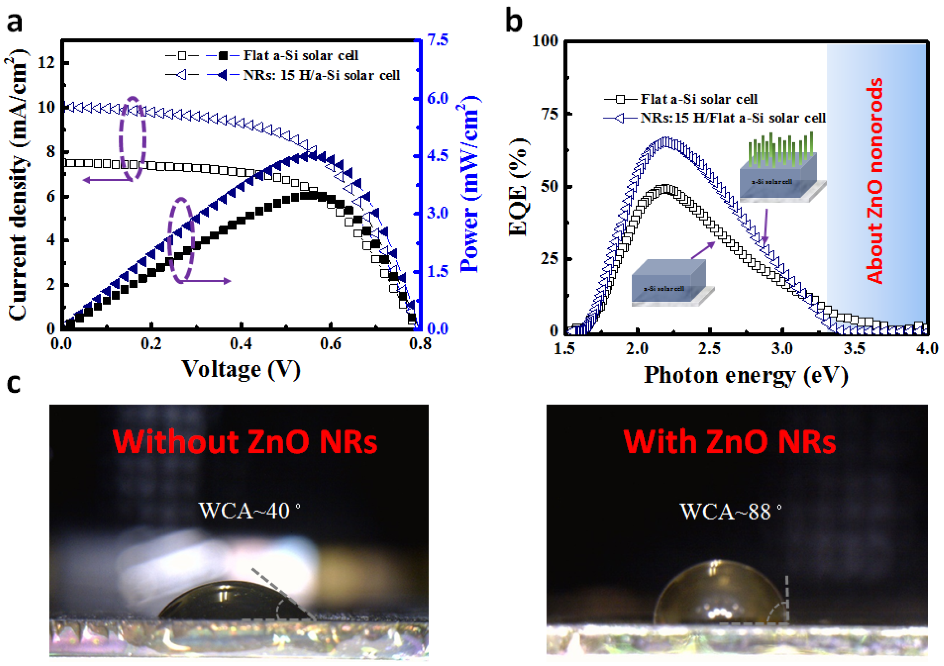
Figure 4a shows the current density–voltage (J-V) curve, comparing the difference between the a-Si:H thin-film bare photovoltaic cell and the a-Si:H thin-film photovoltaic cell with ZnO NRs on the surface.
Table 1 shows the characteristics of the experimental measurements. The conversion efficiencies (η) of the a-Si:H thin-film bare photovoltaic cell and a-Si:H with ZnO NRs were 3.49% and 4.51%, respectively. The open-circuit voltage (V
oc) was approximately 790 mV, the fill factor (F.F.) varied slightly, and the short-circuit currents (J
sc) were 6.23 mA/cm
2 and 8.05 mA/cm
2, respectively. Therefore, the improvement of J
sc was the main reason for the improving efficiency of the a-Si thin-film photovoltaic cells. The photocurrent enhancement factor (EF
jsc) increases by up to 29.2% using the following equation:
In addition,
Table 1 also shows the results of applying the prepared zinc oxide nanorods to monocrystalline and amorphous silicon solar cells in other research studies. It can be seen that Yu et al. first produced the texturization structure, then used a non-vacuum process to grow nanowires with a height of about 100–300 nm to optimize the photoelectric conversion efficiency of the solar cells, improving the optimum photoelectric conversion efficiency by about 3% [
29]. However, during the growth process, the reflectance increased instead when the height of the zinc oxide nanowire columns exceeded 200 nm. This is because zinc oxide nanowires formed a morphology similar to “film”, weakening the anti-reflection effect of the zinc oxide nanostructures. Therefore, in this study, the growth height of the nanowires was limited. Kuang first used a chemical method to grow zinc oxide nanorods of about 400 nm on a flat substrate, and then grew a p–n junction solar cell along the zinc oxide nanorods. Although the photoelectric conversion efficiency increased by about 38.46%, the V
oc and F.F. values significantly decreased, which is disadvantageous in terms of potential component applications [
14]. On the contrary, although the efficiency improvement in this study was slightly lower than that for the amorphous silicon solar cell with zinc oxide nanorods directly grown on the substrate, there was no significant deterioration in the V
oc and F.F. values. In addition, the proposed method achieved a good improvement in the photoelectric conversion efficiency using a relatively simple, highly feasible, and fast manufacturing method. Further optimization of the surface morphology can be achieved in the future, which is of great research value.
Figure 4b shows the EQE measurement results, also demonstrating the increase in η generated by a-Si:H thin-film photovoltaic cells with ZnO NRs on the surface. Compared with the a-Si:H thin-film bare photovoltaic cells, the a-Si:H thin-film photovoltaic cells with ZnO NRs exhibit an enhanced optical response in the range of 1.65–3.1 eV. After 3.1 eV, the EQE values of a-Si:H thin-film photovoltaic cells with ZnO NRs show a drastic decrease, which may be influenced by ZnO NRs. From the EQE measurements, it is indirectly demonstrated that a-Si thin-film photovoltaic cells with ZnO NRs have higher anti-reflective performance, leading to improved J
sc.
Figure 4c shows the WCA measurement results. The WCAs of the unstructured a-Si:H thin-film bare photovoltaic cells and the a-Si:H thin-film photovoltaic cells with ZnO NRs on the surfaces are approximately 40° and 88°, respectively, which suggests that ZnO NRs can reduce the hydrophilicity. When water droplets fall on a low hydrophilic surface, they are more likely to fall off, leaving a clean surface [
30]. This process indicates that environmental influences during the installation of photovoltaic cell modules can be addressed.


