Article

Twinning in Czochralski-Grown 36°-RY LiTaO3 Single Crystals

1
Institute for Materials Research (IMR), Tohoku University, Katahira 2-1-1, Aoba-ku, Sendai 980-8577, Japan
2
Sumitomo Metal Mining Co., Ltd., Suehiro-cho 1-6-1, Ome, Tokyo 198-8601, Japan
3
The Institute of Scientific and Industrial Research (ISIR), Osaka University, 8-1 Mihogaoka, Ibaraki, Osaka 567-0047, Japan
*
Author to whom correspondence should be addressed.
Crystals 2020, 10(11), 1009; https://doi.org/10.3390/cryst10111009
Submission received: 12 October 2020 / Revised: 29 October 2020 / Accepted: 3 November 2020 / Published: 5 November 2020

Abstract

:
The origin of twinning during the Czochralski (CZ) growth of 36°-RY lithium tantalate (LiTaO3) single crystals is examined, and it is shown that lineages composed of dislocation arrays act as an initiation site for twinning. Two types of lineages expand roughly along three different { 1 2 ¯ 10 } planes and two different { 1 1 ¯ 00 } planes. The former lineages and some latter lineages are composed of two types of mixed-dislocations with different Burgers vectors, while the other lineages are composed of only one type of edge-dislocation. All the dislocations have the Burgers vector of ⟨ 1 2 ¯ 10 ⟩ type with the compression side at the +Z side. Twin lamellae on { 10 1 ¯ 2 } are generated at a lineage during the CZ growth. We have hypothesized that dislocations in the lineage with b = 1/3⟨ 1 2 ¯ 10 ⟩ change their extension direction along a slip plane of { 10 1 ¯ 2 }, and they dissociate into pairs of partial dislocations with b = 1/6⟨ 2 2 ¯ 01 ⟩and 1/6⟨ 0 2 ¯ 2 1 ¯ ⟩ forming twin lamellae on { 10 1 ¯ 2 }.

1. Introduction

Lithium tantalate (LiTaO3) crystallizing in the space group R3c [1] represents lithium-based trioxides, and has a unique combination of excellent acoustic, non-linear optical, piezoelectric, pyroelectric, and electro-optical properties depending on its crystallographic direction [2]. The functional crystal is thus the most attractive material for surface acoustic wave (SAW) filters, especially for mobile phones, as well as for frequency conversion [3], acoustic devices [4], and pyroelectric detectors [5,6]. Moreover, the crystal is regarded as a candidate for broadband waveguide quantum memories for entangled photons [7], whispering-gallery-mode resonators with second harmonic generation (SHG) [8], holographic data storage material thanks to its large storage density and high diffraction efficiency [9,10,11], and solid breeder blanket material thanks to its nuclear fusion property [12].
Recently, there is a growing demand for high quality LiTaO3 wafers used for miniaturized SAW filters because of a rapid increase of communication circuits in the telecommunications mobile phone handset market. Nowadays, using Czochralski (CZ) growth techniques [13,14], LiTaO3 single crystals with high optical uniformity, without the macroscopic structural defects of cellular structures, solute striations, domains, and twins [15], can be grown to large diameters more than 4 inches. Even though arrays of dislocations on specific planes (so-called lineages) are occasionally introduced in commercial LiTaO3 single crystals, owing to high thermal stresses during the CZ growth [16], they do not severely influence the performance of SAW filters. Meanwhile, from a commercial point of view, growth of long high-quality CZ-LiTaO3 single crystals is still challenging. One important issue to obtain long CZ-LiTaO3 single crystals is cracking during the growth, because in most cases, such cracked crystals are broken into fragments during the CZ growth and/or wafer processing. Kumaragurubaran has classified the cracking phenomena in CZ-LiTaO3 single crystals into four origins: (1) the crossover of macroscopic twins, (2) change in crystal geometry forming vertexes, (3) ridges, and (4) lineages [17]. Macroscopic twin lamellae on { 10 1 ¯ 2 } planes, which are the predominant cleavage planes [15] and the probable slip planes [18], often nucleate at the bottom part of tantalate crystals during the CZ growth, via the mechanical twinning process [19]. They propagate up to some length in the body, and cracks nucleate when such twins run across one another [17,20,21,22]. Moreover, cracks may be nucleated around the vertex of the angle defined either between the shoulder and the body or between the tail and the body, at which large thermal stress would be generated [23], as well as between the facets at ridges. Those three types of cracking can, however, be suppressed in the commercial CZ-LiTaO3 single crystals by using an appropriate growth condition. Meanwhile, the cracking process at lineages is still unclear. In the present work, we have found that twinning takes place accompanied with cracking at a specific region in which lineages are growing. We have thus determined three-dimensional (3D) distribution and structural properties of the twin domains and lineages to discuss a possible twinning mechanism at lineages.

2. Materials and Methods

Specimens were commercial-grade LiTaO3 single crystals grown by Sumitomo Metal Mining Co., Ltd. (Tokyo, Japan). They were grown from a congruent melt in an iridium crucible in a high frequency induction furnace under a conventional CZ growth condition, thus the non-stoichiometric crystals inevitably introduced a number of point defects (antisites on the lithium sites and cation vacancies). We used a seed for the pulling direction so-called 36°-RY; the direction Y’ was rotated around the X axis of [ 2 1 ¯ 1 ¯ 0 ] by 36° from the Y axis of [ 01 1 ¯ 0 ] towards the Z axis of [0001], which is widely used to obtain commercial LiTaO3 wafers for SAW filters. The orthogonal coordinate system in the crystals can be defined as (X, Y’ (=36°-RY), Z’). The seed was introduced into the melt in a nitrogen and oxygen atmosphere and the temperature was adjusted so as to obtain a stable interface. It was then withdrawn from the melt with simultaneous crystal rotation. The diameter of the crystal, about 4 inches, was controlled by adjusting the furnace temperature automatically. Poling processes were executed after the growth so as to homogenize distributions of composition and point defects, as well as to remove domain reversals in the crystals. Two kinds of LiTaO3 wafers of 0.5 mm thick, both sides of which were polished to a mirror finish by chemical mechanical polishing (CMP) technique [24], were cut out from the single crystals; 36°-RY wafers were cut normal to the pulling direction, and {0001} wafers were cut normal to the Z axis.
A series of 36°-RY wafers was cut out sequentially at equal intervals of 11.8 mm from a crystal, and the distribution of lineages in each wafer was determined by X-ray topography using the Lang method with MoKα1 radiation. A 3D distribution model of lineages in the crystal was then reconstructed by stacking the topographic images sequentially at the interval of 11.8 mm along the 36°-RY direction.
Structural properties of the lineages were examined by transmission electron microscopy (TEM), with a conventional microscope operated at 200 kV (JEOL (Tokyo, Japan), JEM-2000EX), combined with differential interference contrast (DIC) microscopy [25]. A {0001} wafer was cut from a crystal, and it was etched chemically for 15 min in a mixture of HF and HNO3 (1:2) at the temperature of 80 °C [26]. Etch pits of dislocations composing lineages were formed only on the ( 000 1 ¯ ) surface [26]. The surface was observed by DIC microscopy to visualize and analyze the dislocations. A small chip with a specific lineage was then cut from the etched wafer using etch pits as a marker [27], and it was thinned by CMP with colloidal silica in an alkaline solution to obtain electron transparency [28]. TEM specimens except for high-angle annular dark-field scanning TEM (HAADF-STEM) were prepared without ion milling techniques, as the atomistic structure in thin materials, especially in insulators, can be modified during the milling process [29]. Thin foils with a dislocation for HAADF-STEM with a specific incident direction were cut by focused ion beam (FIB) milling. Atomic arrangement around the dislocation was then examined with a JEOL JEM-ARM200F analytical microscope.

3. Results

Most of our non-stoichiometric CZ-LiTaO3 single crystals that are available for commercial wafers contain no macroscopic defect except lineages, and they have high optical uniformity all over the crystals. Very rarely, twinning takes place during the CZ growth and cracks are generated from the twinned region, even though the growth condition for those cracked crystals is similar to that for the crack-free crystals. Twinning takes place at limited regions mostly beneath the ±X surfaces and rarely beneath the –Z’ surface on the cracked crystals (Figure 1). Similar cracking nearby { 2 1 ¯ 1 ¯ 0} surfaces is reported in stoichiometric CZ-LiTaO3 single crystals pulled along the Z axis [16]. The twinned regions are always intersected with lineages, suggesting that lineages would act as initiation sites for twinning.

3.1. Characteristics of Lineages in Single Crystals

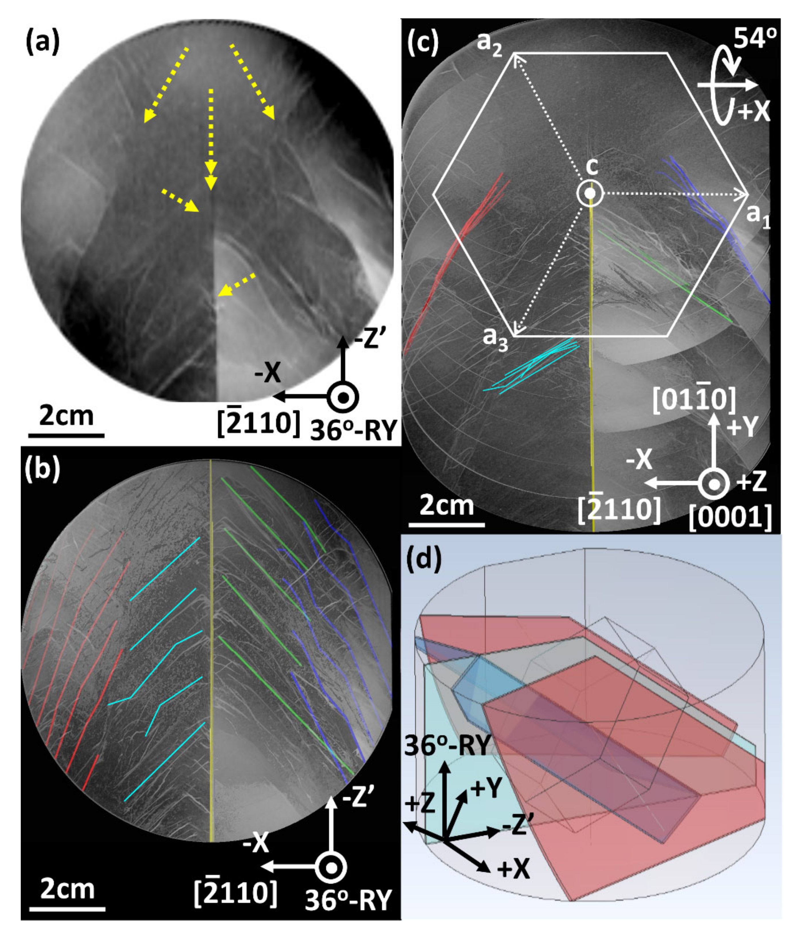
3.1.1. 3D Distribution of Lineages

In a series of 36°-RY wafers cut from single crystals free from cracks and/or twin domains, lineages are observed as almost straight lines by X-ray topography (e.g., Figure 2a). Five kinds of lineages expanding along different planes, of which the location varies in each wafer, are typically observed. Figure 2b shows the reconstructed 3D X-ray topograph of the lineages projected along the pulling direction. Except for the lineage normal to the X axis (indicated with the double arrow in Figure 2a), the other lineages are inclined from the pulling direction. Meanwhile, all lineages are observed edge on when the 3D topograph is observed along the Z axis (Figure 2c), indicating that they are parallel to the Z axis. They would nucleate nearby the +Z’ surface at the vertex of the angle defined between the shoulder and the body, at which large thermal stress would be generated [23]. They expand roughly along three { 1 2 ¯ 10 } planes of ( 1 2 ¯ 10 ), ( 2 1 ¯ 1 ¯ 0 ), and ( 11 2 ¯ 0 ), and two { 1 1 ¯ 00 } planes of ( 1 1 ¯ 00 ) and ( 10 1 ¯ 0 ), as the crystal grows. Those lineages are, therefore, preferentially arranged to form a mirror symmetry to the ( 2 1 ¯ 1 ¯ 0 ) plane passing through the central axis of the crystal, as schematically shown in Figure 2d. This symmetry is the same as the crystallographic symmetry on the 36°-RY plane. Similar 3D distribution of lineages with the mirror symmetry is observed even in the monocrystalline parts in twinned crystals, as shown in Section 3.2.
Comparing X-ray topographs of lineages and optical images of etch pits of dislocations in the same {0001} wafer, each lineage is composed of arrays of dislocations (Figure 3a–f). Two types of lineages can be distinguished by DIC microscopy on etched {0001} wafers. The { 1 1 ¯ 00 } lineages are always observed as double arrays of dislocation etch pits near each other (Figure 3b,f). Meanwhile, the { 1 2 ¯ 10 } lineages are mostly observed as single array of dislocations (Figure 3c–e), and some ( 2 1 ¯ 1 ¯ 0 ) lineages are observed similarly to the { 1 1 ¯ 00 } lineages. The contrast of the etch pits varies depending on the sheared direction. The contrast analysis indicates that the former lineages and some latter lineages are composed of two types of dislocations (Figure 3g), while there is one type of dislocation in the other lineages (Figure 3h). The analysis procedure is summarized in the Appendix A. Structural properties of the dislocations are examined in detail by TEM in the following section.

3.1.2. Structural Properties of Lineages

The ( 1 2 ¯ 10 ) lineage shown in Figure 3c is composed of a set of dislocations arranged at similar intervals of about 5 μm (Figure 4a). The dislocation lines are observable by dark-field (DF-) TEM (e.g., Figure 4b), except when the Burgers vector b is normal to the reflection vector g [30], e.g., for g = [ 1 ¯ 010 ] (Figure 4c) and [ 1 ¯ 012 ] (Figure 4d). The Burgers vector is, therefore, either 1/3[ 1 2 ¯ 10 ] or 1/3[ 1 ¯ 2 1 ¯ 0 ]. This result indicates that the dislocations are not dissociated into pairs of partial dislocations of the 〈 10 1 ¯ 0 〉-type, as observed in some as-grown crystals [31]. Dissociation of dislocations, reported for the dislocations introduced intentionally on (0001) in a LiTaO3 bicrystal [32], is not observed. Dislocations on pyramidal planes with b = 1/3〈 1 ¯ 101 〉 or 1/2〈 2 ¯ 201 〉 (so-called pyramidal dislocations), introduced frequently during the CZ growth with the pulling direction of [0001] [17,18,32,33], are not observed.
The extension directions of the dislocations in the ( 1 2 ¯ 10 ) lineage are determined by stereoscopic BF-TEM. When the incident direction is inclined from [0001] by 50° toward [ 1 ¯ 010 ], each dislocation line is almost parallel to the incident direction (Figure 4e). Besides, Figure 4f shows the dislocation line observed normal to the incident direction, which is inclined from [0001] by 40° toward [ 10 1 ¯ 0 ]. The dislocation line is taken with a negative deviation parameter s with g = [ 1 ¯ 2 1 ¯ 0 ], and its position in the image is displaced to upper side of the dislocation core. This result indicates that b is 1/3[ 1 ¯ 2 1 ¯ 0 ] for the dislocation, because (gb)s < 0 when b is defined by the finish-to-start vector in a right-hand circuit [30]. As schematically shown in Figure 4g, dislocations in the ( 1 2 ¯ 10 ) lineage are edge-type with the compression side at the +Z side in the wafer, and they extend towards the crystal surface as the crystal grows. Dislocations in many { 1 2 ¯ 10 } lineages have similar structural properties, even though the extension direction changes from lineage to lineage.
Figure 5 shows the similar analysis for the ( 1 ¯ 100 ) lineage shown in Figure 3b. The lineage is composed of two sets of dislocations arranged at similar intervals of about 3 μm (Figure 5a). One set of dislocations has the Burgers vector parallel to [ 2 ¯ 110 ], as they are invisible for g = [ 01 1 ¯ 0 ] (Figure 5b) and [ 01 1 ¯ 2 ¯ ] (Figure 5c), while the other set of dislocations has the Burgers vector parallel to [ 1 2 ¯ 10 ], as they are invisible for g = [ 10 1 ¯ 0 ] (Figure 5d) and [ 10 1 ¯ 2 ¯ ] (Figure 5e). Stereoscopic BF-TEM analysis like Figure 4e,f shows that (Figure 5f,g) both dislocations are mixed-type with the compression side at +Z side in the wafer, and they extend the same direction towards the crystal surface as the crystal grows. Those structural properties, schematically shown in Figure 5h, are also obtained from the ( 10 1 ¯ 0 ) lineages and some ( 2 ¯ 110 ) lineages.

3.2. Formation of Twin Lamellae at Lineages

Figure 6a shows an X-ray topograph of a {0001} wafer cut nearby the twinned part in the 36°-RY crystal shown in Figure 1b. The central part of the wafer, which is about 20 mm from the bottom and from the –Z’ surface of the crystal, exhibits white contrast, indicating large lattice distortion. The estimated height of 20 mm from the bottom corresponds with the initiation height at which the beginning of twinning is confirmed by eyes. Several { 2 1 ¯ 1 ¯ 0 } lineages widely expanding towards the –Z surface and short segments of lineages spreading in various directions exist in the distorted part (Figure 6b). The { 2 1 ¯ 1 ¯ 0 } lineages are merged into a single { 2 1 ¯ 1 ¯ 0 } lineage as the crystal grows. We have found that a lamella parallel to the [ 1 2 ¯ 10 ] direction is formed at a { 2 1 ¯ 1 ¯ 0 } lineage nearby the junction of { 2 1 ¯ 1 ¯ 0 } lineages (Figure 6c). The segments of the lineage indicated with the asterisk in Figure 6b are observed as a line, showing that the extension direction of the dislocations composing the segments is not inclined so much with respect to the Z plane, but is nearly parallel to the Z plane. They vary their extension direction just before the formation of the lamella, forming etch pits, and the propagation plane of the lineage is translated to the [ 1 2 ¯ 10 ] direction at the lamella. BF-TEM reveals that some dislocations in the lineage would be connected with the lamella, accompanied by the translation of the lineage.
Figure 7a,b show stereo microscopy of the lamella and lineage shown in Figure 6c, indicating that the lamella propagates on the ( 10 1 ¯ 2 ) plane. Some dislocations in the lineage would propagate on the lamella and their extension direction is close to the growth direction. The other dislocations nearby the lamella also extend to the similar direction. DF-TEM reveals that the Burgers vector of the dislocations on the lamella differs from that of the dislocations observed in single crystals without twinning (i.e., b = 1/3〈 1 ¯ 2 1 ¯ 0 〉). Most of the dislocations on the lamella, indicated by red arrows in Figure 7c, have the Burgers vector nearly normal to [ 2 ¯ 110 ], as they are scarcely observed when g = [ 2 ¯ 110 ] (Figure 7d). Meanwhile, the Burgers vector of the other dislocations, indicated by blue arrows in Figure 7d, is nearly normal to [ 1 ¯ 1 ¯ 20 ], as they are invisible when g = [ 1 ¯ 1 ¯ 20 ] (Figure 7c).
One of the former interface dislocations, with the Burgers vector nearly normal to [ 2 ¯ 110 ], is observed by HAADF-STEM with an FIB specimen. Using DF-TEM, it is confirmed that the Burgers vector and expansion direction of the dislocation would not be modified during FIB milling. HAADF-STEM with the incident direction of [ 1 2 ¯ 10 ], parallel to the lamella, indicates that the lamella is a twin domain with the ( 10 1 ¯ 2 ) twin crystal interface, as observed in Figure 7e. The dislocation line extends towards the right depth direction in the figure. Therefore, although the dislocation line would intersect a specimen surface at the encircled area, it is unclear because the incident direction is not parallel to the dislocation line. In the ( 1 ¯ 012 ) plane indicated with the yellow arrowhead, the atomic columns at the left side of the intersection are arranged on the ( 10 1 ¯ 4 ) planes in the host crystal (as a guide, see the green dotted lines). Meanwhile, those at the right side would be arranged on the ( 10 1 ¯ 4 ) planes in the twin lamella (see the yellow broken lines), indicating an atomic displacement due to the introduction of the interface dislocation. The component of the displacement normal to the twin crystal interface would be negligible. Those results suggest the Burgers vector of the interface dislocation parallel to the twin crystal interface.

4. Discussion

Here, we discuss the formation mechanism of twin lamellae at lineages. TEM reveals that dislocations in a lineage change their extension direction so that they are parallel to the { 10 1 ¯ 2 } plane, and they change their Burgers vector when they are connected with { 10 1 ¯ 2 } twin lamellae. HAADF-STEM suggests that the Burgers vectors would be parallel to the twin interface. According to the pole mechanism of twin formation [34], twins can grow by the movement of a twinning dislocation through successive twinning planes. Considering that { 10 1 ¯ 2 } planes are the probable slip planes in LiTaO3 [18], we hypothesize that dislocations with b = 1/3〈 1 2 ¯ 10 〉 would dissociate into two partial dislocations with b = 1/6〈 2 2 ¯ 01 〉 and 1/6〈 0 2 ¯ 2 1 ¯ 〉 forming a stacking fault on { 10 1 ¯ 2 }. According to the model, the Burgers vector b of the interface dislocations indicated with the red arrows in Figure 7c is parallel to [ 0 2 ¯ 2 1 ¯ ], while that with the blue arrows is parallel to [ 2 2 ¯ 01 ]; i.e., dislocations with b = 1/3[ 1 2 ¯ 10 ], parallel to the twin crystal interface, would dissociate into the interface dislocations. Such an abrupt dissociation of dislocations accompanied with the change of their extension direction may be induced by a stress generated for some reason. Assuming a stress along the radial direction of the crystal r, the Schmid factor of the ( 10 1 ¯ 2 ) slip system for the dislocations with b = 1/6[ 0 2 ¯ 2 1 ¯ ] is quite small, because b is nearly parallel to the growth direction, thus rb ~ 0. On the other hand, the factor for the dislocations with b = 1/6[ 2 2 ¯ 01 ], nearly normal to the pulling direction, is as large as close to 0.5, because the normal direction of the ( 10 1 ¯ 2 ) plane n, almost normal to the pulling direction, is inclined by about 45° with respect to r. This factor is about twice as large as the Schmid factor of the (0001) slip system for the dislocations with b = 1/3[ 1 2 ¯ 10 ] (about 0.3). Therefore, owing to an effect of geometrical arrangement of slip systems in the crystal, undissociated dislocations with b = 1/3[ 1 2 ¯ 10 ] would dissociate into pairs of partial dislocations with b = 1/6〈 2 2 ¯ 01 〉 and 1/6〈 0 2 ¯ 2 1 ¯ 〉. Dislocations with b = 1/6[ 2 2 ¯ 01 ] would move under a stress, leaving dislocations with b = 1/6[ 0 2 ¯ 2 1 ¯ ], and stacking faults between the pairs would expand. Twin lamellae would be formed via the integration of the stacking faults. Similar twin lamellae at lineages are also observed nearby twinned parts in other single crystals, suggesting that twinning at lineages would be an origin of twinning as well as cracking during the CZ growth.
The twinning phenomena takes place in a single crystal even when the growth condition is the same as in the crack-free single crystals. This suggests that the origin of the twinning would not related to the point defects introduced because of non-stoichiometry, even though the defects may impact the threshold stress for twinning. We consider that the stress for twinning would be introduced because of an extrinsic factor irrespective of the normal growth condition, such as an abrupt change of temperature distribution around the crystal/melt interface due to accidental fluctuation of growth temperature, growth speed, and so on. More study is needed to understand how and where the twinning phenomena takes place, towards the control of the generation and growth of twin domains, so as to suppress cracking, by controlling the extrinsic factor.

5. Conclusions

In 36°-RY LiTaO3 single crystals grown by the Czochralski method, five kinds of lineages are introduced during the growth. They would nucleate nearby the +Z surface at the vertex of the angle defined between the shoulder and the body, and expand roughly along three different { 1 2 ¯ 10 } planes and two different { 1 1 ¯ 00 } planes. The { 1 1 ¯ 00 } lineages and some { 1 2 ¯ 10 } lineages are composed of double arrays of mixed-dislocations with different Burgers vectors, while there is only one type of edge-dislocation in the other lineages. All the dislocations have the Burgers vector b of 〈 2 ¯ 10 〉 type with the compression side at the +Z side.
In partially twinned LiTaO3 single crystals, twin lamellae on { 10 1 ¯ 2 } are formed at lineages. We hypothesize the twinning mechanism as follows: (1) undissociated dislocations with b = 1/3〈 1 2 ¯ 10 〉 in a lineage would change their extension direction so that they are parallel to the { 10 1 ¯ 2 } plane, and (2) they are dissociated into two partial dislocations with b = 1/6〈 2 2 ¯ 01 〉 and 1/6〈 0 2 ¯ 2 1 ¯ 〉 forming a stacking fault on { 10 1 ¯ 2 }. Then, (3) twin domains would be formed via the integration of the stacking faults.

Author Contributions

Conceptualization, Y.O.; methodology, Y.O.; validation, Y.O., Y.K., H.Y., T.K. (Toshio Kochiya), and T.K. (Tomio Kajigaya); formal analysis, Y.O.; investigation, Y.O., Y.K., H.Y., T.K. (Toshio Kochiya), and T.K. (Tomio Kajigaya); resources, Y.O.; writing—original draft preparation, Y.O.; writing—review and editing, Y.O.; All authors have read and agreed to the published version of the manuscript.

Funding

This research received no external funding.

Acknowledgments

Conventional TEM was supported by the Laboratory of Alpha-Ray Emitters in IMR, Tohoku University, under the Inter-University Cooperative Research Program in IMR (No. 20M0403). The specimen for STEM was prepared at the Material Solutions Center, Tohoku University. STEM is performed at “Network Joint Research Center for Materials and Devices: Dynamic Alliance for Open Innovation Bridging Human, Environment and Materials” in ISIR, Osaka University (Proposal No. 20201231).

Conflicts of Interest

The authors declare no conflict of interest.

Appendix A

Figure A1 shows a DIC micrograph of etch pits due to the ( 1 2 ¯ 10 ) lineage shown in Figure 3c. In DIC microscopy, a polarized light beam is separated into two orthogonally polarized mutually coherent beams, which are spatially sheared by a specific distance, and the sheared beams illuminate the etch pits. In the present work, the polarization direction of a sheared beam is set to be parallel to the sheared direction. The contrast of the etch pits varies depending on the sheared direction. Comparing the DIC micrographs and TEM data, it is shown that a strong bright contrast appears at the compression side in the etch pits when the Burgers vector of the dislocations is normal to the sheared direction. The bright area in each etch pit is fan-shaped, and the point of the fan would correspond to the dislocation core penetrating the ( 000 1 ¯ ) surface. A similar contrast is obtained from many ( 2 1 ¯ 1 ¯ 0 ) and ( 11 2 ¯ 0 ) lineages when the Burgers vector of the dislocations composing those lineages is normal to the sheared direction.
Figure A2 shows DIC micrographs of etch pits due to the ( 1 1 ¯ 00 ) lineage shown in Figure 3b. Similar to the DIC micrographs of { 1 2 ¯ 10 } lineages, a strong bright contrast appears at the compression side of the etch pits when the Burgers vector of the dislocations is normal to the sheared direction. A similar contrast is also obtained from the ( 10 1 ¯ 0 ) lineage when the sheared direction is normal to the Burgers vector of the dislocations composing the lineage. As a result, using DIC microscopy with different sheared directions, we can examine the Burgers vector and extension direction of the dislocations in both { 1 2 ¯ 10 } and { 1 1 ¯ 00 } lineages in {0001} wafers.
Here, we briefly discuss the origin of the contrast of dislocation etch pits in DIC micrographs. In DIC microscopy, the sheared beams reflected on the specimen are interfered, and this interference induces a contrast [25]. Therefore, the contrast is sensitive to their optical path difference in the sheared direction determined by the geometric path length and refractive index [25]. The etch pit of a dislocation can induce a contrast at an edge when the sheared direction is normal to the edge, because the geometrical path length changes across the edge depending on the 3D shape of the pit, which is determined by strains around the dislocation. In addition, the contrast can vary depending on the polarization direction of a sheared beam when the refractive index is asymmetric. It is known that the refractive index in R3c structures can vary as a result of strains [35]. For edge and mixed dislocations, the sign of the strain component parallel to the Burgers vector at the compressive side is opposite from that at the tensile side. Therefore, the refractive index at the compressive side would differ from that at the tensile side, especially for the polarized beam parallel to the Burgers vector, and this difference can induce an asymmetric contrast on those sides.
Figure A1. (ag) DIC micrographs of dislocation etch pits in a { 1 2 ¯ 10 } lineage at different wafer orientations with respect to the fixed sheared direction, on an etched ( 000 1 ¯ ) surface schematically shown in (h).
Crystals 10 01009 g0a1
Figure A2. DIC micrographs of dislocation etch pits in { 1 1 ¯ 00 } lineages. Most segments are composed of two kinds of dislocation arrays, as in (a), but sometimes those arrays are separated, as in (b).
Crystals 10 01009 g0a2

References

  1. Persson, K. Materials Data on LiTaO3 (SG:161) by Materials Project; Creative Commons: Mountain View, CA, USA, 2014. [Google Scholar] [CrossRef]
  2. Lines, M.E.; Glass, A.M. Principles and Applications of Ferroelectrics and Related Materials; Clearndon Press: Oxford, UK, 1977. [Google Scholar]
  3. Yu, N.E.; Kurimura, S.; Nomura, Y.; Nakamura, M.; Kitamura, K.; Sakuma, J.; Otani, Y.; Shiratori, A. Periodically poled near-stoichiometric lithium tantalate for optical parametric oscillation. Appl. Phys. Lett. 2004, 84, 1662–1664. [Google Scholar] [CrossRef]
  4. Rimeika, R.; Belovickis, J.; Ciplys, D. Leaky-surface-wave generated acoustic beam displacement upon reflection in lithium tantalate crystals. Appl. Phys. Lett. 2013, 102, 031601. [Google Scholar] [CrossRef]
  5. Roundy, C.B.; Byer, R.L. Sensitive LiTa03 pyroelectric detector. J. Appl. Phys. 1973, 44, 929–931. [Google Scholar] [CrossRef]
  6. Glass, A.M.; Abrams, R.L. Study of piezoelectric oscillations in wideband pyroelectric LiTaO3 detectors. J. Appl. Phys. 1970, 41, 4455–4459. [Google Scholar] [CrossRef]
  7. Saglamyurek, E.; Sinclair, N.; Jin, J.; Slater, J.A.; Oblak, D.; Bussieres, F.; George, M.; Ricken, R.; Sohler, W.; Tittel, W. Broadband waveguide quantum memory for entangled photons. Nature 2011, 469, 512–515. [Google Scholar] [CrossRef] [Green Version]
  8. Furst, J.U.; Strekalov, D.V.; Elser, D.; Lassen, M.; Andersen, U.L.; Marquardt, C.; Leuchs, G. Naturally phase-matched second-harmonic generation in a whispering-gallery-mode resonator. Phys. Rev. Lett. 2010, 104, 153901. [Google Scholar] [CrossRef] [Green Version]
  9. Liu, Y.; Kitamura, K.; Takekawa, S.; Nakamura, M.; Furukawa, Y.; Hatano, H. Nonvolatile two-color holographic recording in nondoped near-stoichiometric lithium tantalate crystals with continuous-wave lasers. Appl. Phys. Lett. 2003, 82, 4218–4220. [Google Scholar] [CrossRef]
  10. Yue, X.; Adibi, A.; Hudson, T.; Buse, K. Role of cerium in lithium niobate for holographic recording. J. Appl. Phys. 2000, 87, 4051–4055. [Google Scholar] [CrossRef] [Green Version]
  11. McMillen, D.K.; Hudson, T.D.; Wagner, J. Holographic recording in specially doped lithium niobate crystals. Opt. Express 1998, 2, 491–502. [Google Scholar] [CrossRef] [PubMed]
  12. Naranjo, B.; Gimzewski, J.; Putterman, S. Observation of nuclear fusion driven by a pyroelectric crystal. Nature 2005, 434, 1115–1117. [Google Scholar] [CrossRef]
  13. Ballman, A.A. Growth of piezoelectric and ferroelectric materials by the Czochralski technique. J. Am. Ceram. Soc. 1965, 48, 112–113. [Google Scholar] [CrossRef]
  14. Carruthers, J.; Peterson, G.; Grasso, M. Nonstoichiometry and crystal growth of lithium niobate. J. Appl. Phys. 1971, 42, 1846–1851. [Google Scholar] [CrossRef]
  15. Nassau, K.; Levinstein, H.J.; Loiacono, G.M. Ferroelectric lithium niobate. 1. Growth, domain structure, dislocations and etching. J. Phys. Chem. Solids 1966, 27, 983–988. [Google Scholar] [CrossRef]
  16. Bhagavannarayana, G.; Ananthamurthy, R.V.; Budakoti, G.C.; Kumar, B.; Bartwal, K.S. A study of the effect of annealing on Fe-doped LiNbO3 by HRXRD, XRT and FT–IR. J. Appl. Crystallogr. 2005, 38, 768–771. [Google Scholar] [CrossRef]
  17. Kumaragurubaran, S.; Takekawa, S.; Nakamura, M.; Kitamura, K. Growth of 4-in diameter near-stoichiometric lithium tantalate single crystals. J. Cryst. Growth 2005, 285, 88–95. [Google Scholar] [CrossRef]
  18. Okada, Y.; Iizuka, T. An x-ray topographic study of dislocations in a LiNbO3 crystal. J. Appl. Cryst. 1976, 9, 375–377. [Google Scholar] [CrossRef] [Green Version]
  19. Park, B.M.; Kitamura, K.; Terabe, K.; Furukawa, Y.; Ji, Y.; Suzuki, E. Mechanical twinning in stoichiometric lithium niobate single crystal. J. Cryst. Growth 1997, 180, 101–104. [Google Scholar] [CrossRef]
  20. Vere, A.W. Mechanical twinning and crack nucleation in lithium niobate. J. Mater. Sci. 1968, 3, 617–621. [Google Scholar] [CrossRef]
  21. Park, B.M.; Kitamura, K.; Furukawa, Y.; Ji, Y. Relation between mechanical twinning and cracking in stoichiometric lithium niobate single crystals. J. Am. Ceram. Soc. 1997, 80, 2689–2692. [Google Scholar] [CrossRef]
  22. Yang, J.; Sun, J.; Xu, J.; Li, Q.; Shang, J.; Zhang, L.; Liu, S.; Huang, C. Twin defects in thick stoichiometric lithium tantalate crystals prepared by a vapor transport equilibration method. J. Cryst. Growth 2016, 433, 31–35. [Google Scholar] [CrossRef]
  23. Louchev, O.A.; Kumaragurubaran, S.; Takekawa, S.; Kitamura, K. Thermal stress inhibition in double crucible Czochralski large diameter crystal growth. J. Cryst. Growth 2004, 274, 307–316. [Google Scholar] [CrossRef]
  24. Moriyama, K.; Ozeki, A.; Haba, S.; Mori, M. The Effect of Slurry pH and Particle Size on LiTaO3 Polishing. Technical Paper of Nitta DuPont Incorporated. 2017. Available online: https://www.nittadupont.co.jp/en/technical/692/ (accessed on 1 October 2020).
  25. Murphy, D. Differential Interference Contrast Microscopy and Modulation Contrast Microscopy in Fundamentals of Light Microscopy and Digital Imaging; Wiley-Liss: New York, NY, USA, 2001; pp. 173–198. [Google Scholar]
  26. Ohno, Y.; Kubouchi, Y. Analysis method for dislocations in lithium tantalate. JPN Patent Application 2018-013246, 30 January 2018. [Google Scholar]
  27. Ohno, Y.; Tajima, K.; Kutsukake, K.; Usami, N. Generation of dislocation clusters at triple junctions of random angle grain boundaries during cast growth of silicon ingots. Appl. Phys. Express 2020, 13, 105505. [Google Scholar] [CrossRef]
  28. Ohno, Y.; Taishi, T.; Bamba, N.; Yonenaga, I. Microstructure of striae in <04-41>-oriented lithium niobate single crystal grown by Czochralski method. J. Cryst. Growth 2014, 393, 171–174. [Google Scholar] [CrossRef]
  29. Ohno, Y.; Yoshida, H.; Kamiuchi, N.; Aso, R.; Takeda, S.; Shimizu, Y.; Nagai, Y.; Liang, J.; Shigekawa, N. Impact of focused ion beam on structural and compositional analysis of interfaces fabricated by surface activated bonding. Jpn. J. Appl. Phys. 2020, 59, SBBB05. [Google Scholar] [CrossRef]
  30. Williams, D.B.; Carter, C.B. Transmission Electron Microscopy; Plenum Press: New York, NY, USA; London, UK, 1996; pp. 441–481. [Google Scholar]
  31. Peter, A.; Fries, E.; Riviere, J.P. TEM observation of plastically induced dislocations in lithium niobate LiNbO3 single crystals. Phys. Status Solidi A 1991, 128, 45–53. [Google Scholar] [CrossRef]
  32. Furushima, Y.; Nakamura, A.; Tochigi, E.; Ikuharpa, Y.; Toyoura, K.; Matsunaga, K. Dislocation structures and electrical conduction properties of low angle tilt grain boundaries in LiNbO3. J. Appl. Phys. 2016, 120, 142107. [Google Scholar] [CrossRef]
  33. Cerva, H.; Pongratz, P.; Skalicky, P. Lattice defects in single-crystal lithium niobate I. transmission electron microscopy. Philos. Mag. A 1986, 54, 185–197. [Google Scholar] [CrossRef]
  34. Cottrell, A.H.; Bilby, B.A. LX. A mechanism for the growth of deformation twins in crystals. Philos. Mag. 1951, 42, 573–581. [Google Scholar] [CrossRef]
  35. Eknoyan, O.; Taylor, H.F.; Tang, Z.; Swenson, V.P.; Marx, J.M. Strain induced optical waveguides in lithium niobate, lithium tantalate and barium titanate. Appl. Phys. Lett. 1992, 60, 407–409. [Google Scholar] [CrossRef]
Figure 1. 36°-RY LiTaO3 single crystals in which twinning takes place beneath (a) +X and (b) −Z’ surfaces. The visible twinned region in each crystal is indicated with the rounded rectangle.
Crystals 10 01009 g001
Figure 2. (a) X-ray topograph of lineages in a 36°-RY wafer cut from a 36°-RY single crystal. Reconstructed 3D X-ray topograph of lineages projected parallel to (b) 36°-RY and (c) [0001] directions. (d) Schematic view of the 3D distribution of lineages in the crystal.
Crystals 10 01009 g002
Figure 3. (a) X-ray topograph of lineages in a {0001} wafer cut from a 36°-RY single crystal. Typical etch pit patterns of lineages propagating on (b) ( 1 1 ¯ 00 ), (c) ( 1 2 ¯ 10 ), (d) ( 2 ¯ 110 ), (e) ( 11 2 ¯ 0 ), and (f) ( 10 1 ¯ 0 ). These data are obtained from the regions indicated in (a). Differential interference contrast (DIC) micrographs of dislocation etch pits in (g) ( 1 1 ¯ 00 ) and (h) ( 1 2 ¯ 10 ) lineages taken with the sheared direction shown in each figure.
Crystals 10 01009 g003
Figure 4. (a) Low magnified bright-field (BF-) transmission electron microscopy (TEM) image of a { 1 2 ¯ 10 } lineage. (bd) Dark-field (DF)-TEM images of the dislocation in the square in (a), taken with g indicated in each figure. (e and f) Stereoscopic BF-TEM images of the dislocation, taken with g = [ 1 ¯ 2 1 ¯ 0 ] and s < 0 with the incident direction indicated in each figure. (g) Schematic view of the { 1 2 ¯ 10 } lineage in (a).
Crystals 10 01009 g004
Figure 5. (a) Low magnified BF-TEM image of a {1-100} lineage. (be) DF-TEM images of the dislocations in the square in (a), taken with g indicated in each figure. (f and g) Stereoscopic BF-TEM images of the dislocations, taken with g = [ 1 ¯ 100 ] and s < 0 with the incident direction indicated in each figure. (h) Schematic view of the { 1 1 ¯ 00 } lineage in (a).
Crystals 10 01009 g005
Figure 6. (a) X-ray topograph of lineages near the twinned part in the crystal shown in Figure 1b. The wafer is cut nearby the twinned region, indicated by the red line in the right figure. (b) Etch pit patterns of lineages obtained at the strained region shown in (a). (c) A lamella intersecting a lineage is observable in the squared region shown in (b). (d) BF-TEM of the lamella and lineage in the squared region shown in (c).
Crystals 10 01009 g006
Figure 7. (a,b) Stereo micrographs of dislocations around the lamella shown in Figure 6d. The incident directions are (a) nearly parallel to the growth direction and (b) along the Z axis. (c and d) DF-TEM images of the dislocations on the lamella, taken with g indicated in each figure. (e) High-angle annular dark-field scanning TEM (HAADF-STEM) image of a dislocation on the lamella taken with the incident direction of [ 1 2 ¯ 10 ].
Crystals 10 01009 g007
Publisher’s Note: MDPI stays neutral with regard to jurisdictional claims in published maps and institutional affiliations.

