Abstract
This brief proposes a signal-independent background calibration in pipeline-SAR analog-to-digital converters (ADCs) with a convergence-accelerated technique. To achieve signal independence, an auxiliary capacitor array CA is introduced to pre-inject a pseudo-random noise (PN) in the sampling phase to cancel out the opposite PN injection of the calibrated capacitor in the conversion phase, and CA is also used to realize the D/A function of the calibrated capacitor in the conversion phase. In this way, no matter what the signal is, the residue headroom remains unchanged even with PN injection. Moreover, the first sub-ADC is designed with extended conversion bits to quantize its own residue after delivering the conversion bits required by the first stage. Afterwards, this result is provided to the calibration algorithm to reduce the signal component and accelerate the convergence. Based on the simulation, the signal-to-noise and distortion ratio (SNDR) and spur-free dynamic range (SFDR) improve from 45.3 dB and 56.4 dB to 68.2 dB and 88.4 dB, respectively, after calibration. In addition, with the acceleration technique, convergence cycles decrease from 1.7 × 10⁸ to 5.8 × 10⁶. Moreover, no matter whether the input signal is DC, sine wave or band-limited white noise, the calibration all works normally.
1. Introduction
The successive approximation register analogue-to-digital converter (SAR ADC) is the most power- and area-efficient architecture to attain 8~12-bit resolution [1,2], while its conversion speed is limited due to the inherent serial conversion process. The pipeline-SAR ADC splits the SAR ADC into two stages and connects them with an amplifier to realize pipelined operation, not only reducing conversion time, but also suppressing the comparator noise [3,4]. However, the induced inter-stage gain error and inevitable capacitor mismatch error cause bit-weight errors and, thus, degrade ADC performance. Foreground calibration can extract those errors and compensate them in the digital or analog domain, but cannot track environment variation and thereby requires a high-gain amplifier [5], such as the ring amplifier [6] or telescopic amplifier, which are power-hungry and have complex structures. Background calibration can track the gain variation of the amplifier and allows employing a power-efficient open-loop amplifier, such as the dynamic amplifier [7,8] or gm-R amplifier [9] in pipeline-SAR ADCs. The signal-dependent background calibration is facilitated by detecting the signal value and injecting PNs correlated with the bit-weight errors into the residue path [10]. The correct bit weights can be achieved by exploiting the least mean square (LMS) iterative algorithm, which only involves addition and shift operations. Nevertheless, the signal dependence causes failure of the calibration when the input signal is DC or has a small dynamic range. In [11], the foreground and signal-independent background calibration are adopted to treat capacitor mismatch and inter-stage gain error, respectively, but the demand of multi-bit multiplication and division operation to update bit weights makes the method complex. Moreover, the signal independence increases the signal interference and, thus, decreases the algorithm’s convergence speed. The split-ADC calibration [12], where the ADC is divided into two identical half-ADCs to convert the input signal into different paths, exploits the outputs’ difference to eliminate the signal interference, and, therefore, increases the convergence speed, although it incurs more area and power consumption since the parasitic effect and logic circuit almost double. Sharing the first stage with two second stages in [13] achieves the same acceleration effect as split-ADC, but the residue requires two amplifications, which reduces the ADC speed.
In this brief, a signal-independent background calibration with short convergence time is implemented by introducing an auxiliary capacitor array and modifying the sub-ADC structure. To realize signal independence, PN is pre-injected into an auxiliary capacitor array CA in the sampling phase to counteract the opposite PN injection of the calibrated capacitor in the conversion phase, and CA is also used to realize the D/A function of the calibrated capacitor in the conversion phase. Using a coarse sub-ADC to convert the first stage’s result into pipeline-SAR ADC can not only improve speed and power, but also loosen the reference voltage settling [14,15]. The calibration modifies the sub-ADC with extended conversion bits to quantize its own residue after delivering the conversion bits required by the first stage. Afterwards, this result is provided to the calibration algorithm to reduce signal interference and accelerate the convergence.
2. Proposed Background Calibration
The block diagram of the proposed pipeline-SAR ADC is shown in Figure 1a with single-end structure, while the actual design is differential. The two stages are configured as 5 bits and 8 bits with 1-bit redundancy, and the inter-stage gain is 8 instead of 16 for reducing the amplifier output swing. The four most significant bits (MSBs) of the 1st stage are thermometer-coded and the least significant bit (LSB) is binary, and they comprise the 1st stage main DAC for generating the residue after SAR conversion. An auxiliary capacitor array CA whose value is equal to one MSB unit capacitor is introduced to the 1st stage CDAC for working alternatively with the main DAC’s capacitor that PN is injected into. The values of the 1st stage CADC are depicted in Figure 1a, in which CM15ߝCM0 and CA3–CA0 represent the main DAC capacitors and the auxiliary capacitors, respectively, while C5–C1 refer to capacitors corresponding to the 5 bits of the 1st stage. An 8-bit sub-ADC is implemented and configured as 5 + 4 bits with 1-bit redundancy, and the 5 bits are delivered to the 1st stage CDAC for generating residue while the 4 bits are transmitted to the calibration engine for speeding up calibration. The timing diagram is illustrated in Figure 1b. The sub-ADC attains the 4-bit conversion results used for acceleration when the 1st stage’s residue is amplified, which does not reduce ADC speed. Since the noise in sub-ADC does not affect the main ADC’s outputs for its redundancy, the sampling capacitors occupy a small area and the comparator is low-power. Nonetheless, the residue of the 1st stage and sub-ADC after 5 MSBs’ conversion are not equal due to the capacitors’ mismatch, and will limit the signal elimination effect. In Section 3, Monte Carlo simulations are performed to evaluate the negative effect.
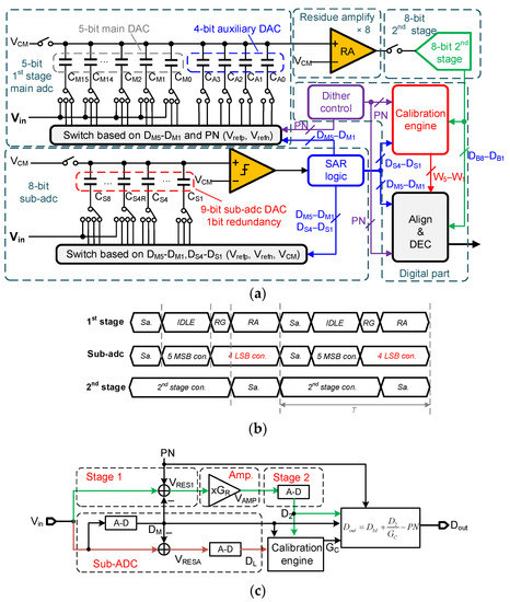
Figure 1.
(a) Block diagram, (b) timing diagram and (c) simplified signal flow diagram of the proposed pipeline-SAR ADC.
The simplified signal flow diagram is illustrated in Figure 1c. Firstly, the input signal Vin is sampled by both the 1st stage and sub-ADC as in [14]. Then, the sub-ADC converts Vin into 5-bit digital results, DM, that are subtracted from Vin in the 1st stage and sub-ADC simultaneously to obtain the residue voltage VRES1 and VRESA, respectively. Furthermore, PN is added to the 1st stage’s VIN for extracting inter-stage gain [10]. Afterwards, VRES1 is amplified GR times and the amplified voltage VAMP is converted by the 2nd stage into 8-bit D2. Meanwhile, the residue VRESA is converted into 4-bit DL by sub-ADC. After that, DM, DL and D2 are passed to the calibration engine to attain the calibrated gain Gc. Finally, the digital part utilizes DM, DL and GC to achieve the 12-bit output Dout.
2.1. Signal-Independent PN Injection
For extracting the bit weights, PN should be correlated with the capacitors of the 1st stage SAR DAC (C5-C1). However, C5-C1 should be connected to DM5-DM1, the 5 MSBs’ conversion results of sub-ADC, to generate the 1st stage residue. To resolve this problem, the auxiliary capacitor CA is introduced to replace the injected part to generate residue.
C5-C2 change to thermometer code CM15-CM1 so that CA can be 2Cu instead of 16Cu to save area. Nevertheless, the residue also increases due to the injection and saturates the 2nd stage. An opposite PN is pre-injected into CA to cancel out residue change. Consequently, PN can be injected into any one of CM15-CM1 whatever the signal is. Taking CM1 as an example, Figure 2 shows how PN is injected into CM1. During the sampling phase, PN is sampled on the bottom plate of CA3-CA0, and Vin is sampled on the bottom plate of CM15-CM0. After sub-ADC finishes 5 MSBs’ conversion, the residue-generating phase comes, and CA3-CA0 are connected to DM2 while CM1 is connected to PN. The residue Vres on the top plate can be derived as
where Vref denotes the reference voltage and Ct refers to the total value of CM15-CM0. Equation (1) shows PN is injected into CM1-CA. If there is no mismatch between CM2 and CA, the residue is
which indicates that PN injection is canceled out and the residue remains unchanged.
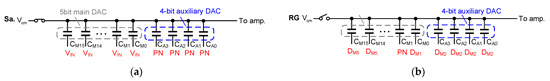
Figure 2.
The connection configurations of the 1st stage CDAC when PN is injected into CM1 (a) in sampling phase; (b) in residue generation phase.
In fact, only the values of CM1-CA can be obtained after calibration, and CA should be measured first. CA is divided into CA3~CA0 for reducing the residue range overhead during PN injection. Table 1 shows the detailed PN injection configurations, where only CM1 is listed because CM15-CM1 are similar. PNs are injected into CA0, CA1-CA0, CA2-CA1-CA0, CA3-CA2-CA1-CA0, CM1-CA3, CM0-CA, respectively, and CA3~CA0 and CM1~CM0 are obtained by adding those delta values. The maximum residue range is [−1.25, 1.25] LSB when PN is injected into CA0, and there is still a 0.75-bit redundancy left of the 2nd stage quantization range.

Table 1.
PN Injection in the First Stage CDAC.
2.2. Signal Elimination and Convergence Acceleration
The residue with PN is amplified and converted by the 2nd stage, and, taking PN injected into CM2 as an example, we can obtain
where DBE is the 2nd stage conversion result, GR is the real inter-stage gain and BWX refers to the bit weight corresponding to CX. There are three items on the right side of (3), but only the third one is correlated with PN, and the two PN-uncorrelated items are defined as signal interference Vitf, which is given by
In the traditional calibration, by multiplying DBE with PN to remove uncorrelated items and exploiting the product in the LMS algorithm, BWM2-BWA is achieved as follows:
where denotes the learning step. Figure 3 shows the learning curve of including two phases, track phase and stable phase. In the track phase, since the average value of Vitf is 0, is the only factor that determines the convergence speed. During the stable phase, fluctuates and the fluctuation’s amplitude depends on μ Vitf, which deteriorates the ADC performance. Therefore, to not degrade the ADC performance and accelerate convergence, μ Vitf should decrease while u increases, which requires Vitf during the stable phase to be removed. The 2nd part of Vitf in (4) can be easily obtained, whereas the 1st part, which is the product of GR and the residue of Vin after 5 conversions, is not available. Sub-ADC is used to quantize the residue, and we can obtain
where Ds refers to the sub-ADC quantization result and Voff denotes the offset between sub-ADC and main ADC. To eliminate Voff, each PN is injected twice in the two adjacent conversion cycles with the opposite symbol, and then (1 − z−1)/2 is adopted to filter DS. With the high pass filter, (6) can be rewritten as:
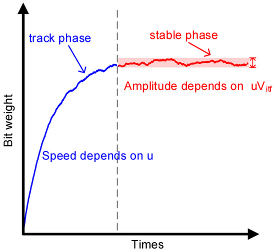
Figure 3.
Bit-weight learning curve.
In addition, since the real bit weight and the inter-stage gain change the same proportion compared to the ideal ones, the real inter-stage gain GR can be estimated as
where BW5I and BW5R represent the ideal and real bit weight of the 1st stage MSB, and GI is the ideal inter stage gain. BW5R is replaced by BW5(n) provided by the calibration, and they are only nearly equal in the LMS stable phase, which satisfies the requirement that only the Vtif needs to be eliminated during this phase. BW5I and GI are 211 and 23, hence (6) can be realized by 8-bit left shift of BW5R. Finally, the Vitf is estimated as
Subtracting Vtif from DBE can effectively suppress the signal interference and hence boost the calibration speed.
3. Simulation Results and Comparison
The proposed 12-bit pipeline-SAR ADC is simulated in MATLAB with 1V reference. The unit capacitor’s mismatch standard deviation of the first stage, sub-ADC 5 MSBs, second stage and sub-ADC 4 LSBs are 1%, 1%, 5% and 5%, respectively. Furthermore, the inter-stage gain is 7.2 with 20% error, compared with 8. In addition, of the offset between the sub-ADC and the main ADC is 5 mV, and the sampling capacitor of the first stage is 600 fF to add KT/C noise to signal.
To demonstrate the effectiveness of the proposed calibration algorithm, the full-scale sine wave input is simulated to observe the dynamic performance. One of the output spectra without and with calibration is shown in Figure 4. After calibration, SNDR and SFDR improve from 45.3 dB and 56.4 dB to 68.2 dB and 88.4 dB, respectively. Without and with signal elimination, simulations are executed with the same mismatch, and the dynamic performance learning curves are shown in Figure 5.
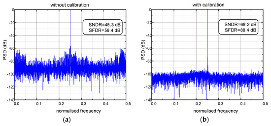
Figure 4.
Output spectra: (a) without calibration; (b) with calibration.
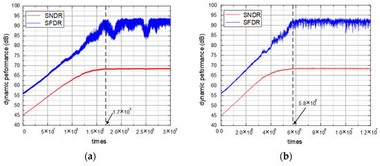
Figure 5.
ADC dynamic performance learning curves: (a) without signal elimination; (b) with signal elimination.
Although SNDR and SFDR are all over 67 dB and 80 dB after convergence, the convergence conversion cycles are 1.7 × 10⁸ and 5.8 × 10⁶ for without and with signal elimination. With DC, sine wave and the band-limited white noise input, the learning curves of bit weight BW5 are illustrated in Figure 6. Whatever the input is, BW5 can converge at about 6 × 10⁶ times and proves the signal independence.
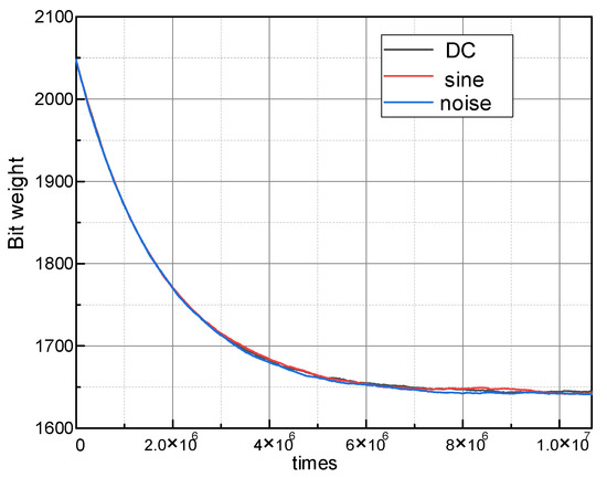
Figure 6.
MSB learning curve with DC, square and band-limited white noise inputs.
To evaluate the effect of the sub-ADC 5 MSBs’ capacitor mismatch to the signal cancellation, 400-time Monte Carlo simulations are performed with σ = 1% unit capacitor mismatch. The output spectra after convergence (5.8 × 10⁶ cycles) are statistically analyzed. Figure 7 shows the SFDR distribution histogram with the mean value E of 86.3 dB and standard variation σ of 1.1 dB, while SNDR is 68 dB and hardly changes, thus, it is not shown in Figure 7. The unit capacitor’s mismatch changes from 1% to 5%, and each case is simulated 1000 times. Figure 8 shows the worst case in 3σ principle, i.e., E−3σ, of SFDR. With 1% mismatch, SFDR is 83.0 dB, while it is 78.0 dB with 5% mismatch, which still maintains good calibration effect. A 5% mismatch is easily achieved in most processes, and, thus, the mismatch of the sub-ADC’s 5 MSBs does not limit the convergence acceleration.
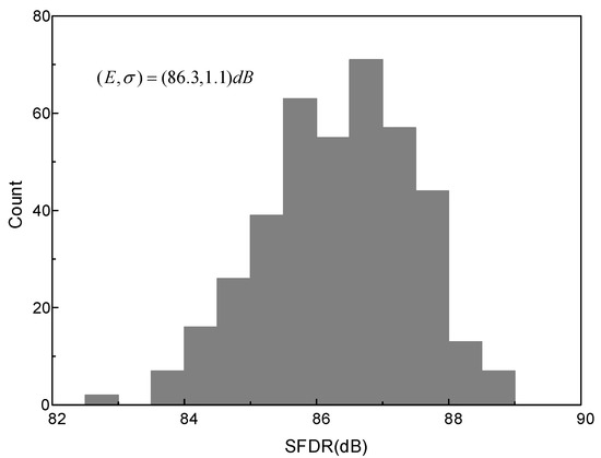
Figure 7.
Histogram of output spectra’s SFDR with mismatch of 1% of sub-ADC 5 MSBs.
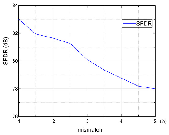
Figure 8.
SFDR with different mismatch of sub-ADC 5 MSBs.
As shown in Table 2, state-of-the-art background calibrations are listed. Compared to [11,12], this work and [13] are signal-independent. To achieve signal independence, ref. [13] requires complex shuffling and two-bit inter-stage redundancy, while, in this work, an auxiliary capacitor array with PN pre-injection technique realizes simple shuffling and occupies little residue headroom. The convergence cycles are less than [11], but more than [12,13]. Although the signal elimination in the proposed calibration can speed up convergence, there is mismatch between sub-ADC and main ADC, and this means that the signal cannot be estimated as accurately as in [12,13]. However, split-ADC and double second stage introduce more circuit hardware overhead.
Table 2.
Comparison with state-of-the-art calibrations.
4. Conclusions
In this brief, a signal-independent calibration with a convergence acceleration technique is developed. By introducing an auxiliary capacitor array to replace the DAC injected with PN to generate residue, and to reduce the residue range with the PN pre-injection technique, the signal independence is implemented. Furthermore, the signal interference is cancelled with the sub-ADC’s quantization result, and hence the convergence cycles decrease. The calibration is applied in a 12-bit pipeline-SAR ADC, which improves the SNDR and SFDR by 22.9 dB and 33.2 dB, respectively. Moreover, calibration converges in 5.8 × 10⁶ instead of 1.7 × 10⁸ cycles with signal elimination. In addition, the calibration operates normally no matter whether the input signal is DC, sine wave or band-limited white noise.
Author Contributions
Writing—original draft preparation, Y.-J.W.; writing—review and editing, P.W.; supervision, L.-X.W.; project administration, Z.J. All authors have read and agreed to the published version of the manuscript.
Funding
This research received no external funding.
Data Availability Statement
Not applicable.
Conflicts of Interest
The authors declare no conflict of interest.
References
- Liu, C.; Chang, S.; Huang, G.; Lin, Y. A 10-bit 50-MS/s SAR ADC With a Monotonic Capacitor Switching Procedure. IEEE J. Solid-State Circuits 2010, 45, 731–740. [Google Scholar] [CrossRef]
- Li, D.; Zhu, Z.; Ding, R.; Yang, Y. A 1.4-mW 10-Bit 150-MS/s SAR ADC With Nonbinary Split Capacitive DAC in 65-nm CMOS. IEEE Trans. Circuits Syst. II Express Briefs 2018, 65, 1524–1528. [Google Scholar] [CrossRef]
- Park, J.-S.; Jeon, J.-M.; Boo, J.-H.; Lee, J.-H.; Cho, K.-I.; Kim, H.-J.; Ahn, G.-C.; Lee, S.-H. A 2.2mW 12-bit 200MS/s 28nm CMOS Pipelined SAR ADC with Dynamic Register-Based High-Speed SAR Logic. In Proceedings of the 2020 IEEE Asian Solid-State Circuits Conference (A-SSCC), Hiroshima, Japan, 9–11 November 2020; pp. 1–2. [Google Scholar] [CrossRef]
- Liu, Q.; Shu, W.; Chang, J.S. A 1-GS/s 11-Bit SAR-Assisted Pipeline ADC With 59-dB SNDR in 65-nm CMOS. IEEE Trans. Circuits Syst. II Express Briefs 2018, 65, 1164–1168. [Google Scholar] [CrossRef]
- Lin, C.; Lee, T. A 12-bit 210-MS/s 2-Times Interleaved Pipelined-SAR ADC With a Passive Residue Transfer Technique. IEEE Trans. Circuits Syst. I Regul. Pap. 2016, 63, 929–938. [Google Scholar] [CrossRef]
- Lim, Y.; Flynn, M.P. 26.1 A 1mW 71.5dB SNDR 50MS/S 13b fully differential ring-amplifier-based SAR-assisted pipeline ADC. In Proceedings of the 2015 IEEE International Solid-State Circuits Conference—(ISSCC) Digest of Technical Papers, San Francisco, CA, USA, 22–26 February 2015; pp. 1–3. [Google Scholar] [CrossRef]
- Huang, H.; Sarkar, S.; Elies, B.; Chiu, Y. 28.4 A 12b 330MS/s pipelined-SAR ADC with PVT-stabilized dynamic amplifier achieving <1dB SNDR variation. In Proceedings of the 2017 IEEE International Solid-State Circuits Conference (ISSCC), San Francisco, CA, USA, 5–9 February 2017; pp. 472–473. [Google Scholar] [CrossRef]
- Verbruggen, B.; Deguchi, K.; Malki, B.; Craninckx, J. A 70 dB SNDR 200 MS/s 2.3 mW dynamic pipelined SAR ADC in 28nm digital CMOS. In Proceedings of the 2014 Symposium on VLSI Circuits Digest of Technical Papers, Honolulu, HI, USA, 10–13 June 2014; pp. 1–2. [Google Scholar] [CrossRef]
- Jiang, W.; Zhu, Y.; Zhang, M.; Chan, C.; Martins, R.P. 3.2 A 7.6mW 1GS/s 60dB SNDR Single-Channel SAR-Assisted Pipelined ADC with Temperature-Compensated Dynamic Gm-R-Based Amplifier. In Proceedings of the 2019 IEEE International Solid-State Circuits Conference—(ISSCC), San Francisco, CA, USA, 17–21 February 2019; pp. 60–62. [Google Scholar] [CrossRef]
- Zhou, Y.; Xu, B.; Chiu, Y. A 12 bit 160 MS/s Two-Step SAR ADC With Background Bit-Weight Calibration Using a Time-Domain Proximity Detector. IEEE J. Solid-State Circuits 2015, 50, 920–931. [Google Scholar] [CrossRef]
- Verbruggen, B.; Iriguchi, M.; de la Guia Solaz, M.; Glorieux, G.; Deguchi, K.; Malki, B.; Craninckx, J. A 2.1 mW 11b 410 MS/s dynamic pipelined SAR ADC with background calibration in 28nm digital CMOS. In Proceedings of the 2013 Symposium on VLSI Circuits, Kyoto, Japan, 12–14 June 2013; pp. C268–C269. [Google Scholar]
- Cao, Y.; Zhang, S.; Zhang, T.; Chen, Y.; Zhao, Y.; Chen, C.; Ye, F.; Ren, J. A 91.0-dB SFDR Single-Coarse Dual-Fine Pipelined-SAR ADC With Split-Based Background Calibration in 28-nm CMOS. IEEE Trans. Circuits Syst. I Regul. Pap. 2021, 68, 641–654. [Google Scholar] [CrossRef]
- Li, H.; Maddox, M.; Coin, M.C.W.; Buckley, W.; Hummerston, D.; Naeem, N. A signal-independent background-calibrating 20b 1MS/S SAR ADC with 0.3ppm INL. In Proceedings of the 2018 IEEE International Solid-State Circuits Conference—(ISSCC), San Francisco, CA, USA, 11–15 February 2018; pp. 242–244. [Google Scholar] [CrossRef]
- Lin, Y.; Liu, C.; Huang, G.; Shyu, Y.; Liu, Y.; Chang, S. A 9-Bit 150-MS/s Subrange ADC Based on SAR Architecture in 90-nm CMOS. IEEE Trans. Circuits Syst. I Regul. Pap. 2013, 60, 570–581. [Google Scholar] [CrossRef]
- Lim, Y.; Flynn, M.P. A calibration-free 2.3 mW 73.2 dB SNDR 15b 100 MS/s four-stage fully differential ring amplifier based SAR-assisted pipeline ADC. In Proceedings of the 2017 Symposium on VLSI Circuits, Kyoto, Japan, 5–8 June 2017; pp. C98–C99. [Google Scholar] [CrossRef]
Disclaimer/Publisher’s Note: The statements, opinions and data contained in all publications are solely those of the individual author(s) and contributor(s) and not of MDPI and/or the editor(s). MDPI and/or the editor(s) disclaim responsibility for any injury to people or property resulting from any ideas, methods, instructions or products referred to in the content. |
© 2023 by the authors. Licensee MDPI, Basel, Switzerland. This article is an open access article distributed under the terms and conditions of the Creative Commons Attribution (CC BY) license (https://creativecommons.org/licenses/by/4.0/).