

Investigation of Gallium Arsenide Deformation Anisotropy during Nanopolishing via Molecular Dynamics Simulation


Abstract
1. Introduction
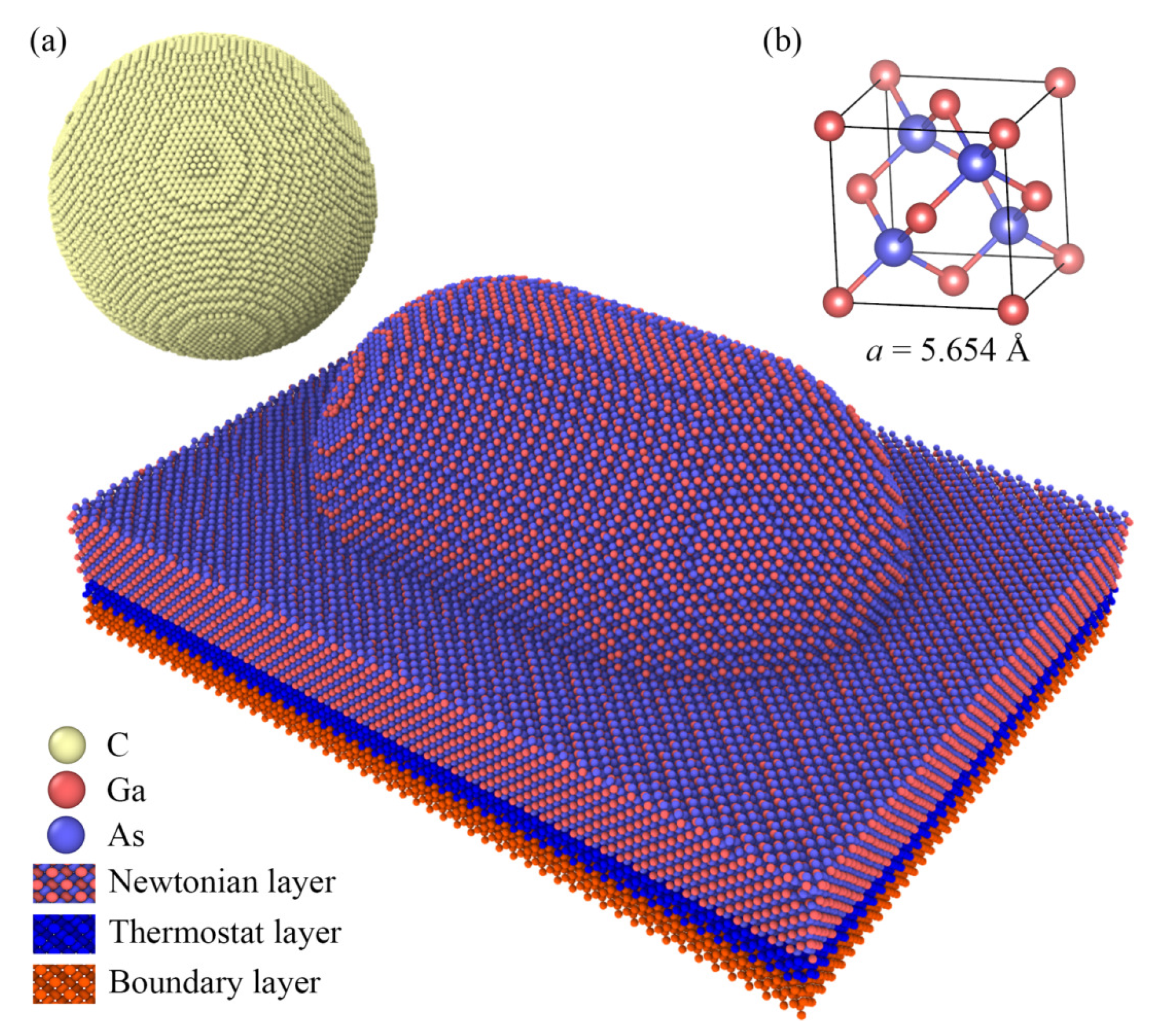
2. Methods
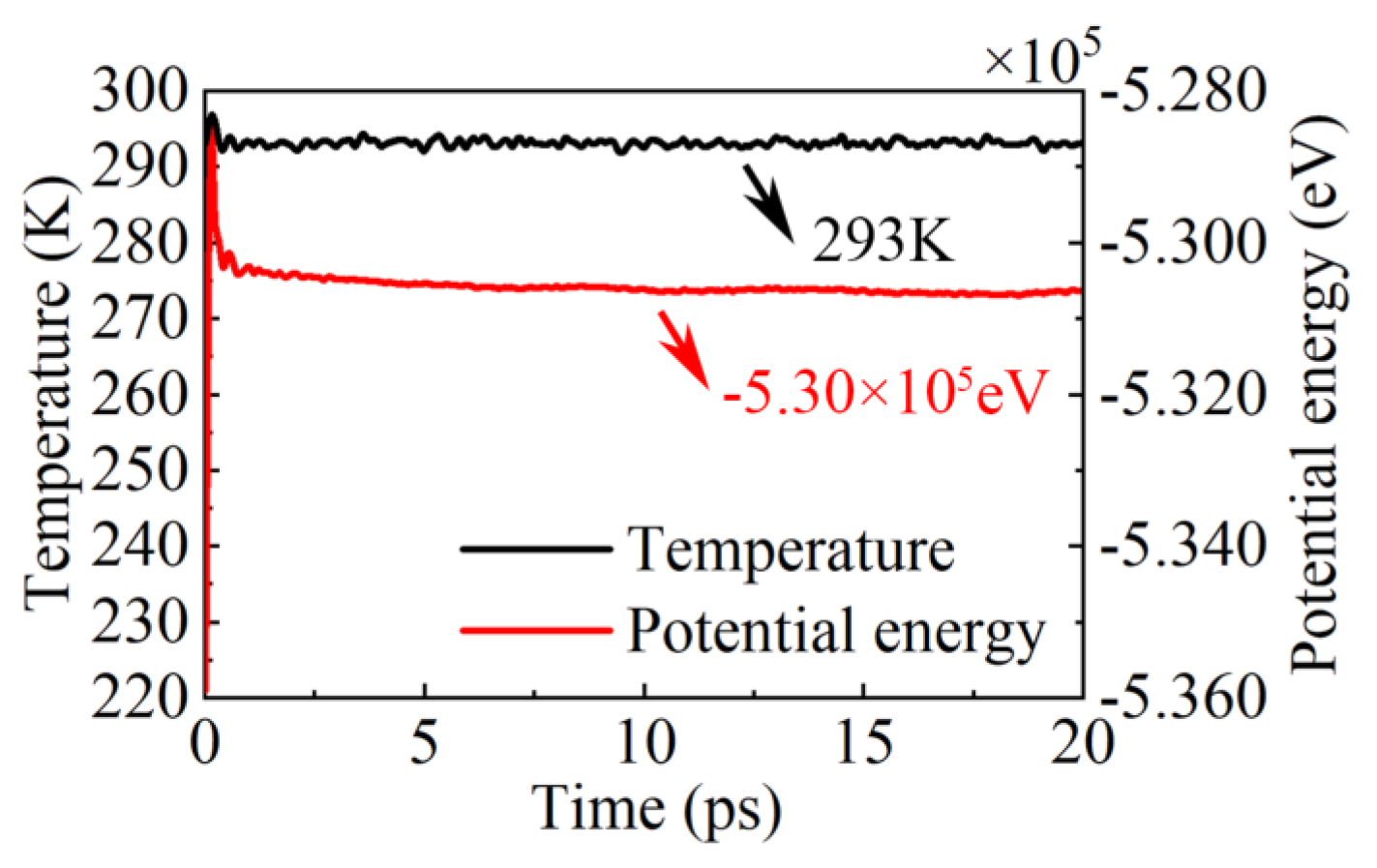
Simulation Methods
3. Results and Discussion
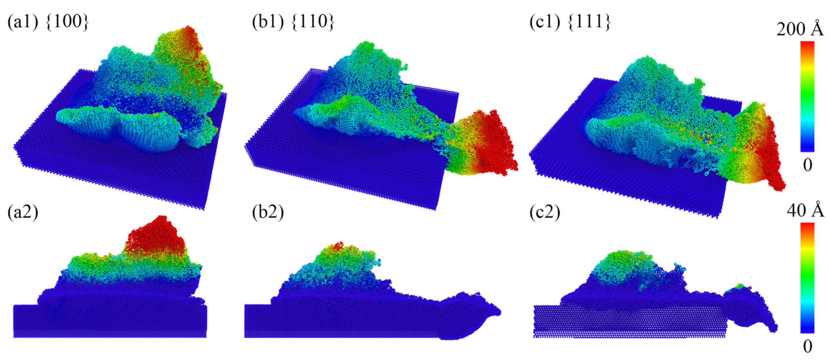
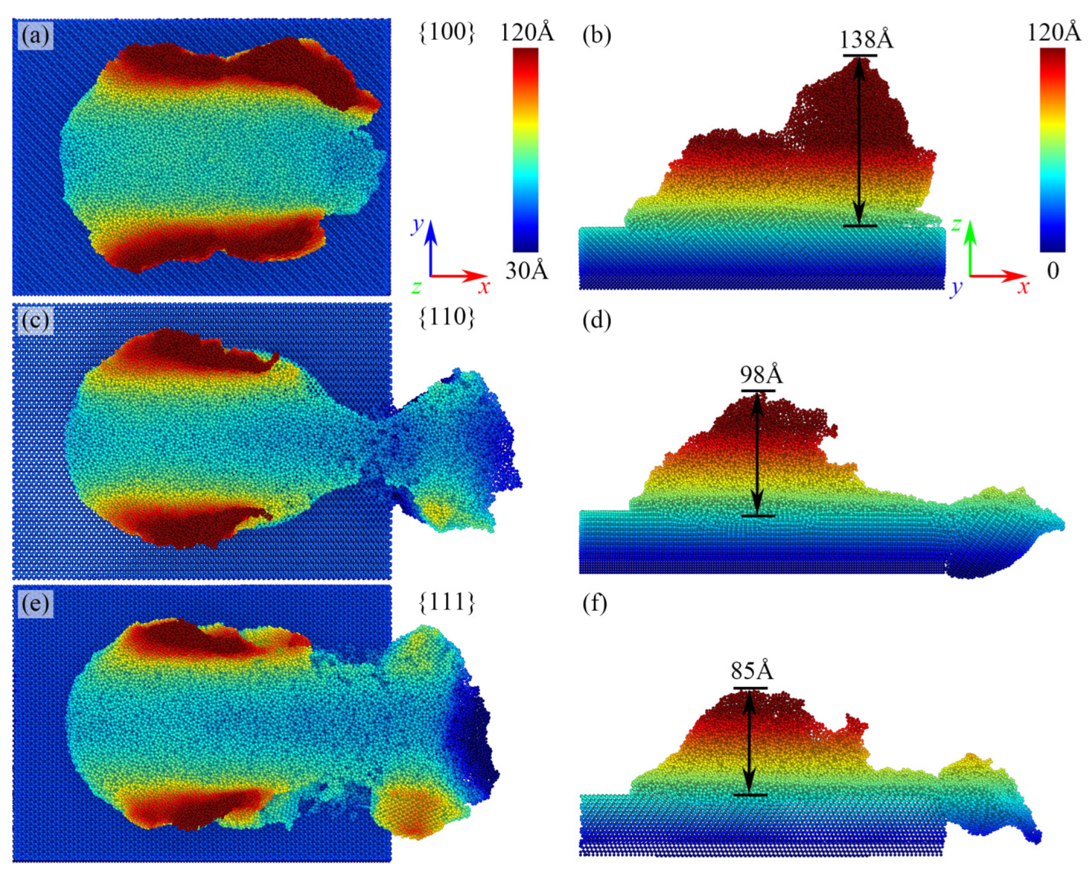
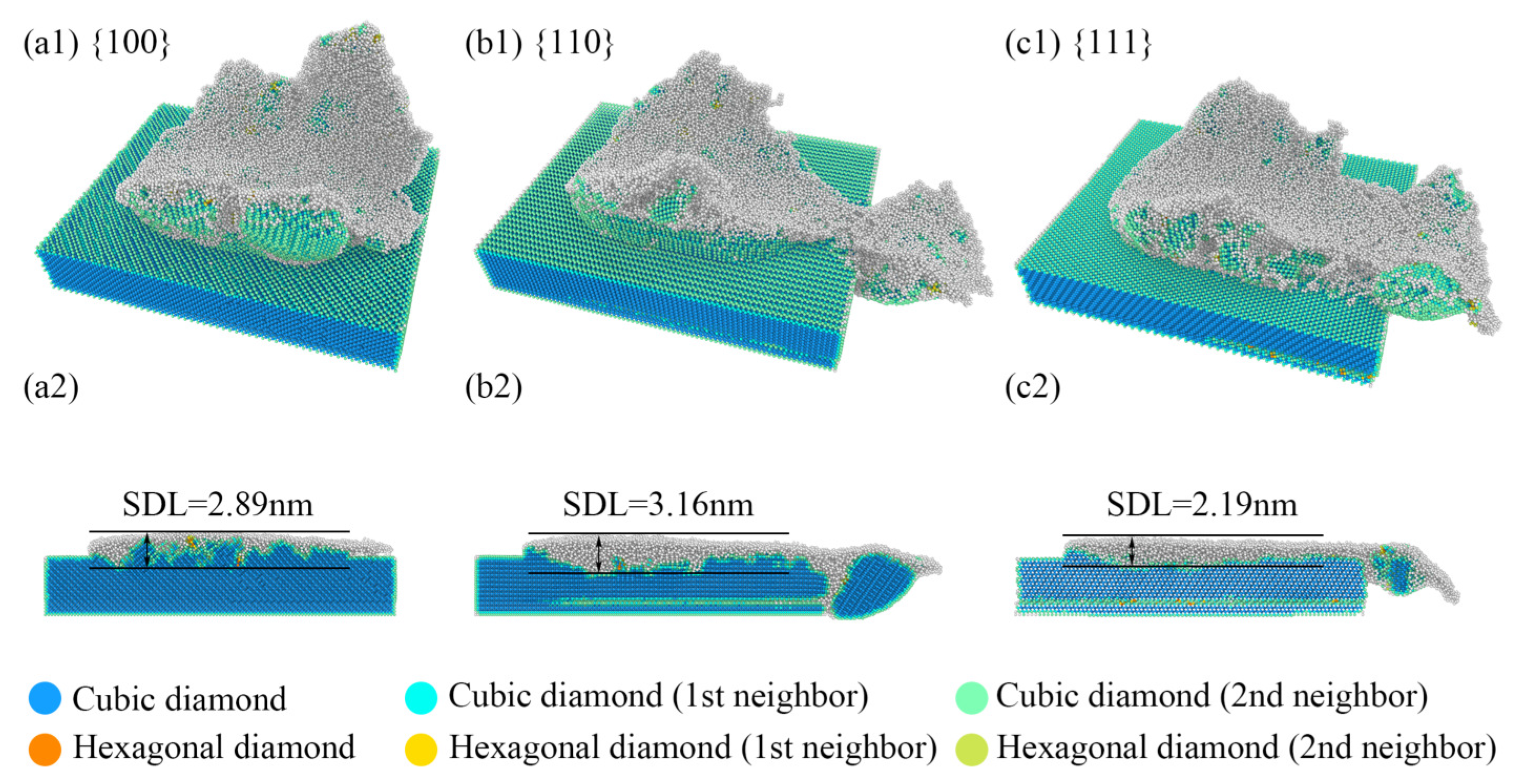
3.1. Surface Quality
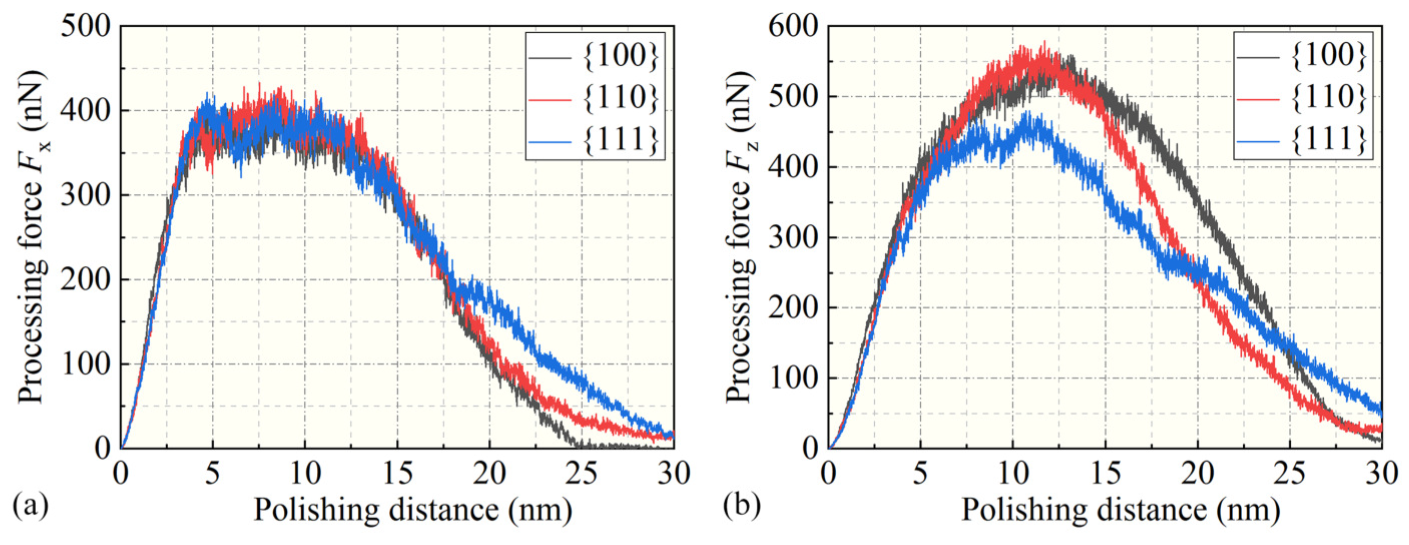
3.2. Mechanical Property
3.3. Amorphization Analysis
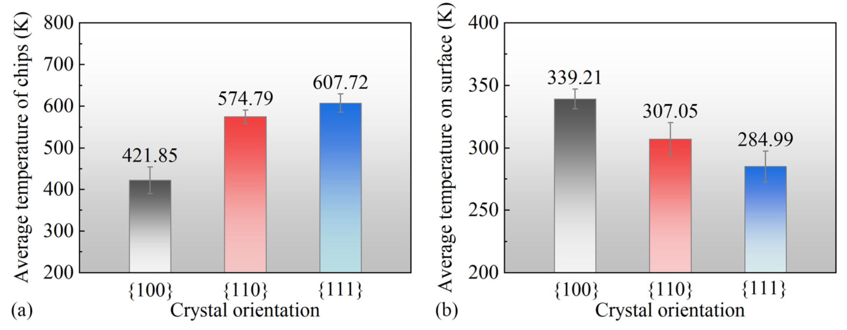
3.4. Analysis of Temperature Distribution
3.5. Analysis of Residual Stress
4. Conclusions
Author Contributions
Funding
Institutional Review Board Statement
Informed Consent Statement
Data Availability Statement
Acknowledgments
Conflicts of Interest
References
- Ahn, H.J.; Chang, W.I.; Kim, S.M.; Park, B.J.; Yook, J.M.; Eo, Y.S. 28 GHz GaAs pHEMT MMICs and RF front-end module for 5G communication systems. Microw. Opt. Technol. Lett. 2019, 61, 878–882. [Google Scholar] [CrossRef]
- Chow, T.P.; Omura, I.; Higashiwaki, M.; Kawarada, H.; Pala, V. Smart power devices and ICs using GaAs and wide and extreme bandgap semiconductors. IEEE Trans. Electron Devices 2017, 64, 856–873. [Google Scholar] [CrossRef]
- Hayati-Roodbari, N.; Wheeldon, A.; Hendler, C.; Fian, A.; Trattnig, R. Ohmic contact formation for inkjet-printed nanoparticle copper inks on highly doped GaAs. Nanotechnology 2021, 32, 225205. [Google Scholar] [CrossRef] [PubMed]
- Gao, J.; Zhou, H.; Du, J.; Peng, W.; Lin, Y.; Xiao, C.; Yu, B.; Qian, L. Effect of counter-surface chemical activity on mechanochemical removal of GaAs surface. Tribol. Int. 2022, 176, 107928. [Google Scholar] [CrossRef]
- Dinodiya, S.; Bhargava, A. A comparative analysis of pressure sensing parameters for two dimensional photonic crystal sensors based on Si and GaAs. Silicon 2022, 14, 4611–4618. [Google Scholar] [CrossRef]
- Hao, D.; Zhang, W.; Liu, X.; Liu, Y. A low insertion loss variation trombone true time delay in GaAs pHEMT monolithic microwave integrated circuit. IEEE Microw. Wirel. Components Lett. 2021, 31, 889–892. [Google Scholar] [CrossRef]
- Jordan, A.; Von Neida, A.; Caruso, R. The theoretical and experimental fundamentals of decreasing dislocations in melt grown GaAs and InP. J. Cryst. Growth 1986, 79, 243–262. [Google Scholar] [CrossRef]
- Xu, M.; Wu, Y.; Koybasi, O.; Shen, T.; Ye, P. Metal-oxide-semiconductor field-effect transistors on GaAs (111) A surface with atomic-layer-deposited Al2O3 as gate dielectrics. Appl. Phys. Lett. 2009, 94, 212104. [Google Scholar] [CrossRef]
- Bisson, S.; Kulp, T.; Levi, O.; Harris, J.; Fejer, M. Long-wave IR chemical sensing based on difference frequency generation in orientation-patterned GaAs. Appl. Phys. B 2006, 85, 199–206. [Google Scholar] [CrossRef]
- Johnson, K.L.; Johnson, K.L. Contact Mechanics; Cambridge University Press: Cambridge, UK, 1987. [Google Scholar]
- Hill, R. The Mathematical Theory of Plasticity; Oxford University Press: Oxford, UK, 1998; Volume 11. [Google Scholar]
- Gao, R.; Jiang, C.; Walker, D.; Li, H.; Zheng, Z. Molecular dynamics study on mechanical cleavage mechanisms of GaAs and experimental verification. Ceram. Int. 2022, 48, 36076–36083. [Google Scholar] [CrossRef]
- Li, Z.; Liu, L.; Wu, X.; He, L.; Xu, Y. Indentation induced amorphization in gallium arsenide. Mater. Sci. Eng. A 2002, 337, 21–24. [Google Scholar] [CrossRef]
- Li, Z.; Liu, L.; He, L.; Xu, Y.; Wu, X. Shear-activated indentation crack in GaAs single crystal. J. Mater. Res. 2001, 16, 2845–2849. [Google Scholar] [CrossRef]
- Wu, Y.; Huang, H.; Zou, J. Lattice bending in monocrystalline GaAs induced by nanoscratching. Mater. Lett. 2012, 80, 187–190. [Google Scholar] [CrossRef]
- Parlinska-Wojtan, M.; Wasmer, K.; Tharian, J.; Michler, J. Microstructural comparison of material damage in GaAs caused by Berkovich and wedge nanoindentation and nanoscratching. Scr. Mater. 2008, 59, 364–367. [Google Scholar] [CrossRef]
- Wasmer, K.; Parlinska-Wojtan, M.; Gassilloud, R.; Pouvreau, C.; Tharian, J.; Micher, J. Plastic deformation modes of gallium arsenide in nanoindentation and nanoscratching. Appl. Phys. Lett. 2007, 90, 03190. [Google Scholar] [CrossRef]
- Wasmer, K.; Parlinska-Wojtan, M.; Graça, S.; Michler, J. Sequence of deformation and cracking behaviours of Gallium–Arsenide during nano-scratching. Mater. Chem. Phys. 2013, 138, 38–48. [Google Scholar] [CrossRef]
- Gao, R.; Jiang, C.; Lang, X.; Dong, K.; Li, F. Experimental investigation of influence of scratch features on GaAs cleavage plane during cleavage processing using a scratching capability index. Int. J. Precis. Eng. Manuf.-Green Technol. 2021, 8, 761–770. [Google Scholar] [CrossRef]
- Yu, B.; Gao, J.; Chen, L.; Qian, L. Effect of sliding velocity on tribochemical removal of gallium arsenide surface. Wear 2015, 330, 59–63. [Google Scholar] [CrossRef]
- Chen, J.; Liang, Y.; Chen, M.; Bai, Q.; Tang, Y. A study of the subsurface damaged layers in nanoscratching. Int. J. Abras. Technol. 2009, 2, 368–381. [Google Scholar] [CrossRef]
- Fan, P.; Katiyar, N.K.; Goel, S.; He, Y.; Geng, Y.; Yan, Y.; Mao, H.; Luo, X. Oblique nanomachining of gallium arsenide explained using AFM experiments and MD simulations. J. Manuf. Process. 2023, 90, 125–138. [Google Scholar] [CrossRef]
- Gao, R.; Jiang, C.; Lang, X.; Zheng, Z.; Jiang, J.; Huang, P. Study on mechanical cleavage mechanism of GaAs via anisotropic stress field and experiments. IEEE Trans. Semicond. Manuf. 2022, 35, 633–640. [Google Scholar] [CrossRef]
- Wang, J.; Yan, Y.; Jia, B.; Geng, Y. Study on the processing outcomes of the atomic force microscopy tip-based nanoscratching on GaAs. J. Manuf. Process. 2021, 70, 238–247. [Google Scholar] [CrossRef]
- Wu, L.; Yu, B.; Fan, Z.; Zhang, P.; Feng, C.; Chen, P.; Ji, J.; Qian, L. Effects of normal load and etching time on current evolution of scratched GaAs surface during selective etching. Mater. Sci. Semicond. Process. 2020, 105, 104744. [Google Scholar] [CrossRef]
- Fang, T.H.; Chang, W.J.; Lin, C.M. Nanoindentation and nanoscratch characteristics of Si and GaAs. Microelectron. Eng. 2005, 77, 389–398. [Google Scholar] [CrossRef]
- Xuan, T.; Li, J.; Li, B.; Fan, W. Effects of the non-uniform magnetic field on the shear stress and the microstructure of magnetorheological fluid. J. Magn. Magn. Mater. 2021, 535, 168066. [Google Scholar] [CrossRef]
- Mahmood, A.; Chen, S.; Chen, C.; Weng, D.; Wang, J. Molecular dynamics study of temperature influence on directional motion of gold nanoparticle on nanocone surface. J. Phys. Chem. C 2019, 123, 4574–4581. [Google Scholar] [CrossRef]
- Li, B. Molecular Dynamics Simulations of Deformation Behavior of AlN in Nanoscratching. In Proceedings of the International Manufacturing Science and Engineering Conference, Online, 3 September 2020; American Society of Mechanical Engineers: New York, NY, USA, 2020; Volume 84256, p. V001T05A002. [Google Scholar]
- Yin, Z.; Zhu, P.; Li, B.; Xu, Y.; Li, R. Atomic simulations of deformation mechanism of 3C-SiC polishing process with a rolling abrasive. Tribol. Lett. 2021, 69, 146. [Google Scholar] [CrossRef]
- Chen, W.; Wang, W.; Liang, H.; Zhu, P. Molecular dynamics simulations of lubricant outflow in porous polyimide retainers of bearings. Langmuir 2021, 37, 9162–9169. [Google Scholar] [CrossRef]
- Li, B.; Li, J.; Xu, J.; Xuan, T.; Fan, W. Effects of cracking on the deformation anisotropy of GaAs with different crystal orientations during scratching using molecular dynamics simulations. Tribol. Int. 2023, 179, 108200. [Google Scholar] [CrossRef]
- Xu, X.; Fan, W.; Li, B.; Cao, J. Influence of GaAs crystal anisotropy on deformation behavior and residual stress distribution of nanoscratching. Appl. Phys. A 2021, 127, 690. [Google Scholar] [CrossRef]
- Yi, D.; Li, J.; Zhu, P. Study of nanoscratching process of GaAs using molecular dynamics. Crystals 2018, 8, 321. [Google Scholar] [CrossRef]
- Chen, C.; Lai, M.; Fang, F. Subsurface deformation mechanism in nano-cutting of gallium arsenide using molecular dynamics simulation. Nanoscale Res. Lett. 2021, 16, 117. [Google Scholar] [CrossRef] [PubMed]
- Li, B.; Li, J.; Fan, W.; Xuan, T.; Xu, J. The dislocation-and cracking-mediated deformation of single asperity GaAs during plowing using molecular dynamics simulation. Micromachines 2022, 13, 502. [Google Scholar] [CrossRef] [PubMed]
- Fan, P.; Goel, S.; Luo, X.; Yan, Y.; Geng, Y.; He, Y.; Wang, Y. Molecular dynamics simulation of AFM tip-based hot scratching of nanocrystalline GaAs. Mater. Sci. Semicond. Process. 2021, 130, 105832. [Google Scholar] [CrossRef]
- Fan, P.; Goel, S.; Luo, X.; Upadhyaya, H.M. Atomic-scale friction studies on single-crystal gallium arsenide using atomic force microscope and molecular dynamics simulation. Nanomanuf. Metrol. 2021, 5, 39–49. [Google Scholar] [CrossRef]
- Fan, P.; Goel, S.; Luo, X.; Yan, Y.; Geng, Y.; Wang, Y. An atomistic investigation on the wear of diamond during atomic force microscope tip-based nanomachining of gallium arsenide. Comput. Mater. Sci. 2021, 187, 110115. [Google Scholar] [CrossRef]
- Chen, C.; Lai, M.; Fang, F. Study on the crack formation mechanism in nano-cutting of gallium arsenide. Appl. Surf. Sci. 2021, 540, 148322. [Google Scholar] [CrossRef]
- Li, Z.; Yan, Y.; Wang, J.; Geng, Y. Molecular dynamics study on tip-based nanomachining: A review. Nanoscale Res. Lett. 2020, 15, 201. [Google Scholar] [CrossRef]
- Fan, P.; Goel, S.; Luo, X.; Yan, Y.; Geng, Y.; He, Y. Origins of ductile plasticity in a polycrystalline gallium arsenide during scratching: MD simulation study. Appl. Surf. Sci. 2021, 552, 149489. [Google Scholar] [CrossRef]
- Rino, J.P.; Chatterjee, A.; Ebbsjö, I.; Kalia, R.K.; Nakano, A.; Shimojo, F.; Vashishta, P. Pressure-induced structural transformation in GaAs: A molecular-dynamics study. Phys. Rev. B 2002, 65, 195206. [Google Scholar] [CrossRef]
- Kodiyalam, S.; Kalia, R.K.; Kikuchi, H.; Nakano, A.; Shimojo, F.; Vashishta, P. Grain boundaries in gallium arsenide nanocrystals under pressure: A parallel molecular-dynamics study. Phys. Rev. Lett. 2001, 86, 55. [Google Scholar] [CrossRef] [PubMed]
- Prasolov, N.; Brunkov, P.; Gutkin, A. Molecular dynamics simulations of GaAs-crystal surface modifications during nanoindentation with AFM tip. J. Phys. Conf. Ser. 2017, 917, 092018. [Google Scholar] [CrossRef]
- Güler, E.; Güler, M. Phase transition and elasticity of gallium arsenide under pressure. Mater. Res. 2014, 17, 1268–1272. [Google Scholar] [CrossRef]
- Spreiter, Q.; Walter, M. Classical molecular dynamics simulation with the Velocity Verlet algorithm at strong external magnetic fields. J. Comput. Phys. 1999, 152, 102–119. [Google Scholar] [CrossRef]
- Berendsen, H.J.; Postma, J.P.M.; van Gunsteren, W.F.; DiNola, A.; Haak, J.R. Molecular dynamics with coupling to an external bath. J. Chem. Phys. 1984, 81, 3684–3690. [Google Scholar] [CrossRef]
- Van Gunsteren, W.; Berendsen, H.J. Algorithms for macromolecular dynamics and constraint dynamics. Mol. Phys. 1977, 34, 1311–1327. [Google Scholar] [CrossRef]
- Stukowski, A. Visualization and analysis of atomistic simulation data with OVITO–the Open Visualization Tool. Model. Simul. Mater. Sci. Eng. 2009, 18, 015012. [Google Scholar] [CrossRef]
- Štich, I.; Car, R.; Parrinello, M.; Baroni, S. Conjugate gradient minimization of the energy functional: A new method for electronic structure calculation. Phys. Rev. B 1989, 39, 4997. [Google Scholar] [CrossRef]
- Erhart, P.; Albe, K. Analytical potential for atomistic simulations of silicon, carbon, and silicon carbide. Phys. Rev. B 2005, 71, 035211. [Google Scholar] [CrossRef]
- Albe, K.; Nordlund, K.; Nord, J.; Kuronen, A. Modeling of compound semiconductors: Analytical bond-order potential for Ga, As, and GaAs. Phys. Rev. B 2002, 66, 035205. [Google Scholar] [CrossRef]
- Ziegler, J.; Biersack, J.; Littmark, U. The Stopping and Range of Ions in Solids; Pergamon Press: New York, NY, USA, 1985. [Google Scholar]


| Simulation Parameters | Value |
|---|---|
| Material of the workpiece | Gallium arsenide (GaAs) |
| Material of the nanopolishing grit | Diamond (C) |
| Dimension of the workpiece (nm) | |
| Radius of the nanopolishing grit (nm) | 6 |
| Surface crystal orientation of the workpiece | , , and |
| Potential function | Tersoff, ZBL |
| Nanogrinding speed (m/s) | 100 |
| Ambient temperature (K) | 300 |
| Nanogrinding distance (nm) | 30 |
| Timestep (fs) | 1 |
Disclaimer/Publisher’s Note: The statements, opinions and data contained in all publications are solely those of the individual author(s) and contributor(s) and not of MDPI and/or the editor(s). MDPI and/or the editor(s) disclaim responsibility for any injury to people or property resulting from any ideas, methods, instructions or products referred to in the content. |
© 2024 by the authors. Licensee MDPI, Basel, Switzerland. This article is an open access article distributed under the terms and conditions of the Creative Commons Attribution (CC BY) license (https://creativecommons.org/licenses/by/4.0/).
Share and Cite
Zhao, B.; Gao, X.; Pan, J.; Liu, H.; Zhao, P. Investigation of Gallium Arsenide Deformation Anisotropy during Nanopolishing via Molecular Dynamics Simulation. Micromachines 2024, 15, 110. https://doi.org/10.3390/mi15010110
Zhao B, Gao X, Pan J, Liu H, Zhao P. Investigation of Gallium Arsenide Deformation Anisotropy during Nanopolishing via Molecular Dynamics Simulation. Micromachines. 2024; 15(1):110. https://doi.org/10.3390/mi15010110
Chicago/Turabian StyleZhao, Bo, Xifeng Gao, Jiansheng Pan, Huan Liu, and Pengyue Zhao. 2024. "Investigation of Gallium Arsenide Deformation Anisotropy during Nanopolishing via Molecular Dynamics Simulation" Micromachines 15, no. 1: 110. https://doi.org/10.3390/mi15010110
APA StyleZhao, B., Gao, X., Pan, J., Liu, H., & Zhao, P. (2024). Investigation of Gallium Arsenide Deformation Anisotropy during Nanopolishing via Molecular Dynamics Simulation. Micromachines, 15(1), 110. https://doi.org/10.3390/mi15010110