
Dielectric Engineering to Suppress Cell-to-Cell Programming Voltage Interference in 3D NAND Flash Memory


Abstract
:1. Introduction
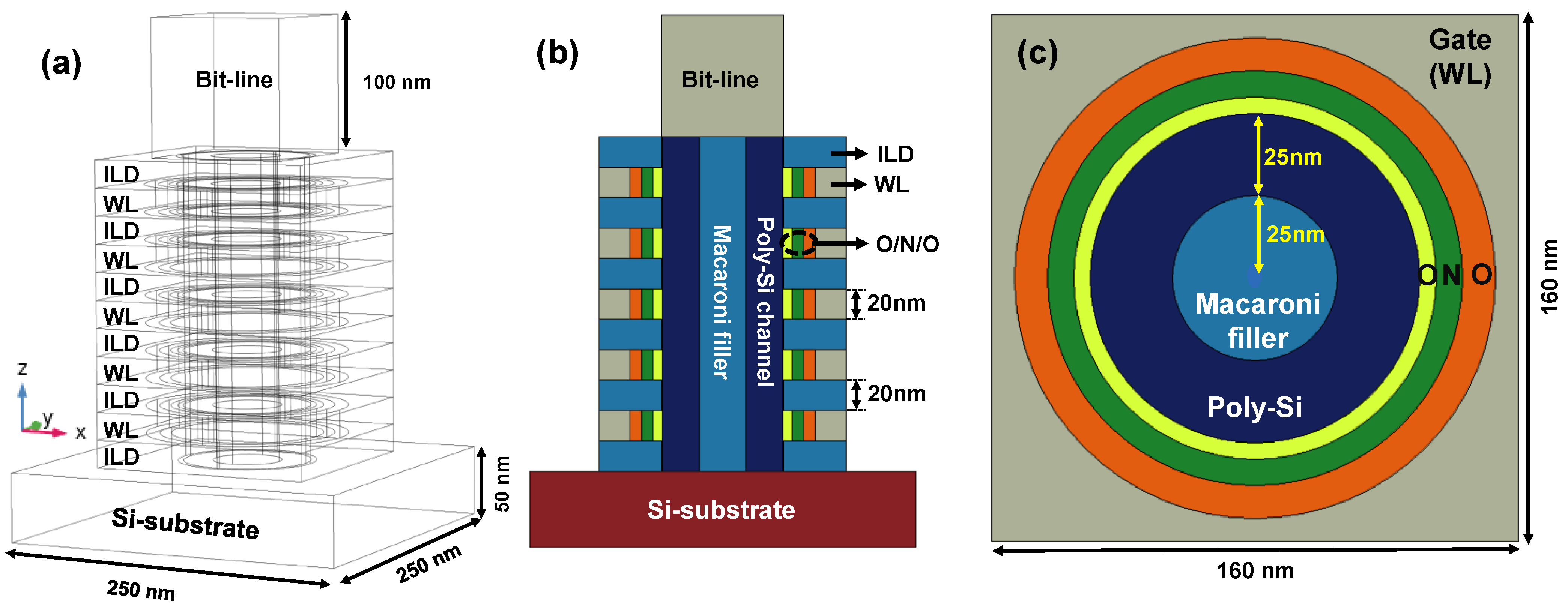
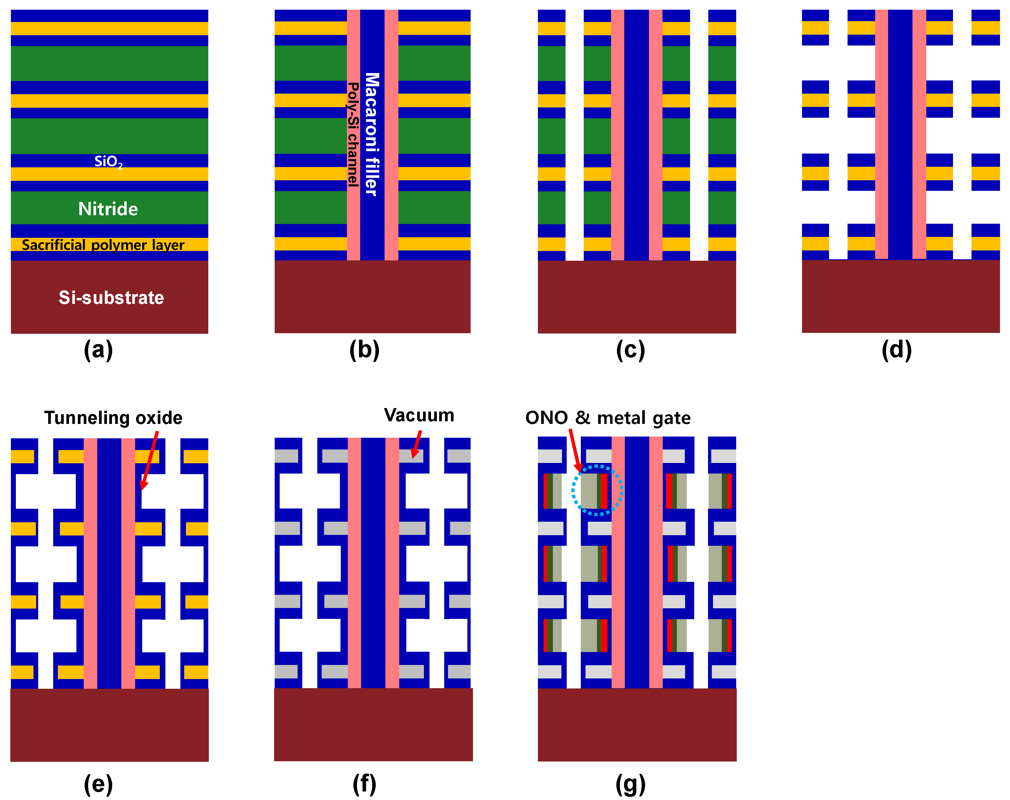
2. Materials and Methods
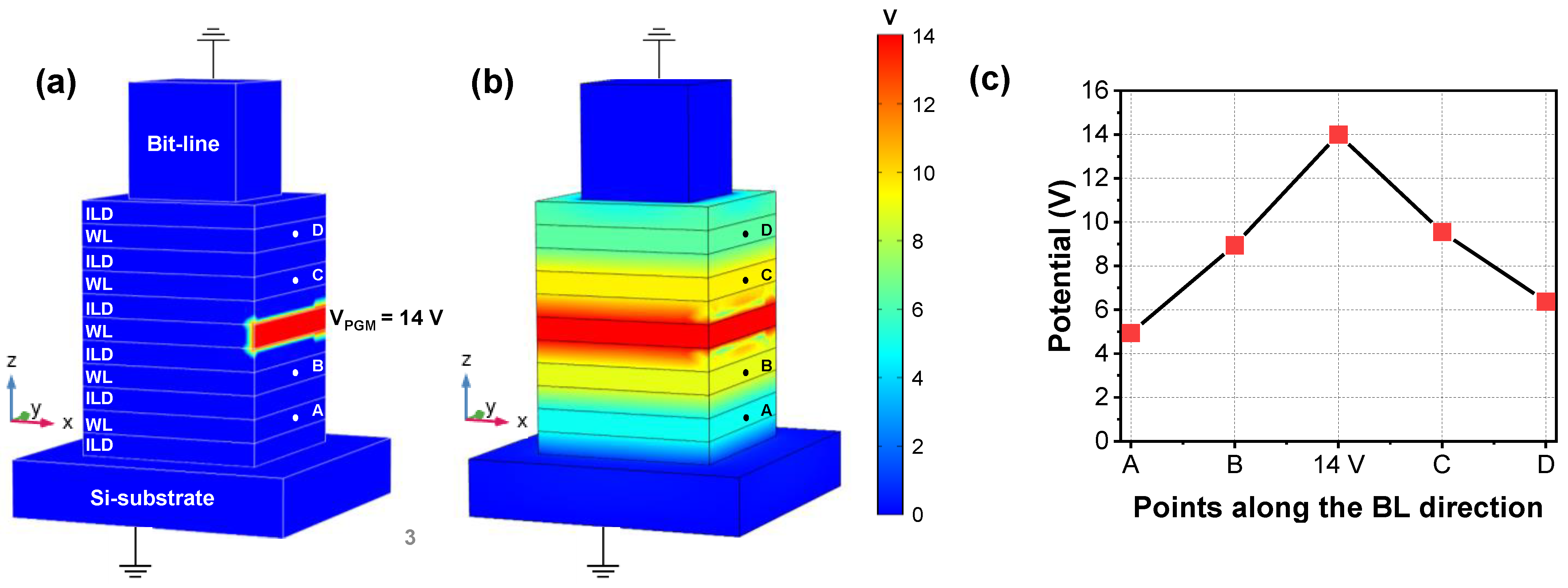
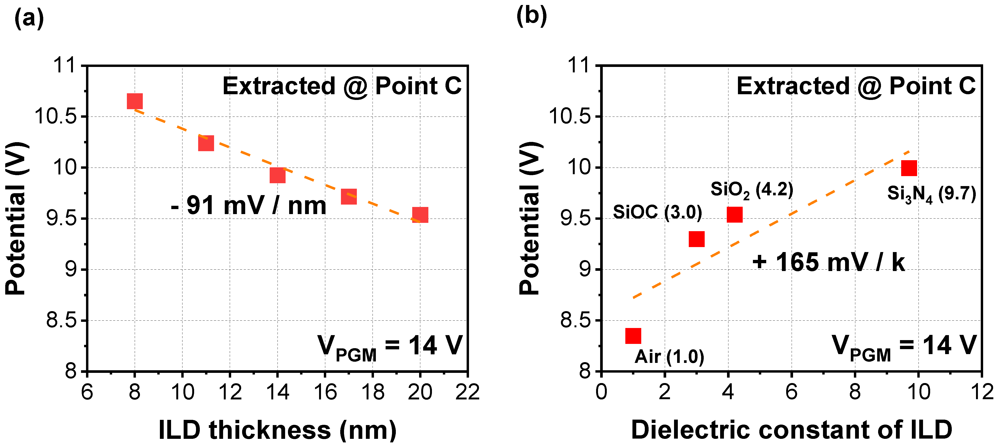
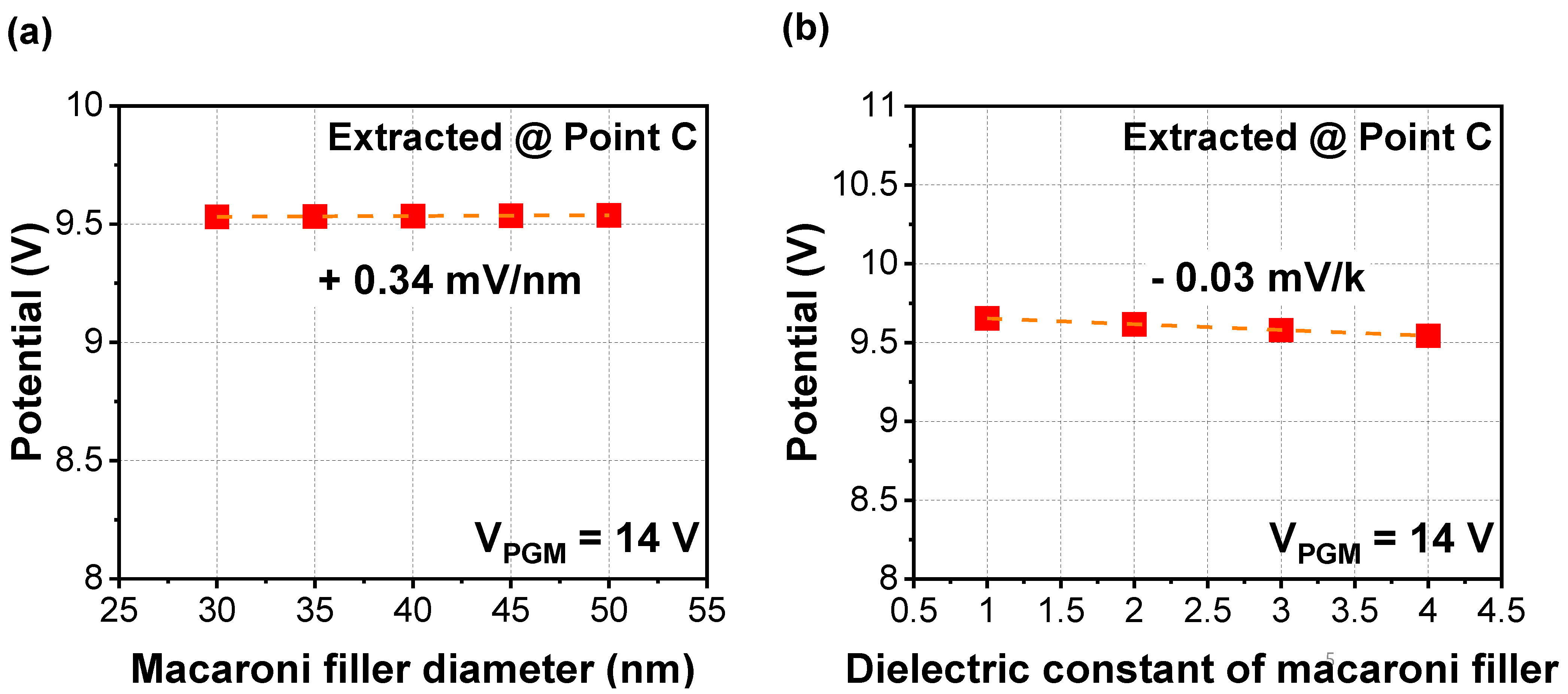
3. Results
4. Conclusions
Author Contributions
Funding
Institutional Review Board Statement
Informed Consent Statement
Acknowledgments
Conflicts of Interest
References
- Monzio Compagnoni, C.; Goda, A.; Spinelli, A.S.; Feeley, P.; Lacaita, A.L.; Visconti, A. Reviewing the Evolution of the NAND Flash Technology. Proceed. IEEE 2017, 105, 1609–1633. [Google Scholar] [CrossRef]
- Spinelli, A.S.; Malavena, G.; Lacaita, A.L.; Monzio Compagnoni, C. Random Telegraph Noise in 3D NAND Flash Memories. Micromachines 2021, 12, 703. [Google Scholar] [CrossRef] [PubMed]
- Yi, S.-I.; Kim, J. Novel Program Scheme of Vertical NAND Flash Memory for Reduction of Z-Interference. Micromachines 2021, 12, 584. [Google Scholar] [CrossRef] [PubMed]
- Lee, J.-D.; Hur, S.-H.; Choi, J.-D. Effects of floating-gate interference on NAND flash memory cell operation. IEEE Electron Device Lett. 2002, 23, 264–266. [Google Scholar] [CrossRef]
- Cai, Y.; Mutlu, O.; Haratsch, E.F.; Mai, K. Program interference in MLC NAND flash memory: Characterization, modeling, and mitigation. In Proceedings of the IEEE 31st International Conference on Computer Design (ICCD), Asheville, NC, USA, 6–9 October 2013; pp. 123–130. [Google Scholar] [CrossRef] [Green Version]
- Cai, Y.; Haratsch, E.F.; Mutlu, O.; Mai, K. Threshold voltage distribution in MLC NAND flash memory: Characterization, analysis, and modeling. In Proceedings of the 2013 Design, Automation & Test in Europe Conference & Exhibition (DATE), Grenoble, France, 18–22 March 2013; pp. 1285–1290. [Google Scholar] [CrossRef] [Green Version]
- Lue, H.-T.; Hsu, T.-H.; Wang, S.-Y.; Lai, E.-K.; Hsieh, K.-Y.; Liu, R.; Lu, C.-Y. Study of Incremental Step Pulse Programming (ISPP) and STI Edge Effect of BE-SONOS NAND Flash. In Proceedings of the 2008 IEEE International Reliability Physics Symposium, Phoenix, AZ, USA, 27 April–1 May 2008; pp. 693–694. [Google Scholar]
- Nguyen, T.; Duong Bang, D.; Wolff, A. 2019 Novel Coronavirus Disease (COVID-19): Paving the Road for Rapid Detection and Point-of-Care Diagnostics. Micromachines 2020, 11, 306. [Google Scholar] [CrossRef] [PubMed] [Green Version]
- COMSOL Multiphysics, version 5.4. In The AC/DC Module User’s Guide; COMSOL: Burlington, MA, USA, 2019; pp. 75–84.
- Jang, J.-H.; Kim, H.-S.; Cho, W.-S.; Cho, H.-S.; Kim, J.-H.; Shim, S.-I.; Jang, Y.-G.; Jeong, J.-H.; Son, B.-K.; Kim, D.-W.; et al. Vertical cell array using TCAT(Terabit Cell Array Transistor) technology for ultra high density NAND flash memory. In Proceedings of the 2009 Symposium on VLSI Technology, Kyoto, Japan, 15–17 June 2009; pp. 192–193. [Google Scholar]
- Kim, H.J.; Shao, Q.; Kim, Y.-H. Characterization of low-dielectric-constant SiOC thin films deposited by PECVD for interlayer dielectrics of multilevel interconnection. Surf. Coat. Technol. 2003, 171, 1–3. [Google Scholar] [CrossRef]
- Shah, K.; Singh, J.; Zayegh, A. Modelling and analysis of fringing and metal thickness effects in MEMS parallel plate capacitors. Microelectron. Des. Technol. Packag. II 2006, 6035, 603511. [Google Scholar] [CrossRef]
- Pundir, Y.P.; Bischt, A.; Saha, R.; Pal, P.K. Air-spacers as analog-performance booster for 5 nm-node N-channel nanosheet transistor. Semicond. Sci. Technol. 2021, 36, 9. [Google Scholar] [CrossRef]
- Sachid, A.B.; Huang, Y.-M.; Chen, Y.-J.; Chen, C.-C.; Lu, D.D.; Chen, M.-C.; Hu, C. FinFET With Encased Air-Gap Spacers for High-Performance and Low-Energy Circuits. IEEE Electron Device Lett. 2017, 38, 16–19. [Google Scholar] [CrossRef]
- Togo, M.; Tanabe, A.; Furukawa, A.; Tokunaga, K.; Hashimoto, T. A gate-side air-gap structure (GAS) to reduce the parasitic capacitance in MOSFETs. In Proceedings of the 1996 Symposium on VLSI Technology. Digest of Technical Papers, Honolulu, HI, USA, 11–13 June 1996; pp. 38–39. [Google Scholar] [CrossRef]
- Cheng, K.; Park, C.; Yeung, C.; Nguyen, S.; Zhang, J.; Miao, X.; Wang, M.; Mehta, S.; Li, J.; Surisetty, C.; et al. Air spacer for 10 nm FinFET CMOS and beyond. In Proceedings of the 2016 IEEE International Electron Devices Meeting (IEDM), San Francisco, CA, USA, 3–7 December 2016; pp. 17.1.1–17.1.4. [Google Scholar] [CrossRef]
- Park, J.-M.; Hwang, Y.-S.; Kim, S.-W.; Han, S.-Y.; Park, J.-S.; Kim, J.; Seo, J.-W.; Kim, B.-S.; Shin, S.-H.; Cho, C.-H.; et al. 20 nm DRAM: A new beginning of another revolution. In Proceedings of the 2015 IEEE International Electron Devices Meeting (IEDM), Washington, DC, USA, 7–9 December 2015; p. 26. [Google Scholar] [CrossRef]
- Chan, K.; Gleason, K.-K. Air-gap fabrication using a sacrificial polymeric thin film synthesized via initiated chemical vapor deposition. J. Electrochem. Soc. 2006, 153, 4. [Google Scholar] [CrossRef]
- Park, S.-H.; Allen, S.A.B.; Kohl, P.A. Air-Gaps for High-Performance On-Chip Interconnect Part II: Modeling, Fabrication, and Characterization. J. Electron. Mater. 2008, 37, 1534–1546. [Google Scholar] [CrossRef] [Green Version]


| Geometry | Material | Thickness [nm] | Dielectric Constant | Electrical Conductivity [S/m] |
|---|---|---|---|---|
| Word-line (WL) | W | 20 | 1 | 2 × 10⁶ |
| Blocking oxide | Al₂O₃ | 10 | 5.7 | 10−11 |
| Charge trap layer | Si3N4 | 8 | 9.7 | 10−11 |
| Tunneling oxide | SiO2 | 5 | 4.2 | 10−11 |
| Poly-Si channel | Poly-Si | 25 | 4.5 | 3 × 10³ |
| Si-substrate | Si | 50 | 11.7 | 104 |
| Macaroni filler | SiO2 | 50 | 4.2 | 10−11 |
| Bit-line (BL) contact | W | 100 | 1 | 2 × 10⁶ |
| Inter-layer dielectric (ILD) | SiO2 | 20 | 4.2 | 10−11 |
| Geometry | Material | Thickness | Dielectric Constant |
|---|---|---|---|
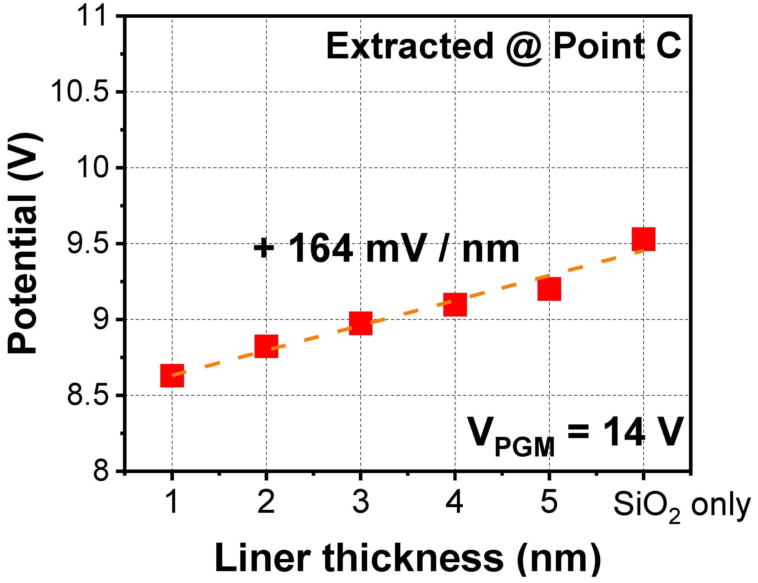
| Inter-layer dielectric (ILD) | SiO2 | −91 mV/nm | +165 mV/k |
| Macaroni filler | SiO2 | +0.34 mV/nm | −0.03 mV/k |
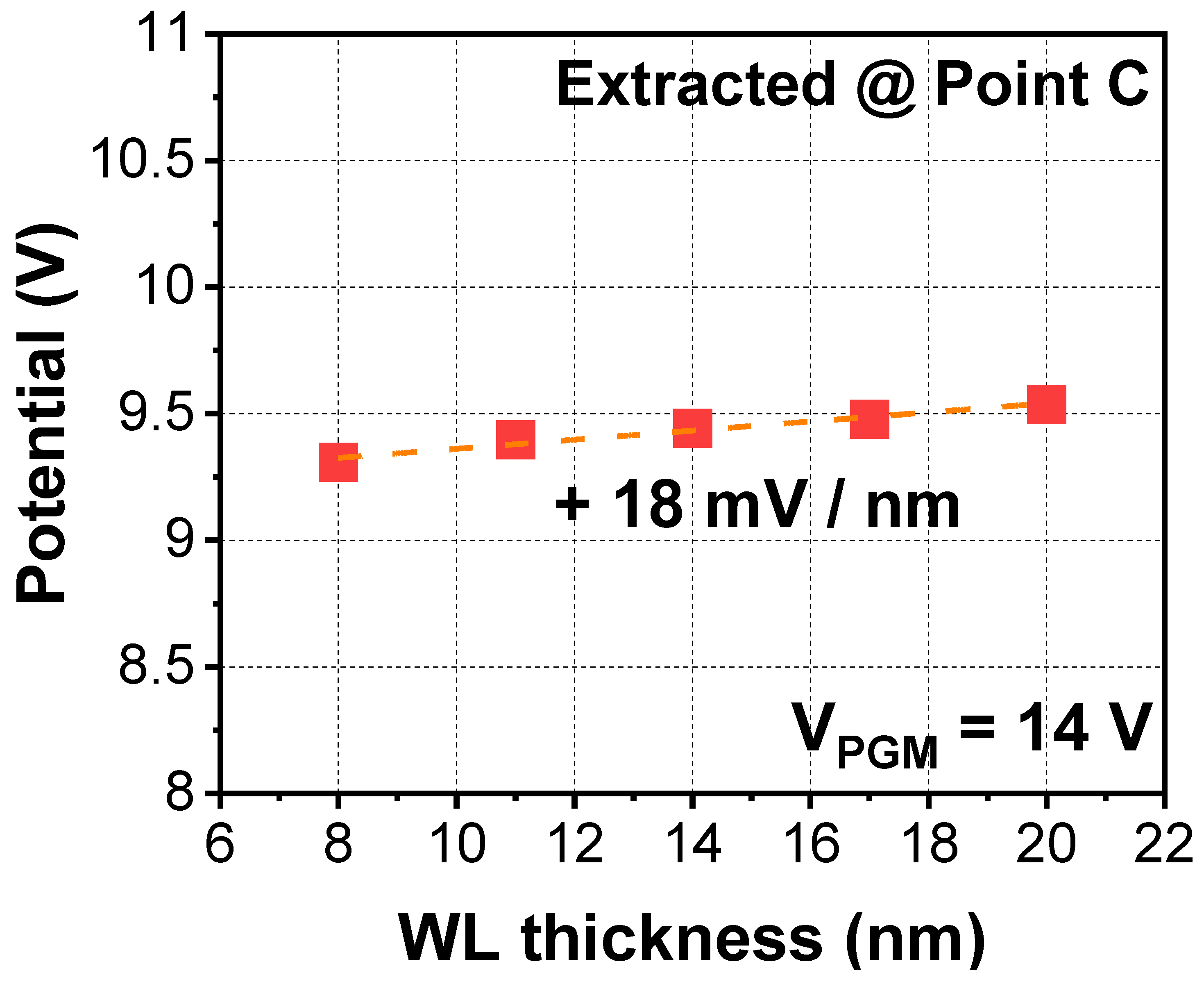
| Word-line (WL) | W | +18 mV/nm | - |
Publisher’s Note: MDPI stays neutral with regard to jurisdictional claims in published maps and institutional affiliations. |
© 2021 by the authors. Licensee MDPI, Basel, Switzerland. This article is an open access article distributed under the terms and conditions of the Creative Commons Attribution (CC BY) license (https://creativecommons.org/licenses/by/4.0/).
Share and Cite
Jung, W.-J.; Park, J.-Y. Dielectric Engineering to Suppress Cell-to-Cell Programming Voltage Interference in 3D NAND Flash Memory. Micromachines 2021, 12, 1297. https://doi.org/10.3390/mi12111297
Jung W-J, Park J-Y. Dielectric Engineering to Suppress Cell-to-Cell Programming Voltage Interference in 3D NAND Flash Memory. Micromachines. 2021; 12(11):1297. https://doi.org/10.3390/mi12111297
Chicago/Turabian StyleJung, Woo-Jin, and Jun-Young Park. 2021. "Dielectric Engineering to Suppress Cell-to-Cell Programming Voltage Interference in 3D NAND Flash Memory" Micromachines 12, no. 11: 1297. https://doi.org/10.3390/mi12111297
APA StyleJung, W.-J., & Park, J.-Y. (2021). Dielectric Engineering to Suppress Cell-to-Cell Programming Voltage Interference in 3D NAND Flash Memory. Micromachines, 12(11), 1297. https://doi.org/10.3390/mi12111297