Abstract
For the application of a digital array signal processing system with a high sampling rate and large bandwidth, and considering the constraints of limited resources (performance, volume, power consumption, weight, etc.), this paper proposes a design and implementation method of broadband digital array signal processing system based on radio frequency system on a chip. The system focuses on multi-channel synchronization under a high sampling rate and multi-channel amplitude and phase calibration under large bandwidth to form an all-digital, low-power, multi-channel, high-speed, large bandwidth hardware platform suitable for broadband digital array signal processing. Through the implementation of the Multiple-Input Multiple-Output phased-array digital beamforming algorithm, the test conducted verifies that the system has superior signal processing performance of the broadband digital array.
1. Introduction
With the development of radar technology and the increasingly complex combat environment, modern high-tech warfare has put forward increasingly higher requirements for radar systems. Broadband radar is valued by countries all over the world for its advantages, including high distance resolution, anti-jamming capability, and excellent target detection and identification abilities. Meanwhile, the introduction of digital technology in broadband radar systems makes it easy to realize transmit beamforming through time delay adjustment and provides great flexibility for resource scheduling. The broadband digital array radar combining broadband phased array and digital technology is an advanced and ideal radar system with urgent application demand and extensive application scenarios. As the core of broadband digital array radar, the broadband digital array signal processing system is particularly important.
In recent years, different architectures of digital array signal processing systems have been proposed by domestic and international research institutions [1,2,3,4,5,6,7,8]. In 2015, the Institute for Microwave and Radar Research of the German Aerospace Center proposed a satellite-integrated dual-frequency digital array signal processing system that uses a two-dimensional patch to achieve Digital Beam-Forming (DBF) [9]. This structure is not conducive to consistent multi-channel calibration, resulting in less flexibility. In 2019, Xidian University completed a digital array signal processing system based on the RF transceiver AD9371 that uses a zero Intermediate Frequency (IF) architecture to achieve DBF of 64 antenna units. However, it is limited by the sampling rate of the RF transceiver and thus cannot perform digital array signal processing with a large instantaneous bandwidth [10]. At present, there is a system scheme that uses two channels to generate large instantaneous bandwidth radar signals [11] that occupy more channels and makes it difficult to meet the application scenarios of multi-channel radar systems. There is also a design solution that uses the discrete device approach of high-speed Analog-to-Digital Converter (ADC) and Digital-to-Analog Converter (DAC) chips combined with Field Programmable Gate Arrays (FPGAs) [12]. Its system has a larger size and greater power consumption, and the ADC/DAC consumes a large amount of high-speed interface, which puts higher demands on the FPGA resources.
As the armed system is given higher index requirements, the performance requirement of the radar system is also higher. For the MIMO and phased array radar system, the number of channels and the volume also increase. Meanwhile, a large instantaneous bandwidth of the signal is required to improve the accuracy of a radar in the range and bearing dimensions and to classify and identify multiple targets. To address the above needs and embrace future development trends based on the on-chip RF integrated system chip (RFSoC), this paper adopts the high intermediate frequency (HIF) architecture and combines multi-channel synchronization with calibration techniques under a high sampling rate and a large bandwidth to design an all-digital, low-power, multi-channel, high-speed broadband digital array signal processing system with 64 receive channels and 64 transmit channels in a small volume to form a hardware platform for multi-channel radar system application and meet the application requirements of high performance and small volume.
2. System Architectural Design
Existing array radar signal processing systems are usually composed of discrete ADCs/DACs and multi-stage microwave frequency conversion components. When the radar system has more transceiver channels, it often requires a larger size, weight, and power consumption, which are often difficult to satisfy in resource-constrained application scenarios such as spaceborne, airborne, and missile-borne. At the same time, when the radar signal is broadband, it puts a high demand on the sampling rate and bandwidth of the system.
This section describes an RFSoC-based broadband digital array signal processing system architecture design, focusing on hardware architecture and software architecture. The system operates over a wide band coverage, which is very suitable for broadband digital array signal processing, particularly for L, S, and C band system applications. In addition, the system has great technical advantages and application prospects in resource-constrained (size, performance, and power consumption) application scenarios.
2.1. System Hardware Architecture Design
2.1.1. Overall Framework Design
The hardware architecture of the broadband digital array signal processing system consists of three main parts: the digital array signal processor, the RF front-end, and the antenna array. The hardware architecture is shown in Figure 1.
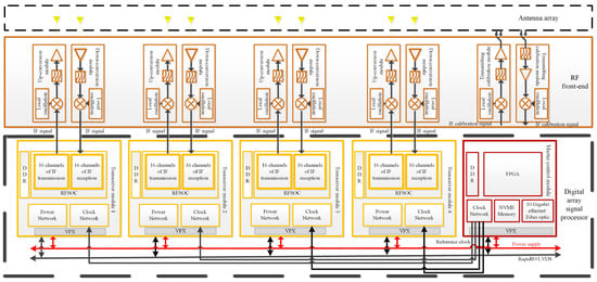
Figure 1.
System hardware architecture.
The digital array signal processor is mainly responsible for transmitting and receiving IF signals and interacting with the outside world for commands and data. It is designed with the 6U VPX standard structure consisting of four transceiver modules and one master control module; the different modules are interconnected by high-speed serial buses. The transceiver module realizes the processing of baseband signals and the transmission and reception of HIF signals. The main control module realizes external communication, reports the system working status, data processing results, etc., through the 10 Gigabit Ethernet and optical fiber. It also performs task configuration for each module in the processor, coordinates the workflow of the whole processor, and generates specific radar working timing signals.
The RF front end is responsible for the reception and transmission of RF signals, which consists of an up-conversion module, a down-conversion module, and a calibration module. The frequency conversion module realizes the conversion of the IF signal and RF signal, and the calibration module realizes the online amplitude and phase calibration of multiple transceiver channels.
2.1.2. Hardware Design of the Transceiver Module
The hardware architecture of the transceiver module, which integrates 2 RFSoC chips with 16 transmit channels and 16 receive channels, is shown in Figure 2.
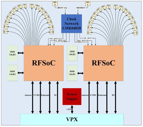
Figure 2.
Hardware architecture of transceiver module.
The RFSoC is an on-chip RF system developed by XILINX using 16 nm technology [13]. It integrates high-performance ADCs and DACs in the SoC, replaces discrete data converters with integrated direct RF sampling technology, and integrates high-speed data links on-chip, enabling a 50–75% reduction in power consumption and package size. Its 10 GSPS sampling rate DAC and 5 GSPS sampling rate ADC can realize broadband signal acquisition and transmission, and its 0–6 GHz wide analog bandwidth, on-chip digital up converter (DUC), and on-chip digital down converter (DDC) can realize direct RF input/output or HIF input/output [14]. Each RFSoC is connected to two DDR memory chips that can realize fast caching of large-capacity data. To achieve high-speed synchronization between the chips, the transceiver module uses a low-skew and low-jitter LMK04828 clock network to simultaneously provide clocks for both RFSoCs, providing clock synchronization as the hardware basis for the synchronization work between the channels of the whole system.
The actual transceiver module is shown in Figure 3.
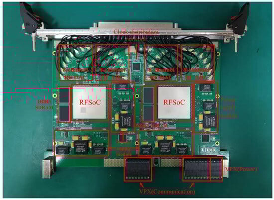
Figure 3.
Physical receiving and sending modules.
The two RFSoC circuits use the same PCB layout and wiring, and the external interface of the IF signal uses arc lines, which can better ensure multi-channel consistency and isolation.
The isolation between channels is simulated, and the isolations between ADC channels, DAC channels, ADC channels and clocks, and DAC channels and clocks are tested separately. The simulation results show that isolation between channels is better than −60 dB in the frequency range 0–10 GHz (Figure 4).
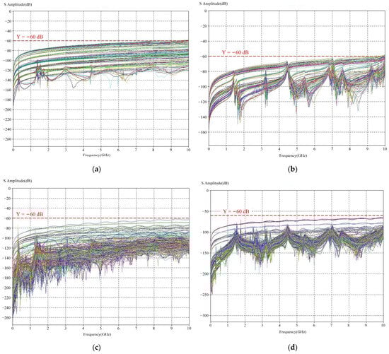
Figure 4.
Simulation of inter-channel isolations: (a) Simulation between ADC channels; (b) Simulation between DAC channels; (c) Simulation between ADC channels and clock; (d) Simulation between DAC channels and clock.
The results of simulating and testing amplitude and phase consistency between ADC and DAC channels, respectively, are shown in Figure 5. The simulation input/output signal is a single frequency signal at 3 GHz. It can be seen from Figure 5 that the amplitude consistency of each channel is less than ±0.3 V, and the time delay between channels is less than ±5 ps.
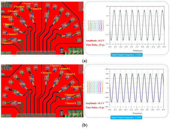
Figure 5.
Simulation of amplitude-phase consistency between channels: (a) Simulation between ADC channels; (b) Simulation between DAC channels.
2.1.3. Clock Network Design
To achieve synchronous sampling of multiple channels, the transceiver module uses a multi-chip LMK04828 synchronous clock network structure, as shown in Figure 6. This structure consists of a master LMK04828 chip and slave LMK04828 chips. LMK04828 is the master chip in the master control module and the slave chip in the transceiver module. The master chip provides the reference clock and synchronization clock for each slave chip to synchronize the output clock of each slave chip, and the slave chip provides the sampling reference clock and SYSREF for multiple RFSoCs.
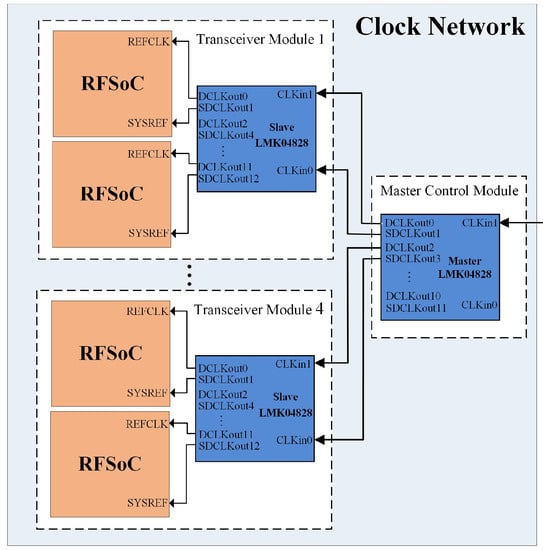
Figure 6.
System Clock Network.
To reduce the phase difference provided by the master chip to the slave chip clock, the clock path from the master chip to each slave chip should be strictly equal in length. At the same time, LMK04828 has a clock channel analog delay function that can independently control the output clock delay of each channel. Its minimum delay accuracy of up to 25 ps can make up for the physical delays of different clock paths.
2.1.4. Design of Digital HIF Architecture
In traditional array signal processing systems, the baseband signal processor generates a lower IF signal. When the operating band is high, a multi-stage RF up/down conversion to the RF band is required. This increases the size and power consumption of the RF front end.
The RFSoC enables a digital HIF architecture due to its ultra-wide analog bandwidth, from 0–6 GHz, and internal DUC and DDC, as shown in Figure 7. Meanwhile, compared with the traditional RF transceiver implementation of the HIF architecture [11], the digital HIF architecture can realize the numerically controlled oscillator (NCO) reset, which solves the problem of the traditional HIF architecture being unable to synchronize the phase of each channel’s local oscillation [15].
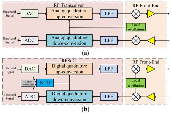
Figure 7.
HIF architecture: (a) Traditional analog HIF architecture; (b) Digital HIF architecture.
The digital quadrature up/down conversion can generate two perfectly quadrature local oscillation signals, and their local oscillation frequencies and phases can be precisely controlled. The frequency accuracy is calculated using Equation (1). In contrast, the analog quadrature up/down conversion used in the conventional architecture generates two quadrature local oscillation signals with certain phase deviation, which leads to an I/Q imbalance in the up/down conversion and generates a mirror frequency that is difficult to suppress [16].
2.2. System Software Architecture Design
The software architecture of the broadband digital array signal processing system is shown in Figure 8. The software process includes system control, data exchange, IF pre-processing, HIF architecture implementation, multi-channel synchronization, broadband calibration, and MIMO phased array digital multi-beam formation.
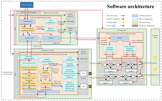
Figure 8.
System software architecture.
The main goal of system control and data interaction is to realize the transmission and storage of the original baseband signal data, the control of radar parameters such as beam pointing angle and PRT, the setting of RF front-end attenuation and inverter local oscillation frequency, and the configuration of clock network and sampling, etc.
IF pre-processing and HIF architecture implementation involve the processing of IF signals by the transceiver module before and after RF conversion, including DUC, DDC, extraction, interpolation, and other operations, to achieve HIF architecture.
Multi-channel synchronization means that the transceiver module realizes high-speed synchronous sampling of multiple transceiver channels in IF through the internal self-synchronization mechanism of RFSoC and the external clock network synchronization. Each channel can realize synchronous sampling under a sampling rate of up to 10 GSPS.
Broadband calibration means solving amplitude-phase errors caused by channel amplitude-phase inconsistencies in a wide band by constructing equalization filters.
MIMO phased array digital multibeam formation involves the implementation of the MIMO phased array digital multibeam formation algorithm in the system to verify the digital array signal processing capability.
2.2.1. Multi-Channel Synchronous Design
The design of multi-channel synchronization requires the synchronization of multiple RFSoC inter-chip transceiver channels on four transceiver modules. First, we synchronize the clock networks of each transceiver module so that the sampling reference clocks and SYSREF output from each clock network are synchronized. At the same time, under the premise of the sampling reference clock and SYSREF synchronization, RFSoC’s inter-chip synchronization mechanism is used to achieve ADC/DAC converter synchronization. After converter synchronization, if the system adopts the HIF architecture to enable the internal digital up/down converter, it is necessary to reset the digital up/down converter NCO local oscillation phase in each transceiver module to finally realize the inter-chip transceiver channel synchronization.
Compared with other acquisition/transmission systems, RFSoC uses its internal API function for synchronization. Through the internal synchronization mechanism and the system clock network, the synchronization process shown in Figure 9 is used to achieve multi-channel synchronization between multiple transceiver modules of the system.
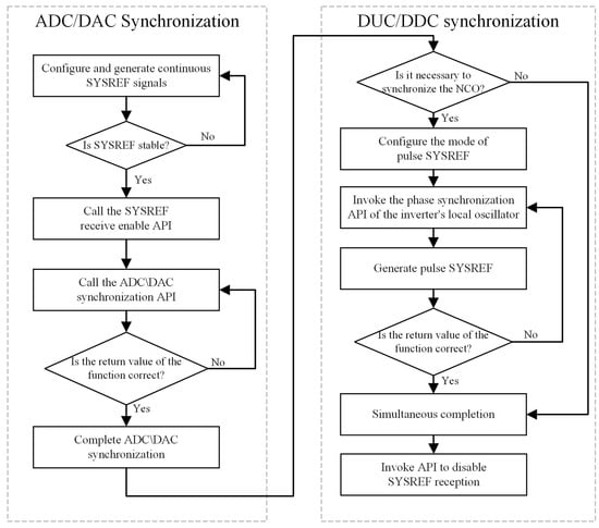
Figure 9.
Synchronization processes.
After multi-channel synchronization between multiple transceiver modules, we test the synchronization effect. To test the synchronization between multiple transmit channels of two transceiver modules, transmit channel 1 on transceiver module 1 is selected as the reference channel; transmit channels 2, 3, and 4 on transceiver module 1 are selected as test channels 2, 3, and 4; and transmit channels 1, 2, and 3 on transceiver module 2 are selected as test channels 5, 6, and 7. The test signal is a 2.4 GHz point frequency signal. Each channel is connected to a high-speed oscilloscope and the system is powered on and reset several times to compare synchronization between each test channel and the reference channel.
The multichannel synchronization test results are shown in Figure 10. The left section of the diagram displays time-domain waveforms of individual channels, while the right section illustrates the distribution of delays of each channel relative to the first channel. This distribution is obtained through statistical analysis of multiple test results and effectively reflects synchronization and stability among the various channels. The delay distribution between channels can visually reflect the delay between each channel and the reference channel after synchronization, and the delay between channels is ±5 ps. The extreme difference in the inter-channel delay distribution represents the maximum delay jitter of the channel, and the maximum delay jitter of each channel is controlled within 2 ps. From the results, we can see that the multi-channel between multiple transceiver modules has excellent synchronization and stability.
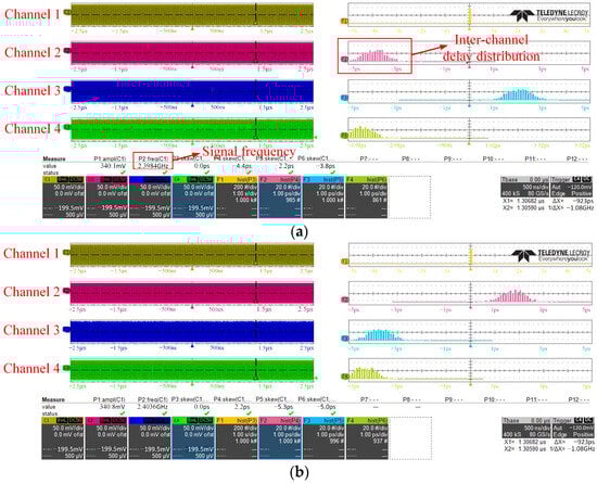
Figure 10.
Channel synchronization test: (a) Channel 1, 2, 3, and 4 synchronization test; (b) Channel 1, 5, 6, and 7 synchronization test.
To achieve multi-channel synchronization at sampling rates of up to 10 GSPS, it is necessary to place high requirements on the system clock. Next, the impact of system clock skew and clock random jitter on synchronization are analyzed. The synchronization clock network is shown in Figure 11.
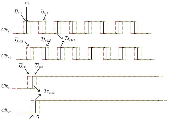
Figure 11.
Synchronous clock network.
The clocks in Figure 11 are, from top to bottom, the sampling reference clock of transceiver module 1, the sampling reference clock of transceiver module 2, the synchronous SYSREF clock of transceiver module 1, and the synchronous SYSREF clock of transceiver module 2. and have clock random jitter and , and there is clock skew between the sampling reference clocks of the modules due to the different clock paths. The SYSREF clock also has clock jitters , , , and , and clock skew .
During synchronization, the sampling reference clock of each transceiver board captures the synchronous SYSREF clock. In Figure 11, the sample reference clock of transceiver board 1 arrives at time . To ensure that the sampling reference clock successfully captures the synchronous SYSREF clock, time of arriving at the transceiver board needs to satisfy the conditions in Equation (2).
Similarly, time of arriving at the transceiver board needs to satisfy the conditions shown in Equation (3):
where is the setup time to be satisfied by the sample reference clock of the transceiver board, is the hold time during which the input signal needs to remain stable to ensure accurate signal sampling and transmission, and is the sample reference clock period of the transceiver board.
Equations (2) and (3) show that the synchronization of the system is mainly associated with sampling reference clock period, setup/hold time, and clock random jitter. The smaller the sampling reference clock frequency and the larger the period, the easier it is to synchronize; hence, synchronization at sampling rates of up to 10 GSPS is particularly difficult. The smaller the setup/hold time required for the sample reference clock, the better the system synchronization. The system setup/hold time is associated with RFSoC device characteristics and cannot be controlled. The smaller the jitter of the sampling reference clock and the synchronous SYSREF clock, the easier it is to satisfy Equations (2) and (3), and the more favorable it is to synchronize the system. Therefore, for system multi-channel synchronization at high sampling rates, controlling the reference clock jitter and synchronous SYSREF clock jitter is a key factor for successful synchronization. However, the clock with jitter is usually associated with the system hardware and cannot be controlled. When the transceiver module clock jitter is large and cannot meet the synchronization conditions, the system clock network described in Section 2.1.3 can be used to achieve a precise delay of each transceiver module synchronous SYSREF clock to meet the synchronization constraints and achieve synchronization.
Subsequently, the delay and jitter between each channel after synchronization are analyzed. The inter-channel delay and jitter are associated with the phase random jitter of the sampling reference clock, which comes from the random noise of the clock circuit, including thermal noise, flicker noise, and other kinds of superimposed independent noises. Regardless of the probability distribution of individual noise sources, the total noise obeys a Gaussian distribution according to the central limit theorem; therefore, the probability distribution of delay jitter between channels is shown in the approximate Equation (4) [17,18,19,20].
Figure 12 shows the delay distribution between two test channels and the reference channel of the high-speed oscilloscope test. From the figure, it can be seen that the delay distribution between the channels is consistent with the above analysis and approximates a Gaussian distribution.
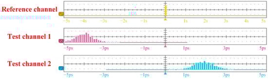
Figure 12.
Inter-channel delay distribution.
Based on the Gaussian distribution characteristics, the skew in Figure 11 is associated with the mean difference of the different channel delay jitter distributions. The smaller the mean difference, the smaller the reference clock skew between channels. The reference clock’s jitters and are associated with the variance in the Gaussian distribution. When the variance is larger and the distribution is wider, the probability of a large delay between channels is larger, and the reference clock jitter range is also larger. A large clock jitter makes it difficult to meet synchronization constraints (2) and (3), and in the DBF, generates a large sub flap and beam-pointing jitter.
Therefore, in a digital array signal processing system with high sampling rates, the variance in the delay distribution between channels directly reflects the synchronization and performance of the system.
2.2.2. Broadband Calibration Design
The frequency coverage of the signal used in this design is 1 GHz. Due to the relatively large bandwidth, the impact of frequency characteristic mismatch between multiple channels in the entire frequency band must be considered. The mismatch in frequency characteristics can lead to problems such as directional graphic changes and pulse compression into pairs of the side lobe. To correct the frequency mismatch, a broadband equalization filter is added to each channel. Channel equalization is a prerequisite for achieving broadband beamforming, and the following equalization filter is designed using the frequency method for broadband calibration [21,22,23].
The frequency response of the equalization filter of each channel to be calibrated can be calculated from the frequency response of each channel to be calibrated and the frequency response of the reference channel and that of the equalization filter of the reference channel, as shown in Equation (5).
where is the frequency response of the reference channel, is the frequency response of each channel to be calibrated, and is the frequency response of the reference channel equalization filter. There are a total of channels to be calibrated and the broadband signal used for calibration consists of sample points. Based on the algorithm in the literature [21,22,23], the plural weight of the -channel equalization filter is obtained using Equation (6).
where is the pseudo-inverse of the frequency factor array. . The frequency factor array is an M ×L matrix, and the elements of its m + 1 row and l + 1 column are shown in Equation (7).
The hardware implementation process of the broadband calibration is shown in Figure 13 and includes the FFT IP core, the IP core for the equalization filter weight coefficient calculation, the ROM for the pseudo-inverse memory, and the IP core for the equalization filter. A linear frequency modulation (LFM) signal with 1 GHz bandwidth and 11.5 GHz IF will be used as the channel calibration signal in the calibration process.
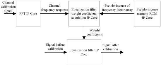
Figure 13.
Process of broadband calibration implementation.
The signal is acquired through each transceiver channel, and the acquired signal is first used to calculate the frequency response of the channel through the FFT IP core, and then the frequency response of the channel is input to the IP core of the equalization filter weight factor calculation. The IP core is designed and implemented by the XILINX High-Level Synthesis (HLS) Tool, which mainly performs the pseudo-inverse matrix multiplication of the equalization filter frequency response matrix and the frequency factor array for each channel. At the same time, the pseudo-inverse of the frequency factor array is read from the ROM and input to the weight coefficient calculation IP to finally calculate the weight coefficient of the equalization filter for the channel. The equalization filter IP core constructs a complex finite impulse response (FIR) filter based on the weight coefficients, and finally completes the construction of the equalization filter for the channel. After the broadband baseband signal passes through the filter during beamforming, the frequency mismatch can be corrected, and the channel equalization completed.
After broadband channel calibration, the calibration is tested. Figure 14 shows time-domain waveforms between channels acquired by the high-speed oscilloscope after the broadband amplitude-phase calibration.
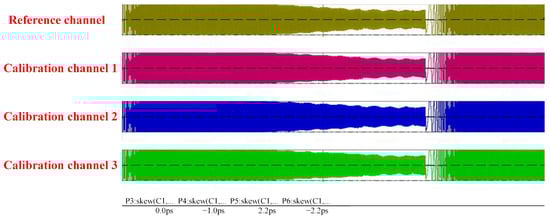
Figure 14.
Time-domain waveform after broadband calibration.
The magnitude-phase response before and after calibration is shown in Figure 15. Figure 15a shows that the amplitude error between the different channels to be calibrated is large, and the maximum difference reaches 10 dB. Figure 15b shows that the amplitude error between the channels is small, and the maximum difference is only 0.5 dB. The results verify that the proposed method can achieve broadband calibration.
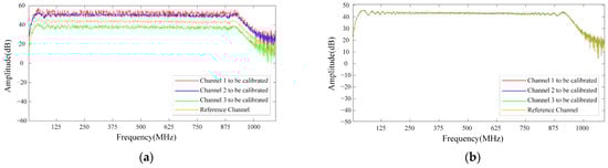
Figure 15.
Comparison of amplitude-frequency responses before and after broadband calibration: (a) Amplitude-frequency responses between channels before broadband calibration; (b) Amplitude-frequency responses between channels after broadband calibration.
3. Implementation and Verification of the DBF Algorithm
3.1. Principle and Simulation of the MIMO Phased Array DBF Algorithm
The MIMO phased array radar is a combination of conventional MIMO radar and phased-array radar with the advantages of MIMO radar without sacrificing the coherent processing gain of phased-array radar. The essence of the technology is to divide the transmit array into several subarrays that are allowed to overlap, where each subarray transmitting waveforms orthogonal to the other subarray transmits waveforms based on the weight vector. This technique allows for the optimal design of the emission direction map or emission waveform of a MIMO radar to concentrate the emission energy to the region of interest, thus effectively improving the detection and tracking performance of the radar system [24,25,26].
The array used in this algorithm validation has a total of 11 array elements and the array is divided into four 8-element subarrays through full overlap subarray division, as shown in Figure 16.
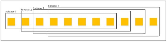
Figure 16.
Array element arrangement.
Based on the subarray division method described above, each subarray emits mutually orthogonal waveforms and emission beamforming, with each beam pointing at different angles. The directional maps of the subarrays are simulated, in which four subarrays point in four directions −45°, −15°, 15°, and 45°. Results of the directional map simulation are shown in Figure 17.
Figure 17.
Directional map simulation.
3.2. Hardware Implementation of the MIMO Phased Array DBF Algorithm
For hardware implementation, the operating band range is 11–12 GHz, with a bandwidth of 1 GHz. The baseband signals of each subarray are orthogonal to each other and can be either LFM signals or single-frequency signals.
The hardware implementation of the MIMO phased array digital multibeam formation algorithm consists of the following parts: DBF weight calculation IP core, multiplier, baseband signal ROM, multi-stage flow accumulation module, and IF signal ROM module. The implementation process includes two clock domains: fast and slow. To ensure hardware timing convergence, DBF weight calculations, including multiplication, addition, and other computational operations, are performed in the slow clock domain, while the high-speed and broadband IF signal emission is realized in the fast clock domain. Of these, the DBF weight calculation IP is designed and generated by the XILINX HLS tool [27]; however, the specific design process is not the focus of this paper and will not be described.
The flow chart of the hardware implementation of the MIMO phased array DBF algorithm is shown in Figure 18.
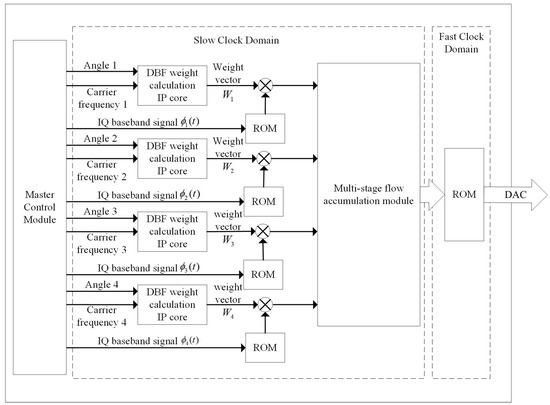
Figure 18.
Hardware implementation of the algorithm.
The four parallel DBF weight calculation IP cores in Figure 18 calculate the one-dimensional DBF weights of each subarray based on the beam pointing angle and carrier frequency from the master control module. A two-dimensional full overlap emission beamforming matrix is constructed based on the DBF weights of the four subarrays as follows:
where is the weight corresponding to the ’th array element of the ’th subarray.
At the same time, the master module passes the mutually orthogonal baseband IQ signals required for the ’th subarray to the transceiver module and stores them in the ROMs of the baseband signal. During beamforming, the transceiver module reads the baseband signals in each ROM and constructs the input signal matrix .
The multiplication of the full-overlap transmit beamforming matrix with the input signal matrix is achieved using a four-channel parallel complex multiplier and a multi-stage flow accumulation module in Figure 18 [26].
The output signal of the 11 array elements can be obtained as shown in Equation (11).
When the module detects a new incoming baseband signal or a new beam pointing angle and carrier frequency, the above calculation is repeated to obtain the latest output signal matrix. Finally, the output signal of each array element is output to the IF signal cache ROM, and a higher frequency clock is used in the fast clock domain to transmit the IF signal from the ROM cache to realize the hardware implementation of the simultaneous multibeam algorithm.
The DBF results were tested in a microwave darkroom; the test environment is shown in Figure 19. Corresponding to the system hardware architecture in Section 2.1.1, ① in Figure 19 is the system transmit antenna array, ② is the system RF front-end, ③ is the system digital array signal processor and ④ is the receiving antenna turntable, which can be rotated in any azimuth angle. The receiving antenna is connected to the spectrum analyzer and vector network analyzer to test the transmit signal.
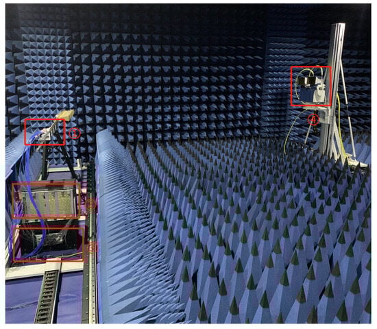
Figure 19.
Testing environment.
Four beams pointing at −45°, −15°, 15°, and 45° are generated simultaneously, with carrier frequencies of 8.1 G, 8.2 G, 8.3 G, and 8.4 G, respectively. Turning the angle of the receiving antenna turntable in Figure 19 to point to different angles shows the received multibeam spectrum in Figure 20. The corresponding transmit beam spectrum obtained when the turntable is turned to −45° is shown in Figure 20a. The energy of the carrier frequency of 8.1 GHz, which corresponds to −45°, is the largest. Similarly, Figure 20b shows that when the receiving antenna turntable is turned to 15°, the energy of the carrier frequency of 8.3 GHz corresponding to 15° is the maximum. Therefore, the beam can be pointed in the correct direction, consistent with the simulation results, and realize the MIMO phased array DBF algorithm.
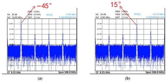
Figure 20.
Transmitting beam spectrum: (a) Spectrum pointing to −45 degrees; (b) Spectrum pointing to 15 degrees.
4. Conclusions
Based on the on-chip RF integrated system chip, this paper adopted the HIF architecture to design an all-digital, low-power, multi-channel, high-speed broadband digital array signal processing system with 64 receive channels and 64 transmit channels in a small size, forming a hardware platform for multi-channel radar system applications. Through hardware implementation and verification of the broadband MIMO phased array digital multi-beam formation algorithm, the designed system can achieve simultaneous multi-channel sampling and amplitude and phase calibration with a high sampling rate and large bandwidth and has a high performance of broadband digital array signal processing, which verifies the feasibility and engineering value of the design described in this paper.
Author Contributions
Conceptualization, G.X. and Z.S.; methodology, G.X. and Z.S.; software, G.X. and Z.S.; validation, G.X. and Z.S.; formal analysis, G.X.; investigation, Z.S.; resources, G.X.; data curation, Z.S.; writing—original draft preparation, G.X. and Z.S.; writing—review and editing, Y.Q. and B.W.; visualization, G.X.; supervision, G.L.; project administration, G.X.; funding acquisition, G.L. All authors have read and agreed to the published version of the manuscript.
Funding
This work was supported by the Science Funds for Distinguished Young Scholars of Shannxi Province under Grant 2021JC-23.
Data Availability Statement
Not applicable.
Conflicts of Interest
The authors declare no conflict of interest.
References
- Arnieri, E.; Boccia, L.; Amendola, G.; Glisic, S.; Mao, C.; Gao, S.; Rommel, T.; Penkala, P.; Krstic, M.; Yodprasit, U.; et al. An integrated radar tile for digital beamforming X-/Ka-band synthetic aperture radar instruments. IEEE Trans. Microw. Theory Tech. 2019, 67, 1197–1206. [Google Scholar] [CrossRef]
- Despoisse, T.; Ghiotto, A.; Busson, P.; Deltimple, N. A comparison of beamforming schemes for 5G mm-wave small cell transmitters. In Proceedings of the 2018 16th IEEE International New Circuits and Systems Conference (NEWCAS), Montreal, QC, Canada, 24–27 June 2018. [Google Scholar]
- Coutinho, V.A.; Ariyarathna, V.; Coelho, D.F.G.; Pulipati, S.K.; Cintra, R.J.; Madanayake, A.; Bayer, F.M.; Dimitrov, V.S. A low-SWaP 16-beam 2.4 GHz digital phased array receiver using DFT approximation. IEEE Trans. Aerosp. Electron. Syst. 2020, 56, 3645–3654. [Google Scholar] [CrossRef]
- Curtis, D.D.; Thomas, R.W.; Payne, W.J.; Weedon, W.H.; Deaett, M.A. 32-channel X-band digital beamforming plug-and-play receive array. In Proceedings of the IEEE International Symposium on Phased Array Systems and Technology, Boston, MA, USA, 14–17 October 2003. [Google Scholar]
- Mao, C.-X.; Gao, S.; Tienda, C.; Rommel, T.; Patyuchenko, A.; Younis, M.; Boccia, L.; Arnieri, E.; Glisic, S.; Yodprasit, U.; et al. X/Ka-band dual-polarized digital beamforming synthetic aperture radar. IEEE Trans. Microw. Theory Tech. 2017, 65, 4400–4407. [Google Scholar] [CrossRef]
- Song, Y.-J.; Lim, S.-J.; Lee, S.-K.; Jang, J.-S. Adaptive digital beamforming for uplink coverage enhancement in 5G NR system. In Proceedings of the 2019 27th Telecommunications Forum (TELFOR), Belgrade, Serbia, 26–27 November 2019. [Google Scholar]
- Aldowesh, A.; Alnuaim, T.; Alzogaiby, A. Slow-moving micro-UAV detection with a small scale digital array radar. In Proceedings of the 2019 IEEE Radar Conference (RadarConf), Boston, MA, USA, 22–26 April 2019. [Google Scholar]
- Codau, C.; Buta, R.; Pastrav, A.; Palade, T.; Dolea, P.; Puschita, E. ULA transmit beamforming on SDR platform. In Proceedings of the 2020 International Workshop on Antenna Technology (iWAT), Bucharest, Romania, 25–28 February 2020. [Google Scholar]
- Patyuchenko, A.; Younis, M.; Krieger, G.; Wang, Z.; Gao, S.; Qin, F.; Mao, C.; Glisic, S.; Debski, W.; Boccia, L.; et al. Highly integrated dual-band digital beamforming synthetic aperture radar. In Proceedings of the 2015 European Radar Conference (EuRAD), Paris, France, 9–11 September 2015. [Google Scholar]
- Wu, B.; Quan, Y.; Xiao, G.; Li, Y.; Xing, M. Design of high-IF DBF system based on RF transceiver. Syst. Eng. Electron. 2022, 44, 365–375. [Google Scholar]
- Pozdnyakov, I.Y.; Turkanov, G.I.; Negrov, D.V. Reconfigurable and scalable architecture of a system for digital processing of broadband radar signals. J. Commun. Technol. Electron. 2017, 62, 229–235. [Google Scholar] [CrossRef]
- Liang, Z.; Liu, Q.; Long, T. A novel subarray digital modulation technique for wideband phased array radar. IEEE Trans. Instrum. Meas. 2020, 69, 7365–7376. [Google Scholar] [CrossRef]
- Farley, B.; Erdmann, C.; Vaz, B.; McGrath, J.; Cullen, E.; Verbruggen, B.; Pelliconi, R.; Breathnach, D.; Lim, P.; Boumaalif, A.; et al. A programmable RFSoC in 16nm FinFET technology for wideband communications. In Proceedings of the 2017 IEEE Asian Solid-State Circuits Conference (A-SSCC), Seoul, Republic of Korea, 6–8 November 2017. [Google Scholar]
- Feng, Z.; Yao, Y.; Gao, D. Low power structure digital up converter design for software radio system. J. Circuits Syst. Comput. 2020, 30, 2150019. [Google Scholar] [CrossRef]
- Boulogeorgos, A.-A.A.; Kapinas, V.M.; Schober, R.; Karagiannidis, G.K. I/Q-imbalance self-interference coordination. IEEE Trans. Wirel. Commun. 2016, 15, 4157–4170. [Google Scholar] [CrossRef]
- Jenq, Y.-C. Direct digital synthesizer with jittered clock. IEEE Trans. Instrum. Meas. 1997, 46, 653–655. [Google Scholar] [CrossRef]
- Towfic, Z.J.; Sayed, A.H. Clock jitter estimation in noise. In Proceedings of the 2011 IEEE International Symposium of Circuits and Systems (ISCAS), Rio de Janeiro, Brazil, 15–18 May 2011. [Google Scholar]
- Liu, L.; Pokharel, R. Compact modeling of phase-locked loop frequency synthesizer for transient phase noise and jitter simulation. IEEE Trans. Comput.-Aided Des. Integr. Circuits Syst. 2016, 35, 166–170. [Google Scholar] [CrossRef]
- IEEE Std 2414-2020; IEEE Standard for Jitter and Phase Noise. IEEE: New York City, NY, USA, 2021; pp. 1–42.
- Peng, X.; Zhang, Y.; Wang, W.; Yang, S. Broadband mismatch calibration for time-interleaved ADC based on linear frequency modulated signal. IEEE Trans. Circuits Syst. I Regul. Pap. 2021, 68, 3621–3630. [Google Scholar] [CrossRef]
- Shao, T.; Wang, Z.; Fang, S.; Liu, H.; Chen, Z.N. A full-passband linear-phase band-pass filter equalized with negative group delay circuits. IEEE Access 2020, 8, 43336–43343. [Google Scholar] [CrossRef]
- Lee, J.; Uhm, M.S.; Park, J.H. Synthesis of a self-equalized dual-passband filter. IEEE Microw. Wirel. Compon. Lett. 2005, 15, 256–258. [Google Scholar]
- Reza, A.; Muttaqin, H.; Miftachul, U. Phased-MIMO radar: Angular resolution. IOP Conf. Ser. Mater. Sci. Eng. 2021, 1125, 012046. [Google Scholar] [CrossRef]
- Hassanien, A.; Vorobyov, S.A. Phased-MIMO radar: A tradeoff between phased-array and MIMO radars. IEEE Trans. Signal Process. 2010, 58, 3137–3151. [Google Scholar] [CrossRef]
- Chen, Y.-J.; Zhang, Q.; Luo, Y.; Li, K.-M. Multi-target radar imaging based on phased-MIMO technique—Part I: Imaging algorithm. IEEE Sens. J. 2017, 17, 6185–6197. [Google Scholar] [CrossRef]
- Chen, Y.-J.; Zhang, Q.; Luo, Y.; Li, K.-M. Multi-target radar imaging based on phased-MIMO technique—Part II: Adaptive resource allocation. IEEE Sens. J. 2017, 17, 6198–6209. [Google Scholar] [CrossRef]
- Pei, X.; Wang, N.; Werthimer, D.; Duan, X.F.; Li, J.; Ergesh, T.; Liu, Q.; Cai, M.H. Design of RFSoC-based digital phased array feed (PAF) and hybrid architecture beamforming system. Res. Astron. Astrophys. 2022, 22, 045016. [Google Scholar] [CrossRef]
Disclaimer/Publisher’s Note: The statements, opinions and data contained in all publications are solely those of the individual author(s) and contributor(s) and not of MDPI and/or the editor(s). MDPI and/or the editor(s) disclaim responsibility for any injury to people or property resulting from any ideas, methods, instructions or products referred to in the content. |
© 2023 by the authors. Licensee MDPI, Basel, Switzerland. This article is an open access article distributed under the terms and conditions of the Creative Commons Attribution (CC BY) license (https://creativecommons.org/licenses/by/4.0/).