Abstract
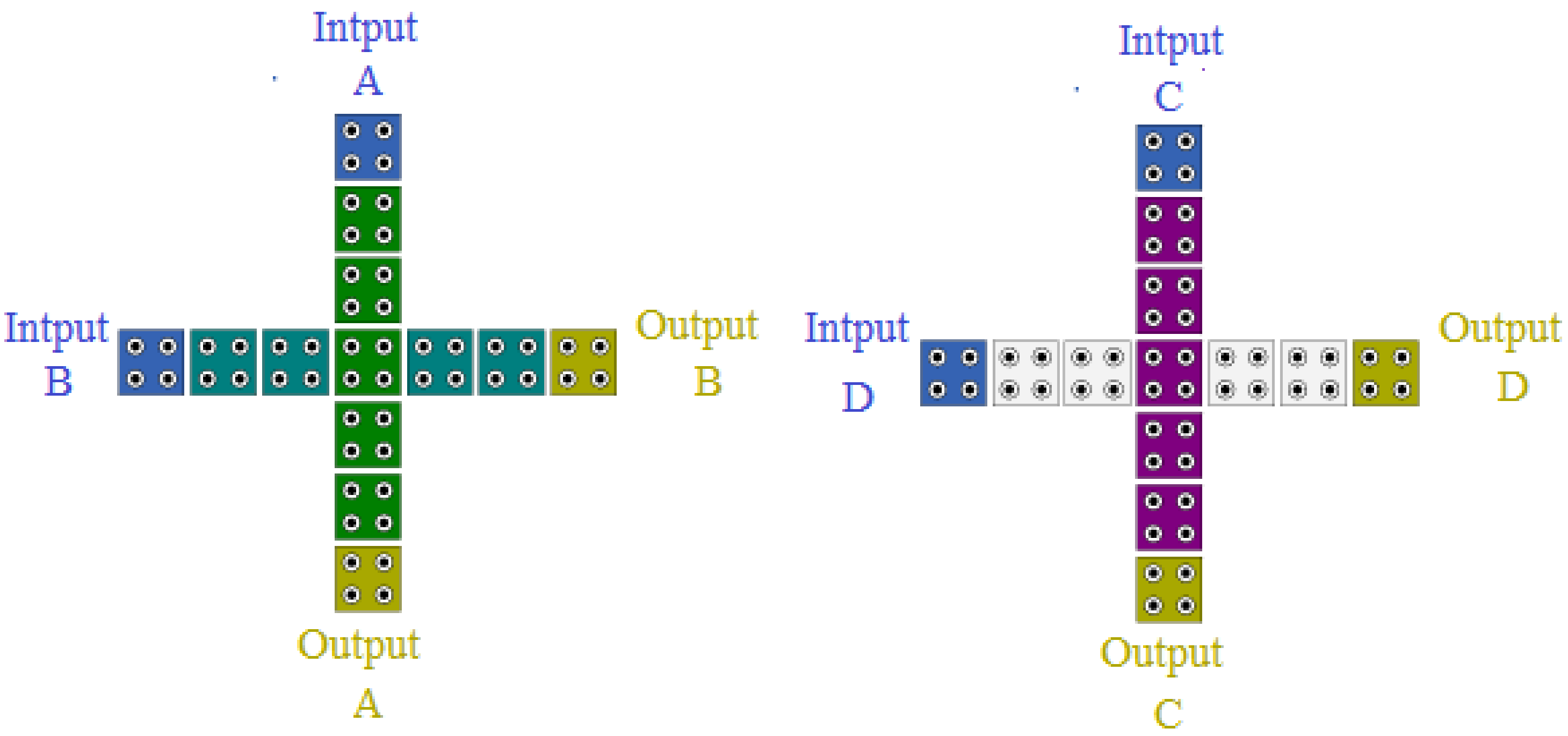
Reversible logic enables ultra-low power circuit design and quantum computation. Quantum-dot Cellular Automata (QCA) is the most promising technology considered to implement reversible circuits, mainly due to the correspondence between features of reversible and QCA circuits. This work aims to push forward the state-of-the-art of the QCA-based reversible circuits implementation by proposing a novel QCA design of a reversible full adder\full subtractor (FA\FS). At first, we consider an efficient XOR-gate, and based on this, new QCA circuit layouts of Feynman, Toffoli, Peres, PQR, TR, RUG, URG, RQCA, and RQG are proposed. The efficient XOR gate significantly reduces the required clock phases and circuit area. As a result, all the proposed reversible circuits are efficient regarding cell count, delay, and circuit area. Finally, based on the presented reversible gates, a novel QCA design of a reversible full adder\full subtractor (FA\FS) is proposed. Compared to the state-of-the-art circuits, the proposed QCA design of FA\FS reversible circuit achieved up to 57% area savings, with 46% and 29% reduction in cell number and delay, respectively.
Keywords:
reversible gates; Feynman gate; Toffoli gate; Peres gate; PQR gate; TR gate; RUG gate; URG gate; RQCA gate; RQG gates; reversible FA\FS 1. Introduction
Moore’s Law is ending, and even newly delivered deep-submicron transistors cannot satisfy the high demand from the consumer electronics market for high-speed and low-power computing [1]. Therefore, conventional computing paradigms [2] are now being rethought and alternative approaches considered, such as unconventional number systems [3], reversible computing [4], and nano-electronics [5], at different design levels. Reversible computation plays a significant role in the exciting journey of designing ultra-low power systems for future applications [6]. It can perform lossless energy computation, avoiding energy dissipation during computation. In addition, reversible gates have equal numbers of inputs and outputs, with a one-to-one mapping between inputs and outputs, resulting in zero information loss and the capability to achieve inputs from outputs [7]. However, the most critical problem is efficiently designing and implementing reversible computing circuits.
Quantum-dot cellular automata (QCA) is one of the most promising technologies for reversible logic implementation [8]. QCA can be propounded as a potential alternative and candidate for scalability restrictions of complementary metal-oxide–semiconductor (CMOS) technology [9]. It uses nano-level interactions to implement digital logic with low energy consumption and high clocking frequency. The advancements in fabrication [10,11] and simulation [12,13] of QCA circuits have enabled researchers to design complete computational circuits [14]. Thus, the unique features of QCA, including zero power dissipation in an ideal situation with reversible logic, can lead to the design of low-power consumption circuits that can fulfill the requirements of future technology [15].
This paper focuses on designing and implementing efficient reversible circuits based on QCA technology. The critical element is to achieve efficient QCA reversible gates, which can be used to design high-performance reversible circuits. In that direction, we designed a new low-area, high-speed QCA implementation of the XOR gate, which is the core of most reversible gates in the XOR operation. Moreover, reversible gates, including Feynman, Toffoli, Peres, PQR, TR, RUG, URG, RQCA, and RQG gates, were efficiently designed and implemented with QCA. Finally, the proposed QCA-based RQG and Feynman reversible gates were used to design a unified reversible Full Adder\Full Subtractor (FA\FS), i.e., the basis for digital processors’ data paths. Additionally, since one of the difficulties with the fabrication of QCA circuits is multi-layer crossing [10,16], the proposed circuits were designed in a coplanar QCA form.
The rest of this paper is organized as follows. Firstly, the background on QCA technology and reversible gates is presented in Section II. The proposed QCA reversible circuits are presented in Section III. Section IV evaluates the performance of the proposed designs and circuits, and finally, Section V concludes the paper.
2. Background
2.1. Sustainable Computing
Sustainable computing is a computing paradigm that concerns zero environmental impact as a form of heat, energy, or any other polluting substance. It has different meanings, but what we mean by sustainable computing is reducing energy consumption and increasing the number of operations per second [17]. In other words, what we mean by sustainability is reducing energy consumption or bringing it close to zero. In modern-day computing, the energy consumption of computers and cell phones is increasing exponentially due to big data and heavy processing; this process should be stopped by replacing the current technologies. The increasing amount of processing also produces more heat. The presence of millions of devices and computing elements in a limited and small space on the integrated circuits causes each chip to generate hundreds of watts of heat and disperse it in the working space. To address this overheating and energy consumption, Landauer [18] showed that the loss of every bit of information dissipates the energy of KTxln2 joules, where K is Boltzmann’s constant and T is the absolute temperature. Theoretically, it is possible to approach 100% reuse by using reversible computations and logic instead of irreversible computations and logic. That is, an ideal system should only be turned on initially and then run forever on recycled electricity [17]. Reversible logic says that it is possible to reduce the energy loss during a circuit to zero if it is possible to reach from the final states to the primary states, irrespective of what is happening along the path. In this logic, one can stop at any stage of the route, return to the previous floors, and access the entrances of the circuit. In other words, the outputs are an injective function of the inputs, and each input can be produced from the outputs. Reversible circuits are used to achieve reversible calculations and logic. Hence, by transferring energy between reversible circuits and thermodynamically separating them, it is possible to create reversible circuits that both produce little heat and use little power. Current computing elements (irreversible computing elements) are unstable; As a result, we will soon run out of energy or need solutions to cool the circuits and computing devices. To reach higher performance levels, a new path should be used instead of the current path. Therefore, reversible computing and circuits are the only way out of this possible problem [19] because reversible computing dissipates very little heat and consumes minimal power. It is considered the best sustainable computing for the computer hardware industry.
2.2. Reversible Computing
Digital logic gates used in conventional logic circuits are irreversible, and these circuits lose information for each processing. As a result, they generate some heat per processing due to data loss. Thus, according to the second law of thermodynamics and Landauer’s principle, it is impossible with irreversible computing to forever make energy more efficient.
In 1982, Edward Fredkin and Tommaso Toffoli proposed a novel type of gate that was utterly reversible [20]. Providing reversibility requires that reversible gates have as many inputs as outputs, even if some inputs remain directly unchanged. Reversibility means that no information is lost; as a result, entropy is unchanged, and heat is not lost. Therefore, reversibility means no energy is wasted as heat during computational and logical operations (although one still has to worry about other sources of energy dissipation). On the other hand, new nanotechnologies, such as QCA technology, enable calculations with very low energy loss. As a result, it is a promising candidate for reversible logic implementation [17].
2.3. Quantum-Dot Cellular Automata
The quantum-dot cellular automata technology is based on QCA cells, where each cell at a nanoscale level represents one logical bit. Information is stored as electrons’ charge, corresponding to the electronic configuration of the QCA cell. Each QCA cell consists of two electrons; Columbic effects can shape two distinct polarizations, corresponding to the logic zero and one. QCA cells are typically represented with a square and four dots containing two electrons, which can freely move between dots, as shown in Figure 1 [21]. Two electrons can assume six different conditions in these holes, but some are not allowed due to Coulombic interactions and the principle of maximum distance between charges. Therefore, the Coulombic repulsion forces two electrons to be placed in diagonal positions; each one of the two states can represent binary logic, zero and one [22]. As depicted in Figure 1, the polarizations −1 and +1 represent the binary logic 0 and 1, respectively [23]. Figure 2 also shows the standard QCA wire. This QCA wire is created using standard QCA cells (90-degree cells) [24].
Figure 1.
The QCA cells [23,24].
Figure 2.
Schematic of a standard QCA wire [24].
At the junction of two wires, QCA crossovers are used. There are several ways to create crossovers. Coplanar crossovers using non-adjacent clock phases are among the best and most stable methods due to the use of standard cells (90° cells). Two different types of crossovers are shown in Figure 3 [16].
Figure 3.
Wire coplanar crossovers.
Figure 4 presents a four-phase clocking scheme for QCA. It can be observed that during the first phase, the cell is unpolarized, affected by Coulombic interactions between neighbor cells. By increasing the barrier, the cell is polarized based on the input drivers, and then, at the end of this phase, the barrier is heightened enough to prevent tunneling. Therefore, the state of the cell is locked and remains fixed. Note that the switching happens in this phase. The barrier is kept high during the second phase, the ‘hold.’ During this phase, the cell is stable, and data is transferred to the neighbor cells. During the third phase, the ‘release’, barriers decrease gradually, and the cell becomes unstable. At this phase, the cell data is not needed anymore, becoming unpolarized and entering the Relax phase. In this fourth last phase, the barriers are at the minimum level, and the cell is unpolarized. After this, the cell is ready to return to the Switching phase [24].
Figure 4.
Clock phases in QCA [24].
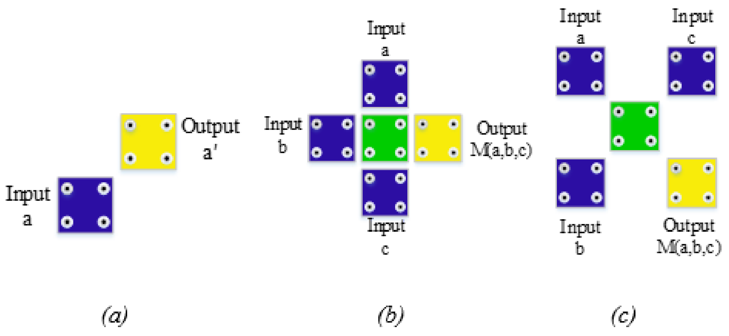
The basic NOT-gate, a gate that inverts the logic value, can be implemented in QCA by the low-cost configuration shown in Figure 5a. Besides, the majority gate is the essential QCA gate, as shown in Figure 5b,c.
Figure 5.
(a): NOT-gate configurations in the QCA based on 90° cells, (b) original QCA majority gate, and (c) rotated QCA majority gate [21].
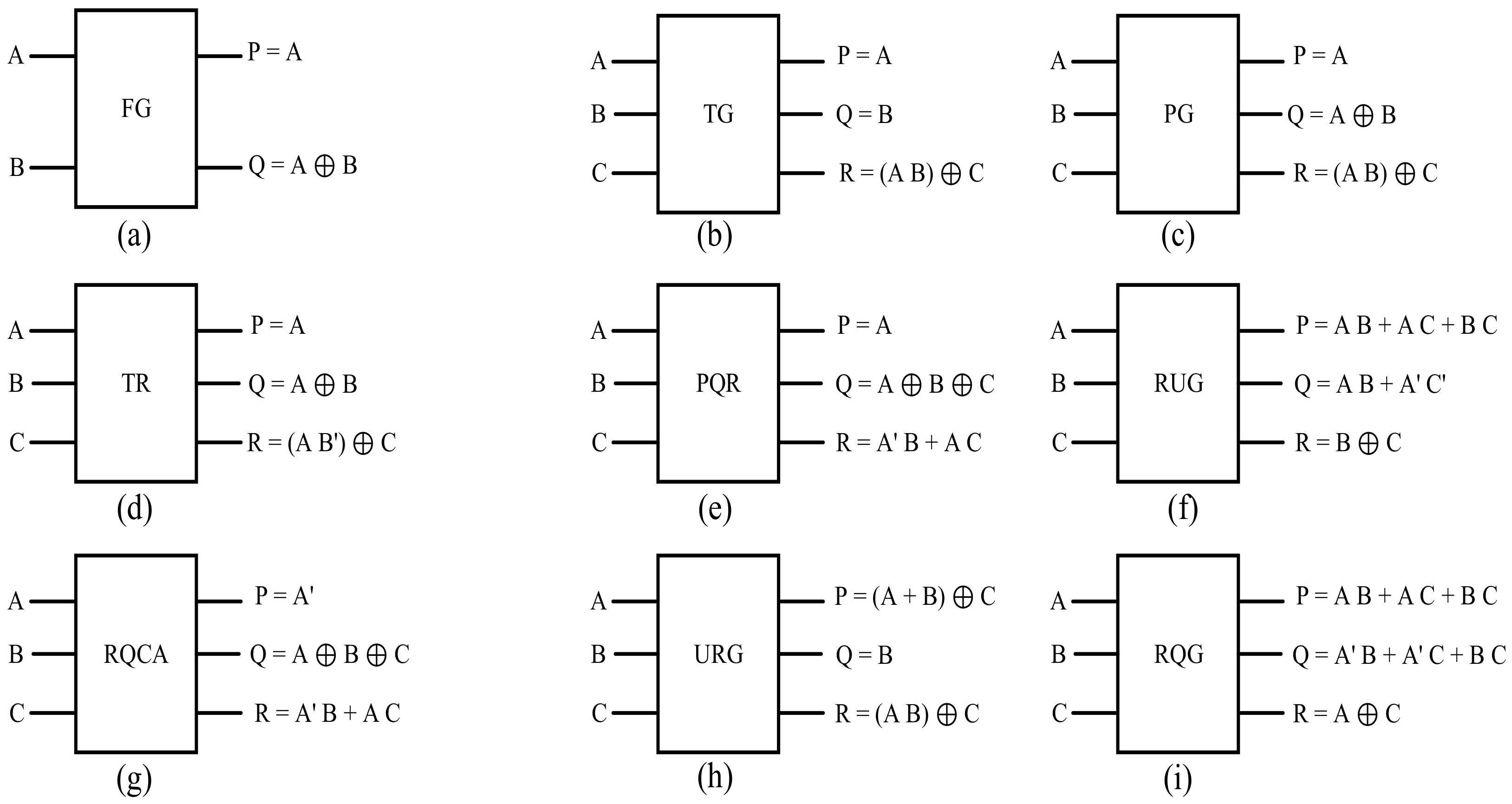
To this point, distinct reversible gates for circuit design considering different applications have been introduced. The block diagram and corresponding logic functions of basic logic gates are shown in Figure 6, including the PQR [25], the Feynman gate (FG) [26], the Toffoli gate (TG) [27], the Peres gate (PG) [28], the TR [29], the RUG [30], the RQCA [31], the URG [32], and the RQG [33]. The FG is also known as a controller since for A = 0, the output Q is B, and for A = 1, it is the invert of B. TG is a complete gate since two inputs are accessible from the output side. Moreover, the PG can be used as a half adder (HA) since, for C = 0, we have Q = A⊕B and R = AB.
Figure 6.
Reversible gates: (a): Feynman gate [26], (b): Toffoli gate [27], (c): Peres gate [28], (d): TR gate [29], (e): PQR gate [25], (f): RUG gate [30], (g): RQCA gate [31], (h): URG gate [32], (i): RQG gate [33].
3. The Proposed Circuits
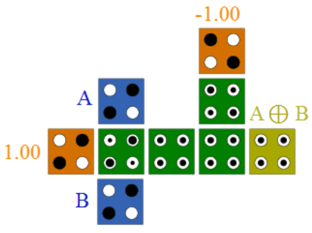
The main aim of this work is to design efficient QCA reversible gates, including Feynman, Toffoli, Peres, PQR, TR, RUG, URG, RQCA, and RQG gates. In order to achieve this aim, from the XOR gate (Figure 7) [34] and, based on the proposed basic logic circuits, a Full Adder\Full Subtractor was designed. We show that all these circuits have better performance and efficiency, considering the number of cells, area, and delay. They also allow designs on a single layer without any rotated cells.
Figure 7.
XOR gate.
3.1. Implementation of the Proposed Reversible Gates
The most well-known, applicable reversible gates in practice are depicted in Figure 6. Almost all of them are supported on the XOR-gate, which becomes the most essential and critical gate for designing efficient reversible circuits. In this section, we design and implement different reversible gates with QCA technology, using the XOR gate (Figure 7), and coplanar realization results in efficient QCA implementation of the reversible gates FG, TG, PG, PQR, TR, RUG, URG, RQCA, and RQG. The proposed implementations are pushing forward QCA-based reversible computing since they are the most crucial reversible gates and are fundamental on many reversible circuits, including arithmetic and logic units (ALU).
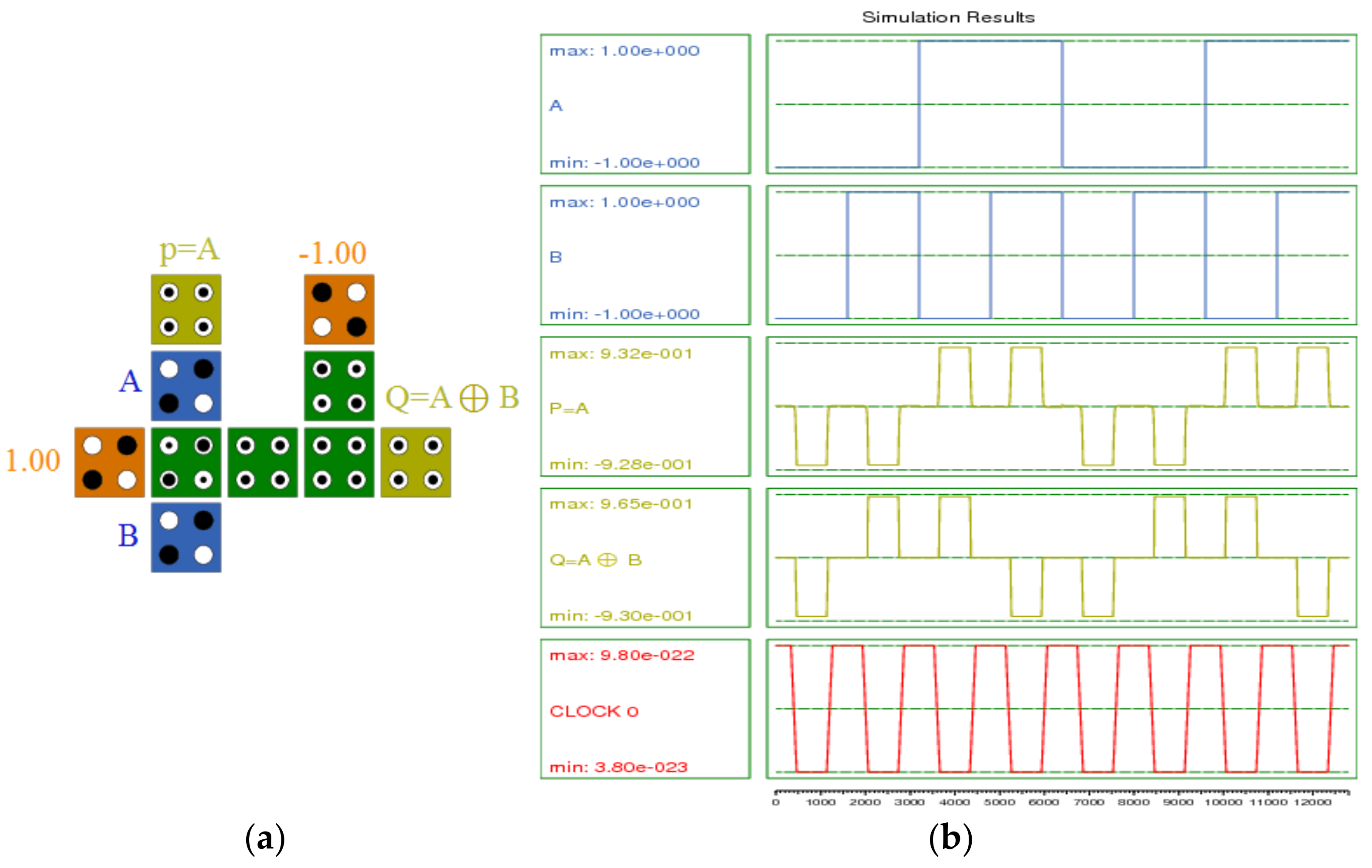
The proposed QCA implementation of the Feynman gate (FG) is shown in Figure 8a. The FG consists of two inputs and two outputs. In this gate, A and B are the inputs, and P and Q are the outputs. It relies on a QCA wire to transfer the input A to the output and an XOR gate to produce the output Q. The QCA Designer simulation results (Figure 8b) show that the proposed gate leads to a 0.25 clock delay at the cost of 10 cells for the Feynman gate.
Figure 8.
(a) QCA layout and (b) simulation results for the proposed Feynman gate.
The Toffoli gate (TG) consists of three inputs and three outputs. A, B, and C are the inputs, and P, Q, and R are the outputs. Figure 9 shows the block diagram of this gate. We propose two new QCA layouts for the TG gate in Figure 10a,b. Figure 10a shows the first proposed design. The proposed-a QCA-based TG relies on two direct QCA wires and a rotated QCA majority gate [10] for calculating the AND operation followed by the XOR gate, as depicted in Figure 7. Figure 10b also shows the second proposed design. The proposed-b QCA-based TG relies on two direct QCA wires and a generic QCA majority gate for calculating the AND operation followed by the XOR gate as depicted in Figure 7. The simulation results for the proposed TG are presented in Figure 10c. The output delays of both layouts are precisely the same. Therefore, the results of both simulations are the same. Thus, only one of the simulation results is shown in Figure 10c.
Figure 9.
The Toffoli gate QCA Design.

Figure 10.
(a) and (b) QCA layout, and (c) simulation results for the proposed Toffoli gate.
The Peres gate (PG) consists of three inputs and three outputs. In this gate, A, B, and C are the inputs, and P, Q, and R are the outputs. Figure 11 shows the block diagram of this gate. We propose two new QCA layouts for the PG gate in Figure 12a,b. Figure 12a shows the first proposed (proposed-a) design. The proposed PG1 was implemented based on the circuit presented in Figure 12a. A wire and an XOR gate produced the first and second outputs. In addition, a generic QCA majority gate with two XORs was used to make the third output. Figure 12b also shows the dual proposed design. The proposed PG2 was implemented based on the circuit presented in Figure 12b. A wire and an XOR gate produced the first and second outputs. In addition, a rotated QCA majority gate with two XORs was used to make the third output. The simulation results for the proposed TG are presented in Figure 12c. The output delays of both layouts are precisely the same. Therefore, the results of both simulations are the same, and thus only one of the simulation results is given in Figure 12c.
Figure 11.
The Peres gate QCA Design.
Figure 12.
(a) and (b) QCA layout, and (c) simulation results for the proposed Peres gate.
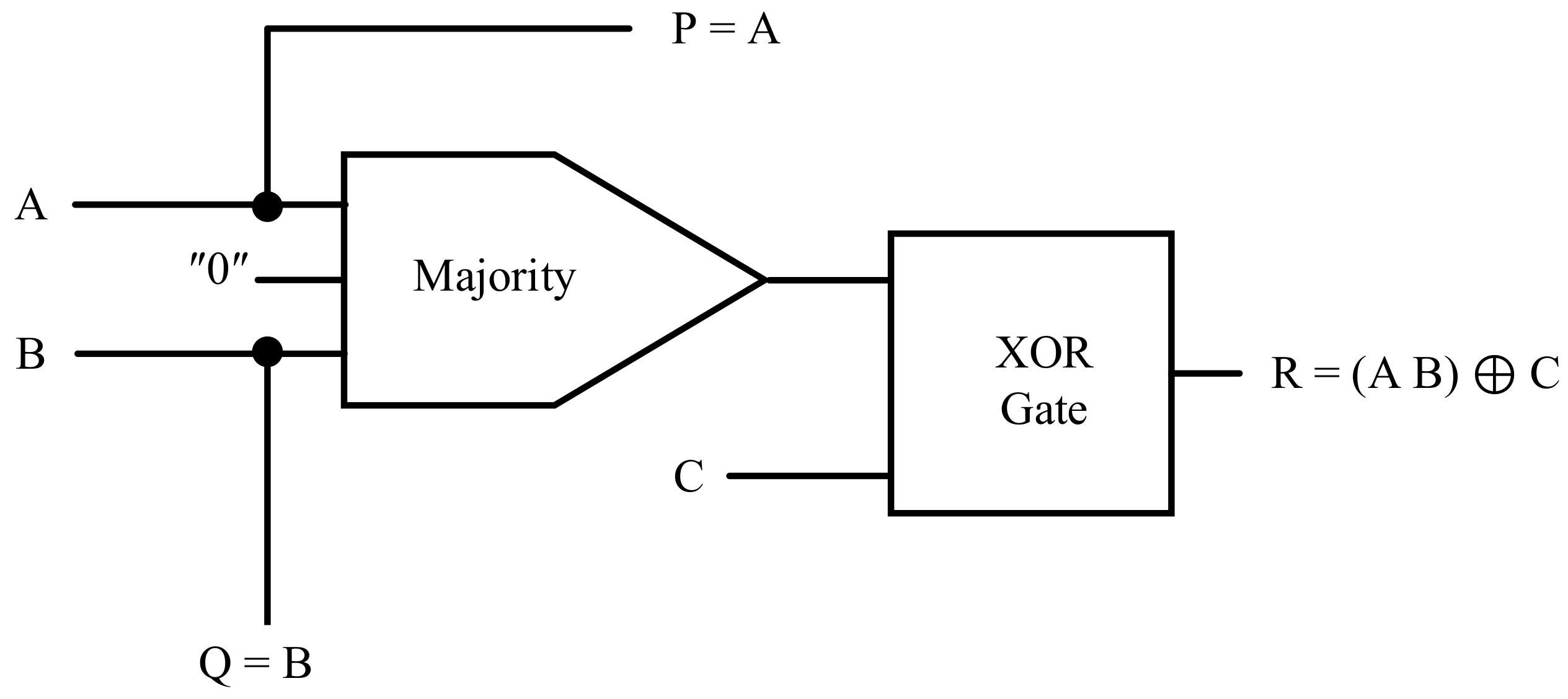
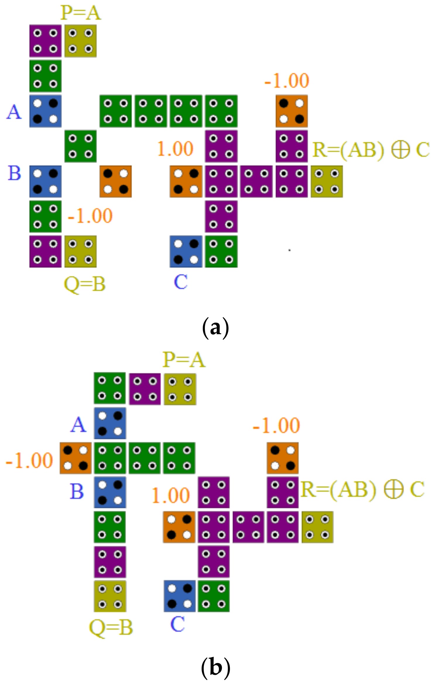
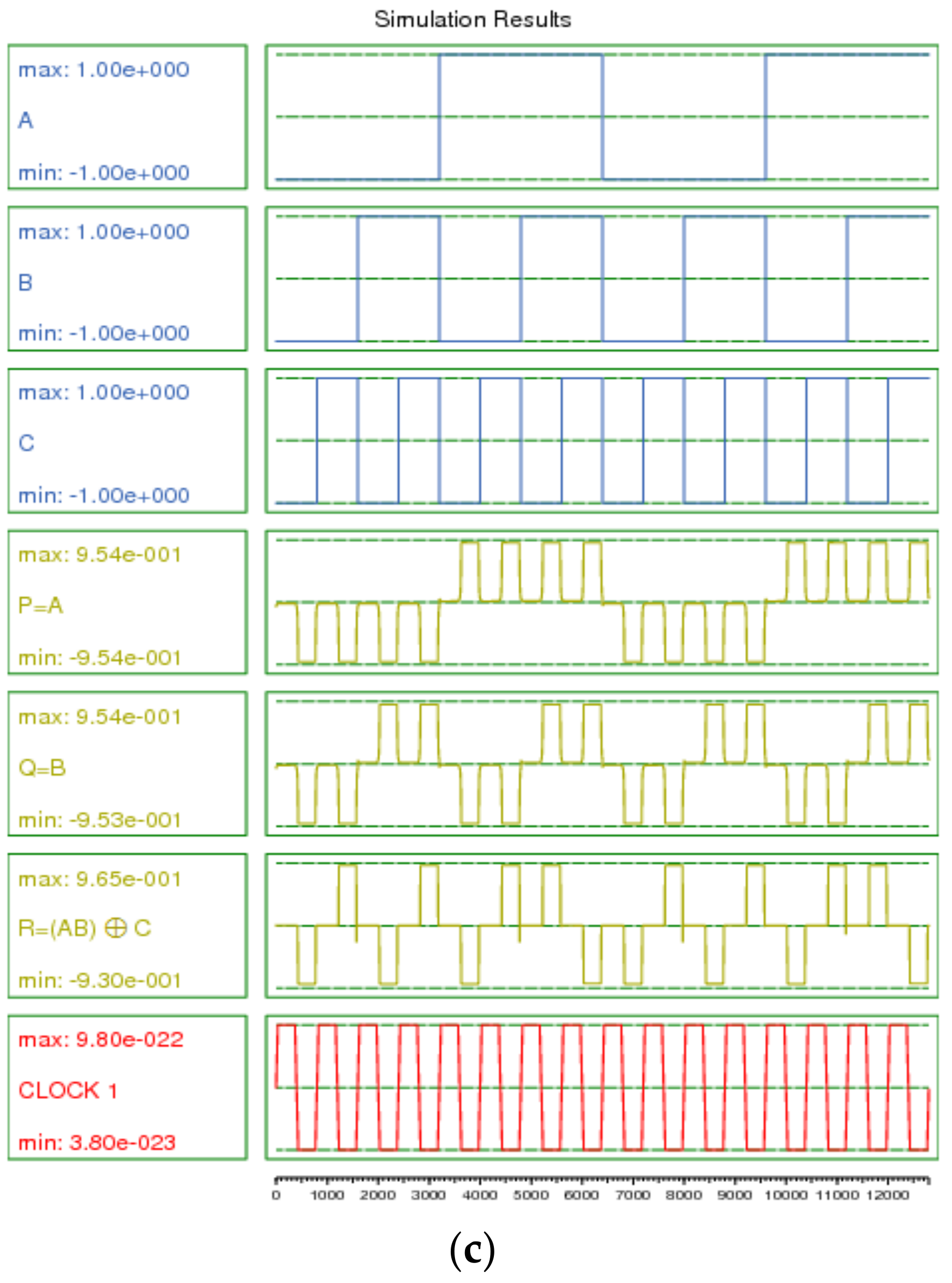
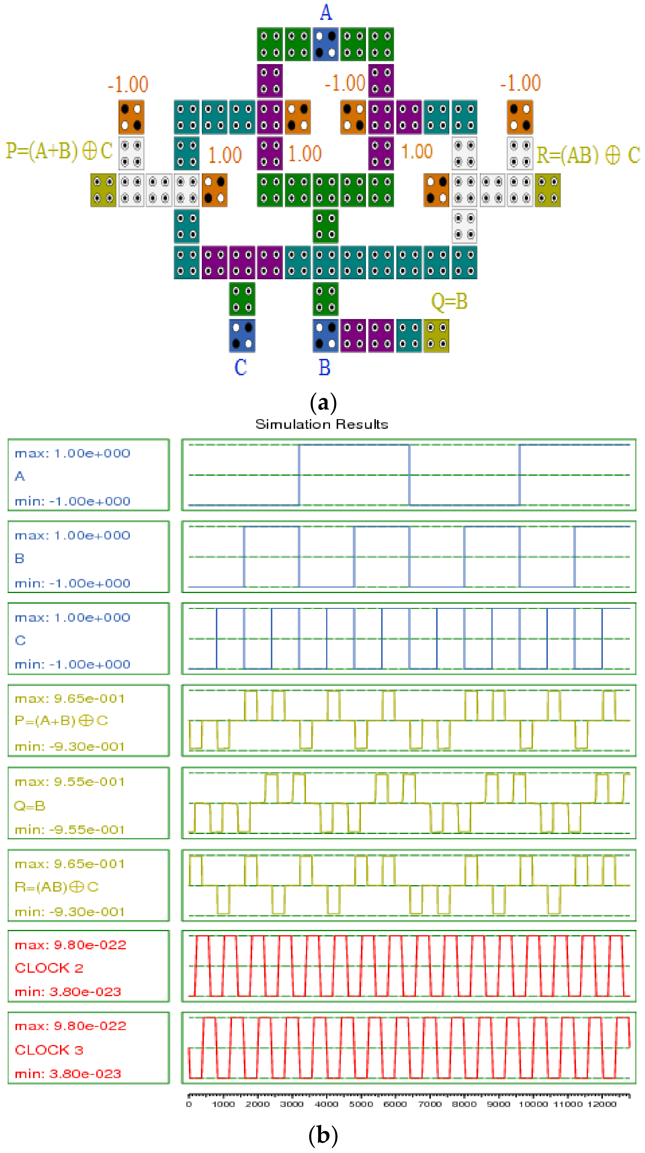
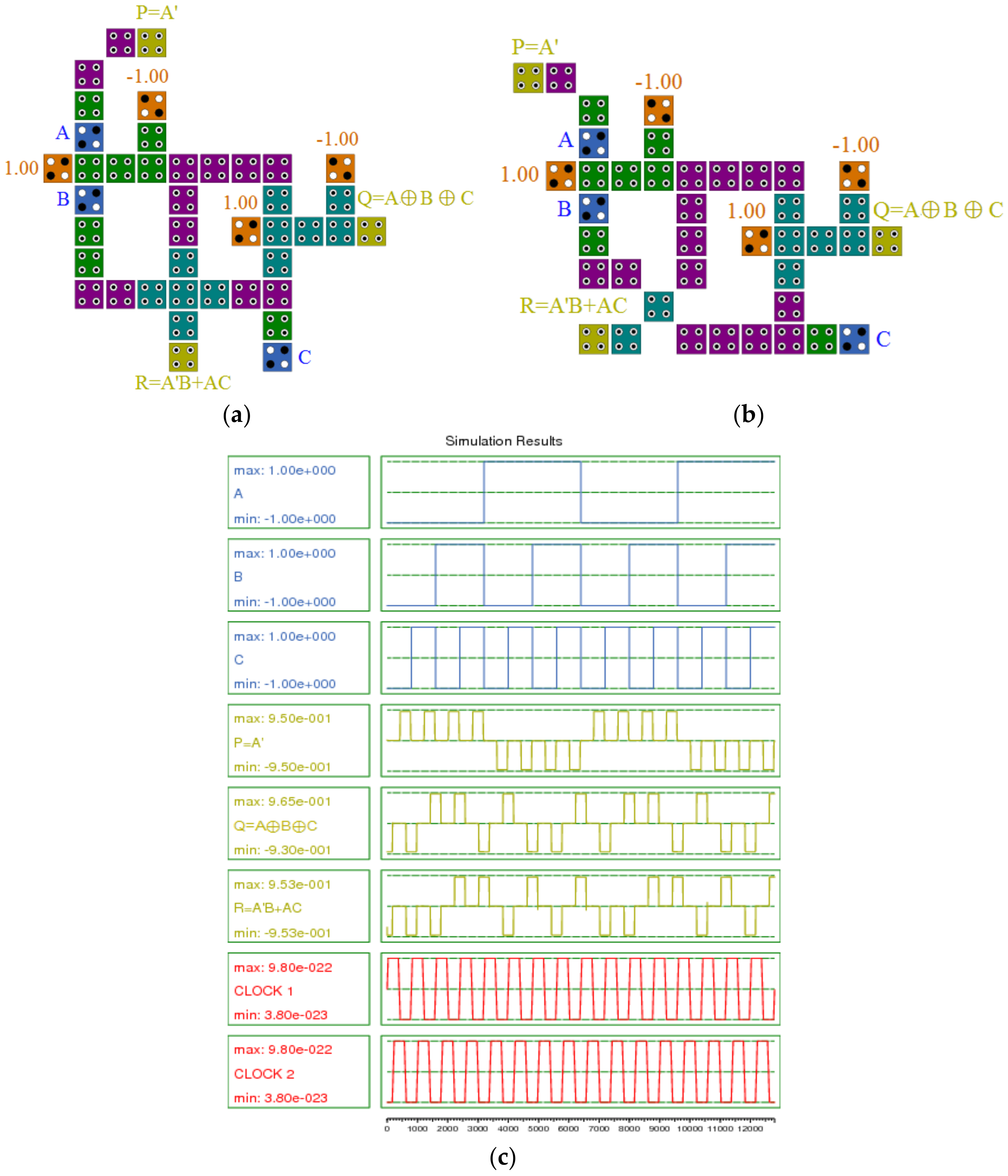
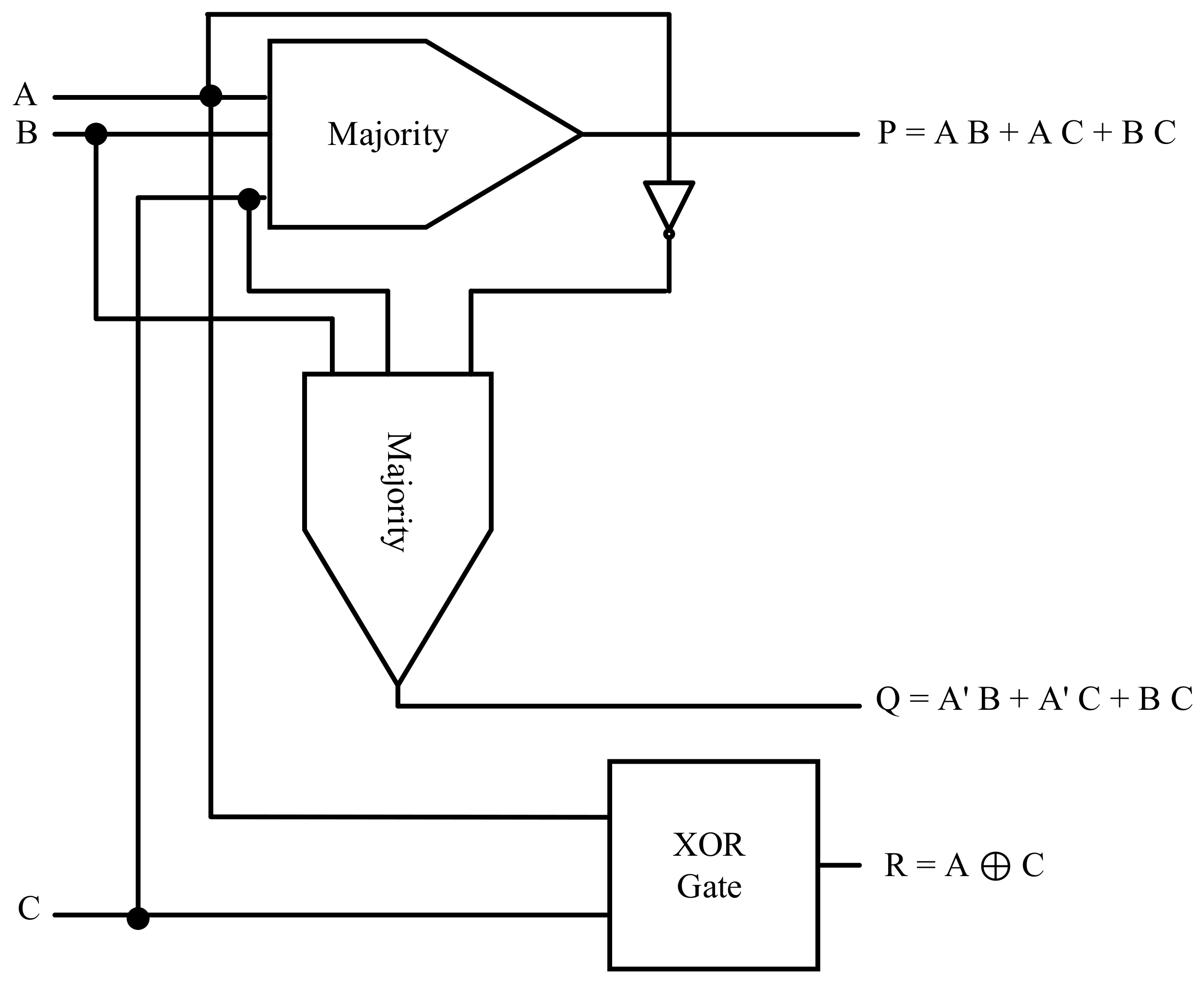
The PQR gate consists of three inputs and three outputs, where A, B, and C are the inputs, and P, Q, and R are the outputs. Figure 13 shows the structure of the proposed PQR gate, which is similar to the one proposed in [26] except for the XOR architecture. We suggest two new QCA layouts of the PQR gate in Figure 14a,b. The proposed cell placement in Figure 14 results in a crossover-free layout with just 40 (a and b) cells and a delay of 0.75 clock cycles. Figure 14a shows the first proposed (proposed-a) design. The proposed PQR-a gate was implemented based on the design presented in Figure 14a. A wire produced the first output, and two XOR gates produced the second output. In addition, a rotated QCA majority gate was used to make the third output. Figure 14b also shows the dual proposed design. The proposed PQR-b gate was implemented based on the design presented in Figure 14b. A wire produced the first output, and two XOR gates produced the second output. In addition, a generic QCA majority gate was used to make the third output. The simulation results for the proposed PQR are presented in Figure 14c. The output delays of both layouts are precisely the same. Therefore, the results of both simulations are the same, and thus only one of the simulation results is given in Figure 14c.
Figure 13.
The PQR gate QCA Design.

Figure 14.
(a) and (b) QCA layout, and (c) simulation results for the proposed PQR gate.
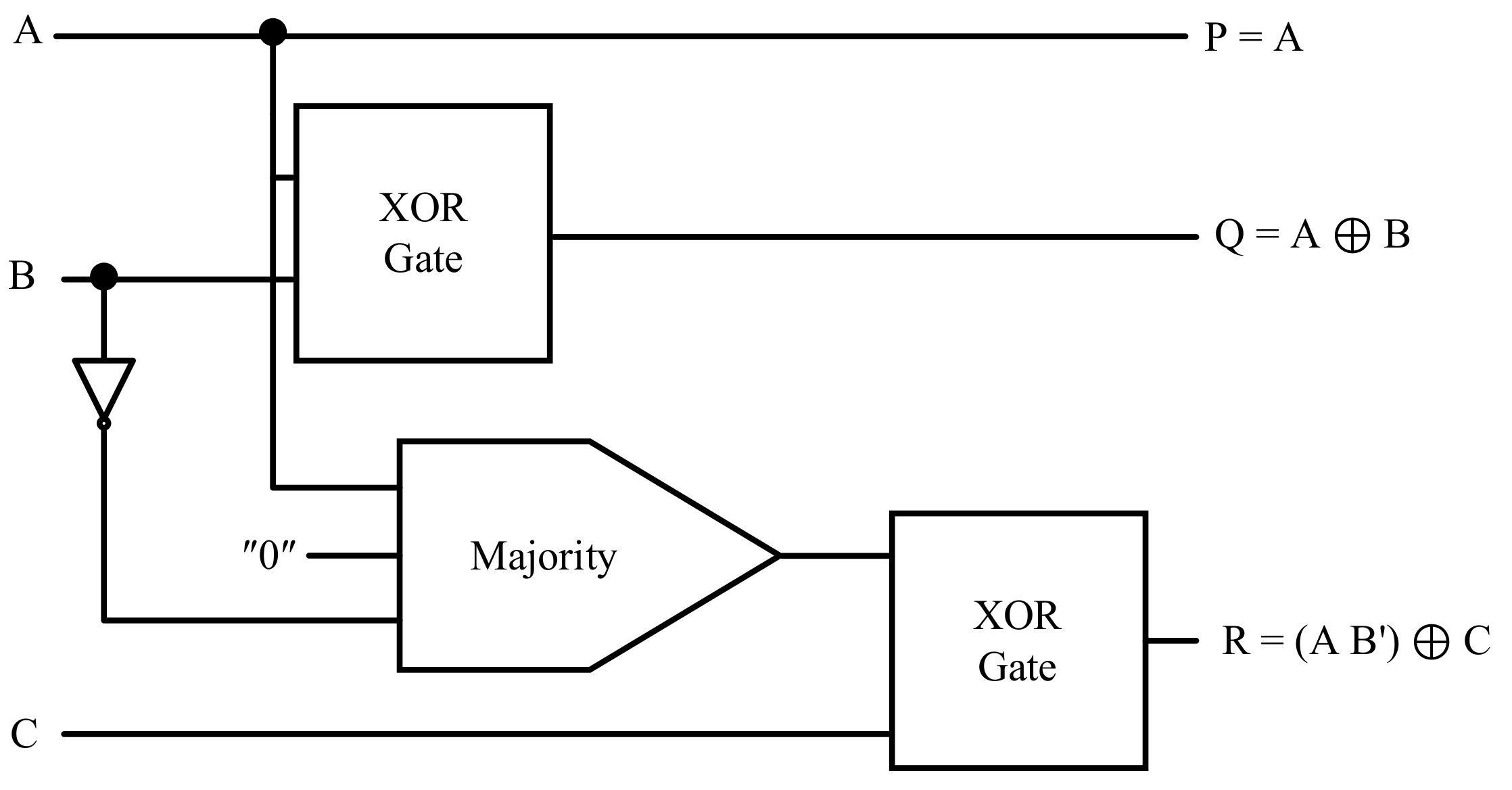
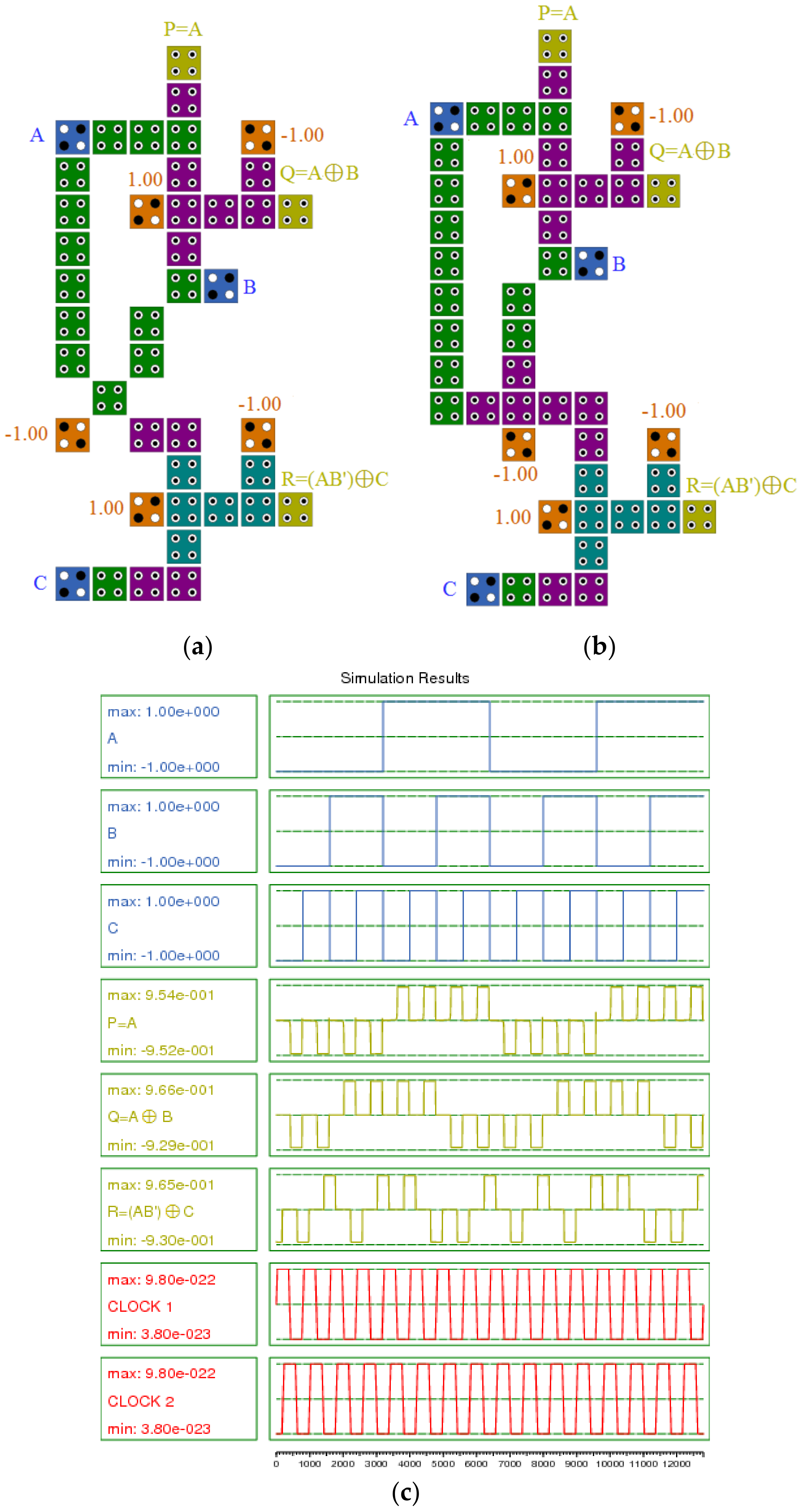
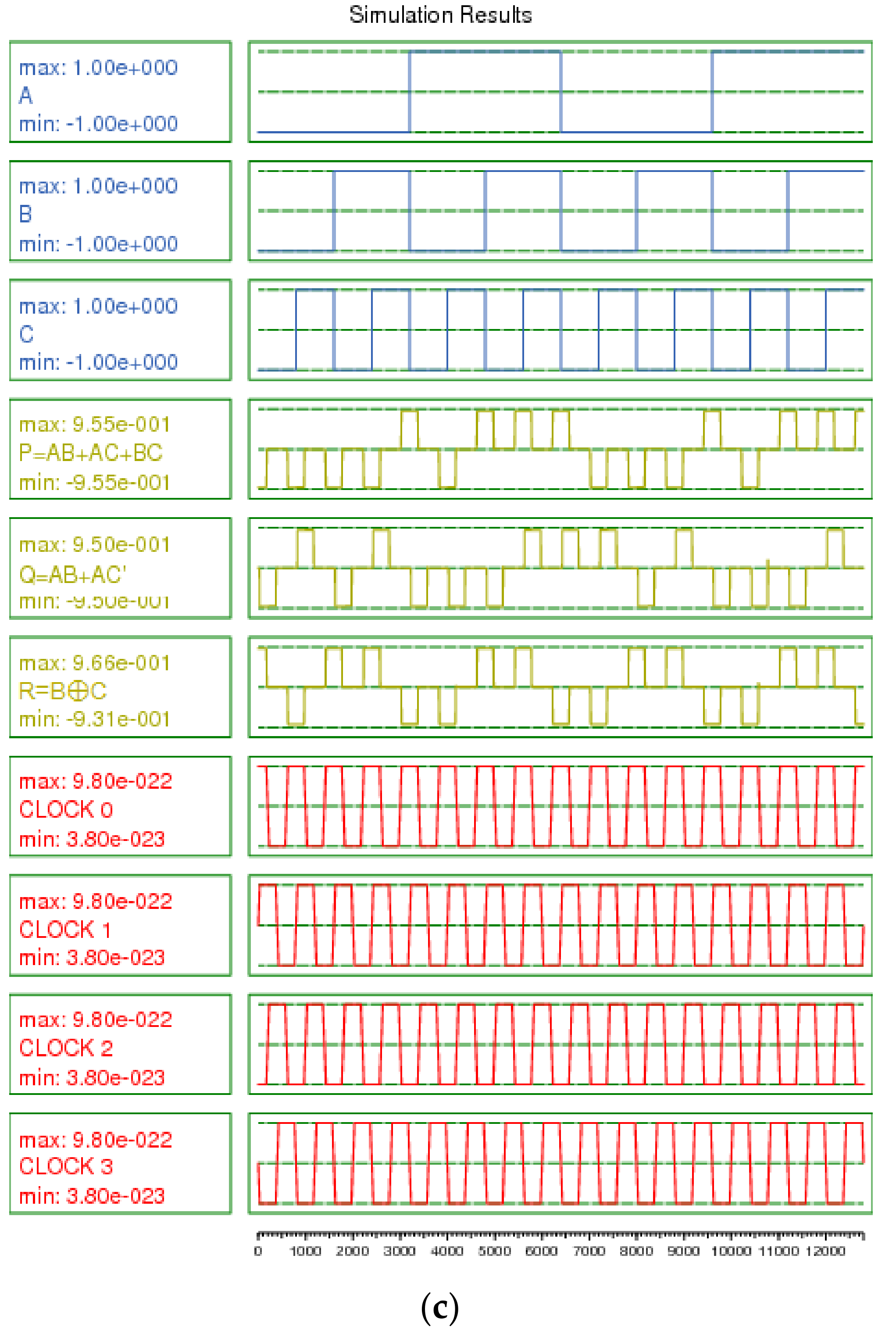
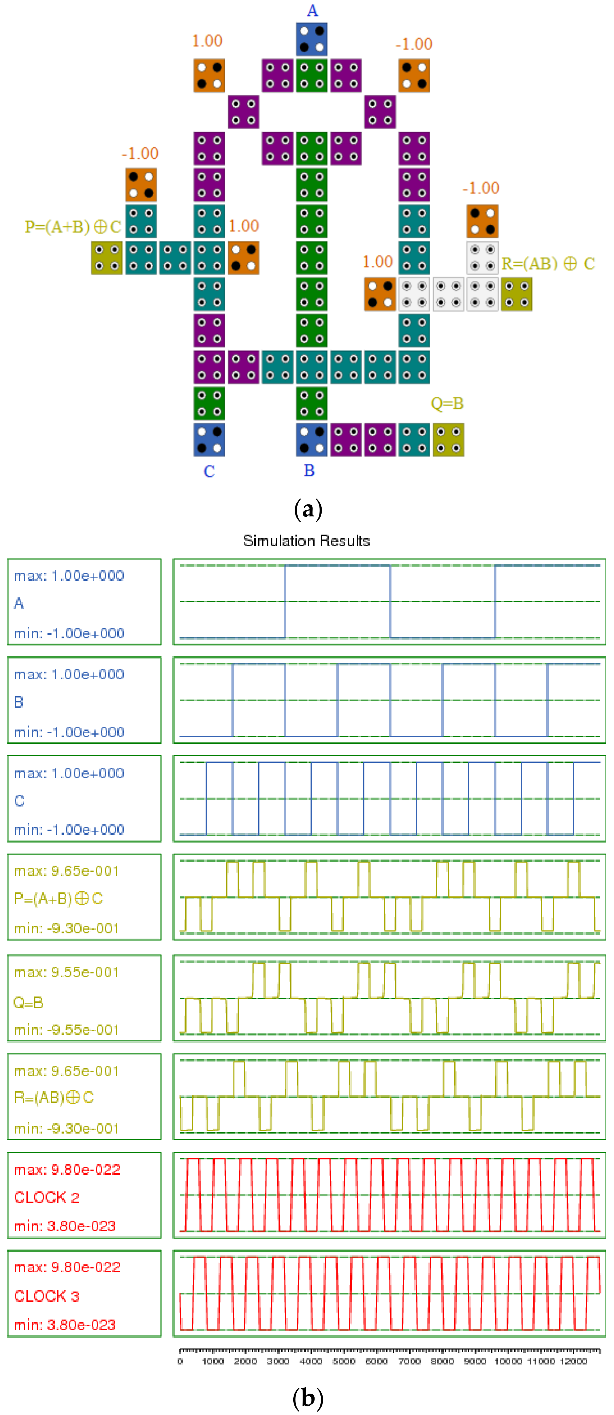
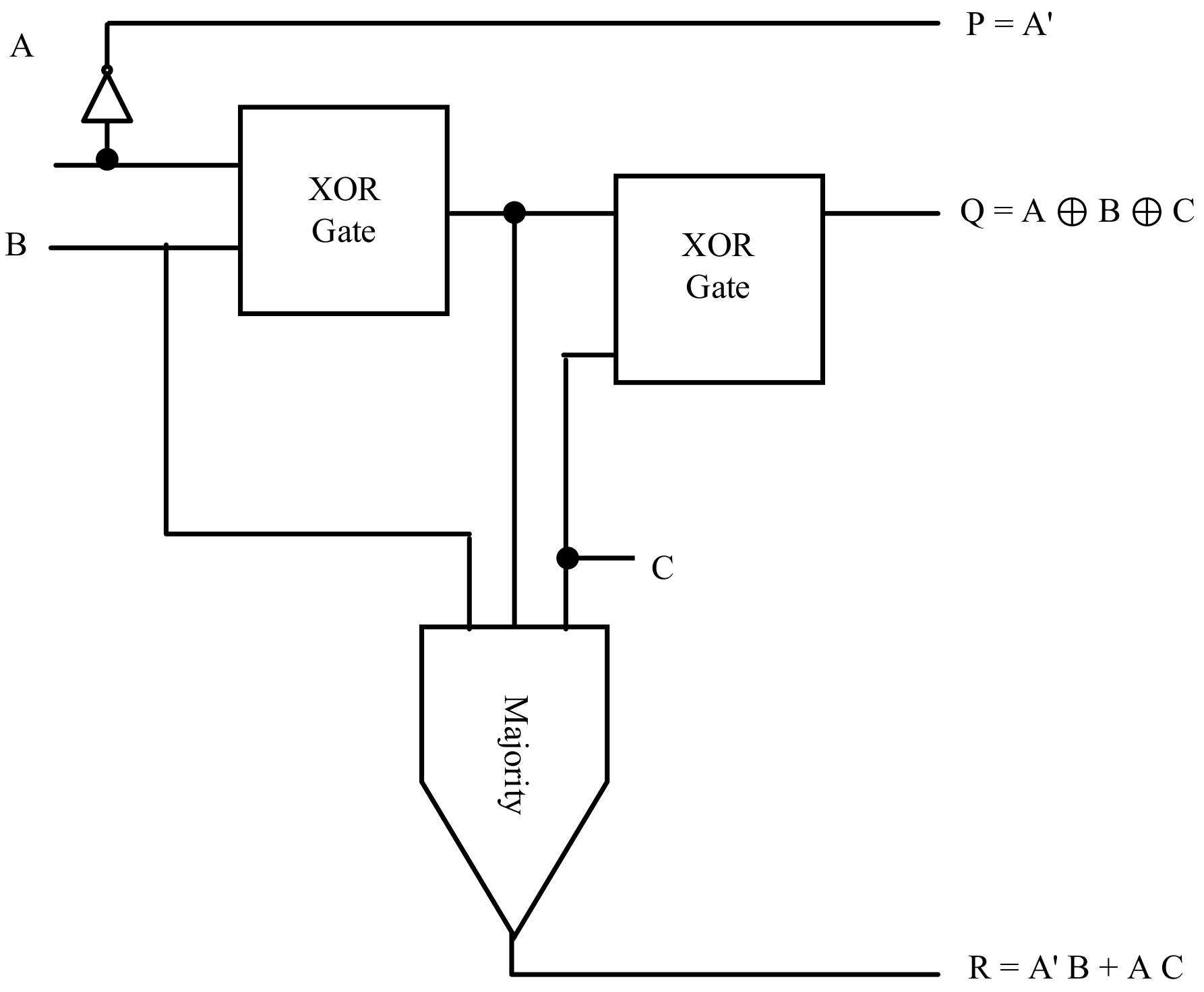
The TR gate also consists of three inputs and three outputs. In this gate, A, B, and C are the inputs, and P, Q, and R are the outputs. The TR gate requires two XOR gates, a majority, and a NOT gate, as indicated in Figure 15. We have proposed two new QCA layouts for the TR gate in Figure 16a,b. The proposed QCA implementation for the TR gate is shown in Figure 16a,b, with a delay of just 0.75 clock cycles (Figure 16c). Figure 16a shows the first proposed TR gate, which was implemented based on the design presented in Figure 16a. A wire produced the first output, and an XOR gate produced the second output. In addition, a rotated QCA majority gate and an XOR gate were used to make the third output. Figure 16b also shows the second proposed design of this gate. The proposed-b TR gate was implemented based on the design presented in Figure 16b. A wire produced the first output, and an XOR gate produced the second output. In addition, a generic QCA majority gate and an XOR gate were used to make the third output. The simulation results for the proposed TR are presented in Figure 16c. The output delays of both layouts are precisely the same. Therefore, the results of both simulations are the same, and thus only one of the simulation results is given in Figure 16c.
Figure 15.
The TR gate QCA Design.
Figure 16.
(a) and (b) QCA layout, and (c) simulation results for the proposed TR gate.
The RUG gate also consists of three inputs and three outputs, where A, B, and C are the inputs, and P, Q, and R are the outputs. Four majority and XOR gates are required to design a RUG gate, as proposed in Figure 17. The suggested cell placement and its simulation are presented in Figure 18. We have proposed two new QCA layouts for the RUG gate in Figure 18a,b. Figure 18a shows the first proposed design of this gate, which was implemented based on the design presented in Figure 18a. A rotated QCA majority gate produced the first output, and three rotated QCA majority gates and two NOT gates produced the second output. In addition, an XOR gate was used to make the third output. Figure 18b shows the dual proposed design of this gate, which was implemented based on the design presented in Figure 18b. A generic QCA majority gate produced the first output, and three original QCA majority gates and two NOT gates produced the second output. In addition, an XOR gate was used to make the third output. The simulation results for the proposed RUG are presented in Figure 18c. The output delays of both layouts are precisely the same. Therefore, the results of both simulations are the same, and thus only one of the simulation results is given in Figure 18c.
Figure 17.
The RUG gate QCA Design.

Figure 18.
(a) and (b) QCA layout, and (c) simulation results for the proposed RUG gate.
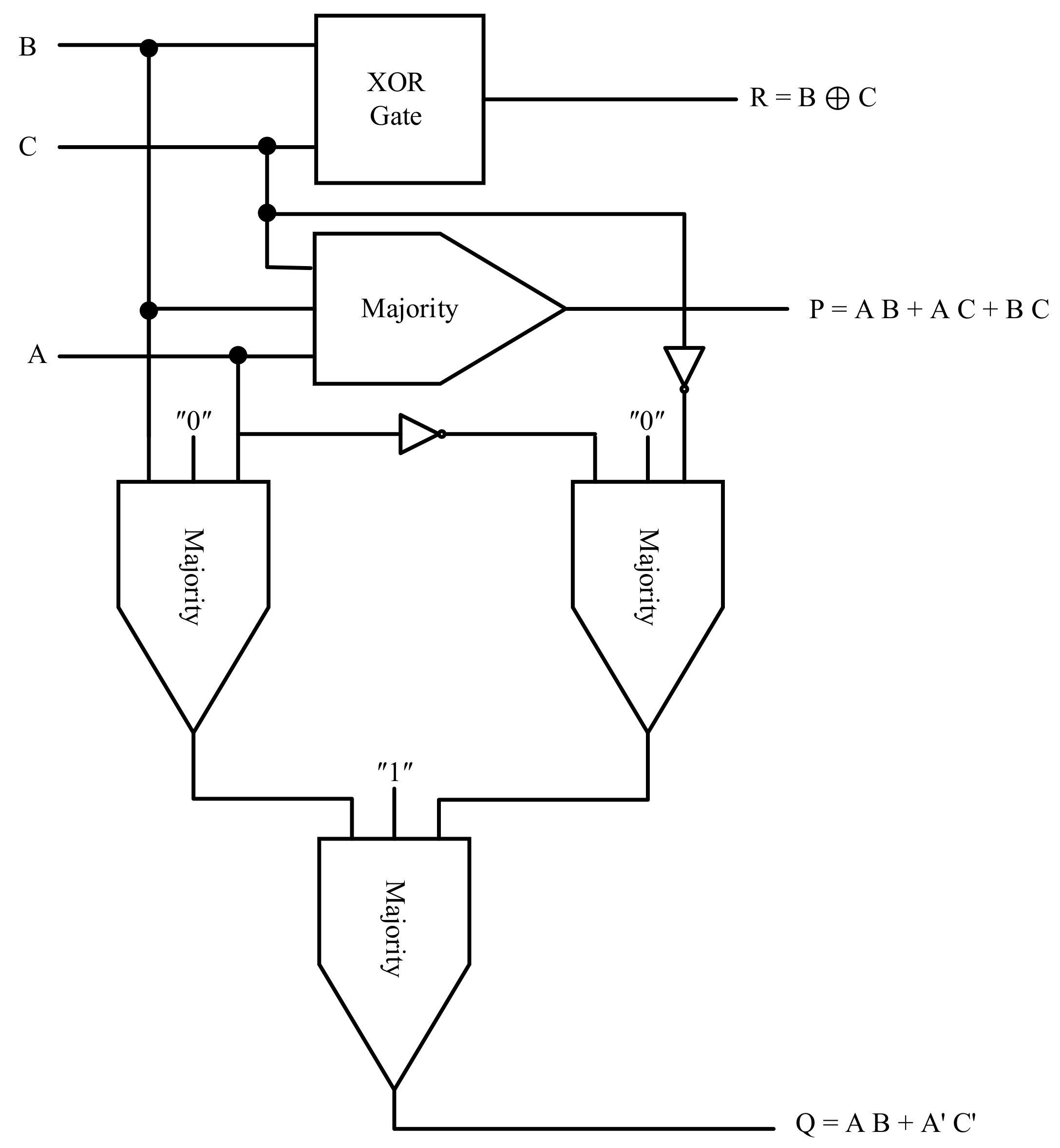
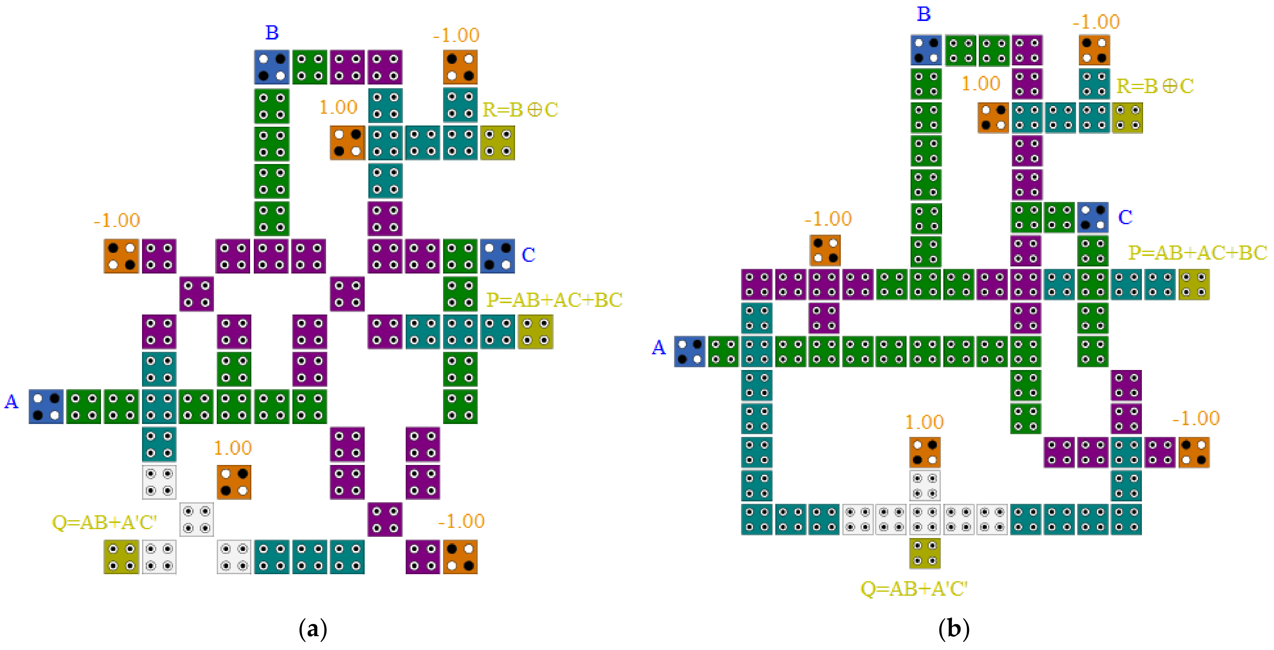
The URG gate also consists of three inputs and three outputs, where A, B, and C are the inputs, and P, Q, and R are the outputs. The URG is another XOR-based reversible gate that can be implemented with two majority and two XOR gates, as presented in Figure 19. The coplanar QCA implementation of URG, without any inverter or crossover, is presented in Figure 20 and Figure 21. Figure 20a shows the first proposed design of this gate, which was implemented based on the circuit illustrated in Figure 20a. A generic QCA majority gate and an XOR gate produced the first output, and a QCA wire produced the second output. In addition, a standard QCA majority gate and an XOR gate were used to make the third output. The simulation results for the proposed URG-a are presented in Figure 20b.
Figure 19.
The URG gate QCA Design.
Figure 20.
(a) QCA layout and (b) simulation results for the proposed URG gate.
Figure 21.
(a) QCA layout and (b) simulation results for the proposed URG gate.
Figure 21a shows the second proposed (URG-b) design of this gate, which was implemented based on the circuit presented in Figure 21a. A rotated QCA majority gate and an XOR gate produced the first output, and a QCA wire produced the second output. In addition, a rotated QCA majority gate and an XOR gate were used to make the third output. The simulation results for the proposed RUG are presented in Figure 21b. The RQCA gate also consists of three inputs and three outputs; this gate, with A, B, and C as inputs, provides P, Q, and R as outputs. The architecture of the RQCA gate is depicted in Figure 22 and is implemented using QCA in Figure 23a,b. We have proposed two new QCA layouts of the RQCA gate (Figure 23a,b). Figure 23a shows the first proposed (proposed-a) design of this gate. The proposed-a RQCA gate was implemented based on the design presented in Figure 23a. A QCA wire and a NOT gate produced the first output, and two XOR gates produced the second output. In addition, an XOR gate and a standard QCA majority gate were used to produce the third output. Figure 23b also shows the second proposed design of this gate. The proposed RQCA-b gate was implemented based on the design presented in Figure 23b. A QCA wire and a NOT gate produced the first output, and two XOR gates produced the second output. In addition, an XOR gate and a rotated QCA majority gate were used to make the third output. The simulations results for the proposed RQCA are presented in Figure 23c. The output delays of both layouts are precisely the same. Therefore, the results of both simulations are the same, and only one of the simulation results is given in Figure 23c. The simulation results in Figure 23c shows a delay of 0.75 clock cycle.
Figure 22.
The RQCA gate QCA Design.
Figure 23.
(a) and (b) QCA layout, and (c) simulation results for the proposed RQCA gate.
Finally, the RQG requires an XOR gate with two majorities and a NOT gate (Figure 24). Its proposed QCA layout is depicted in Figure 25a,b. This gate also consists of three inputs and three outputs, where A, B, and C are the inputs and P, Q, and R are the outputs. We propose two new QCA layouts for RQG gate (Figure 25a,b). Figure 25a shows the first proposed design for this gate, which is implemented based on the circuit presented in Figure 25a. A generic QCA majority gate produced the first output, and a standard QCA majority gate and a NOT gate produced the second output. In addition, an XOR gate was used to make the third output. Figure 25b also shows the dual proposed design for this gate, which was implemented based on the circuit presented in Figure 25b. A rotated QCA majority gate produced the first output, and a rotated QCA majority gate and a NOT gate produced the second output. In addition, an XOR gate was used to make the third output. The circuits comprised 84 cells (Figure 25a) and 84 cells (Figure 25b), and the delay was one clock cycle, according to Figure 25c. The simulation results for the proposed RQG are presented in Figure 25c. Since the output delays of both layouts were the same, the results of both simulations were the same, and only one of the simulation results is given in Figure 25c.
Figure 24.
The RQG gate QCA Design.
Figure 25.
(a) and (b) QCA layout, and (c) simulation results for the proposed RQG gate.
3.2. The Proposed QCA Implementation of Reversible Full Adder\Full Subtractor Circuit
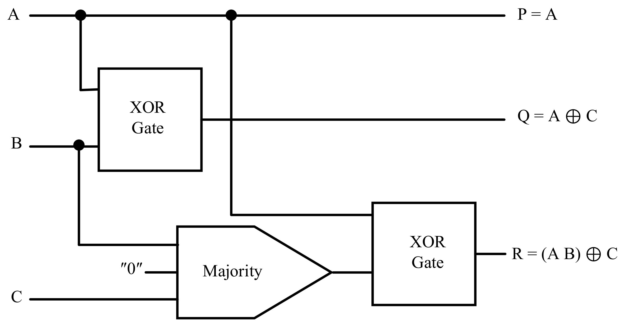
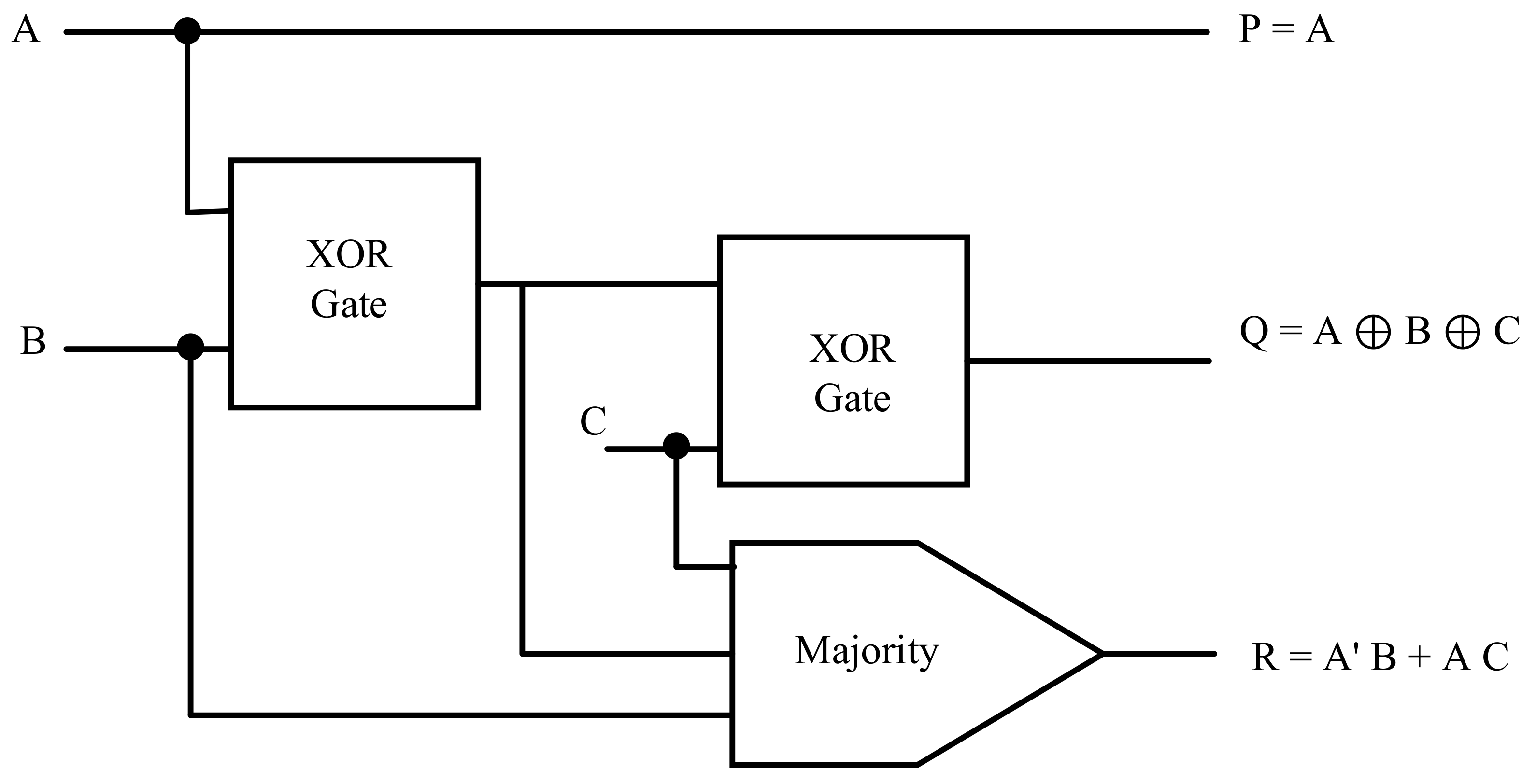
The full-adder\full-subtractor [33] is a combinational circuit that performs addition and subtraction operations. The main advantage of combining FA\FS is sharing logic operations to reduce the required circuit area. It has three inputs (A, B, Cin) and three outputs (S\D, Cout, Bout), according to the truth Table 1) and the following logic equations:
Table 1.
The truth table of full-adder\full-subtractor.
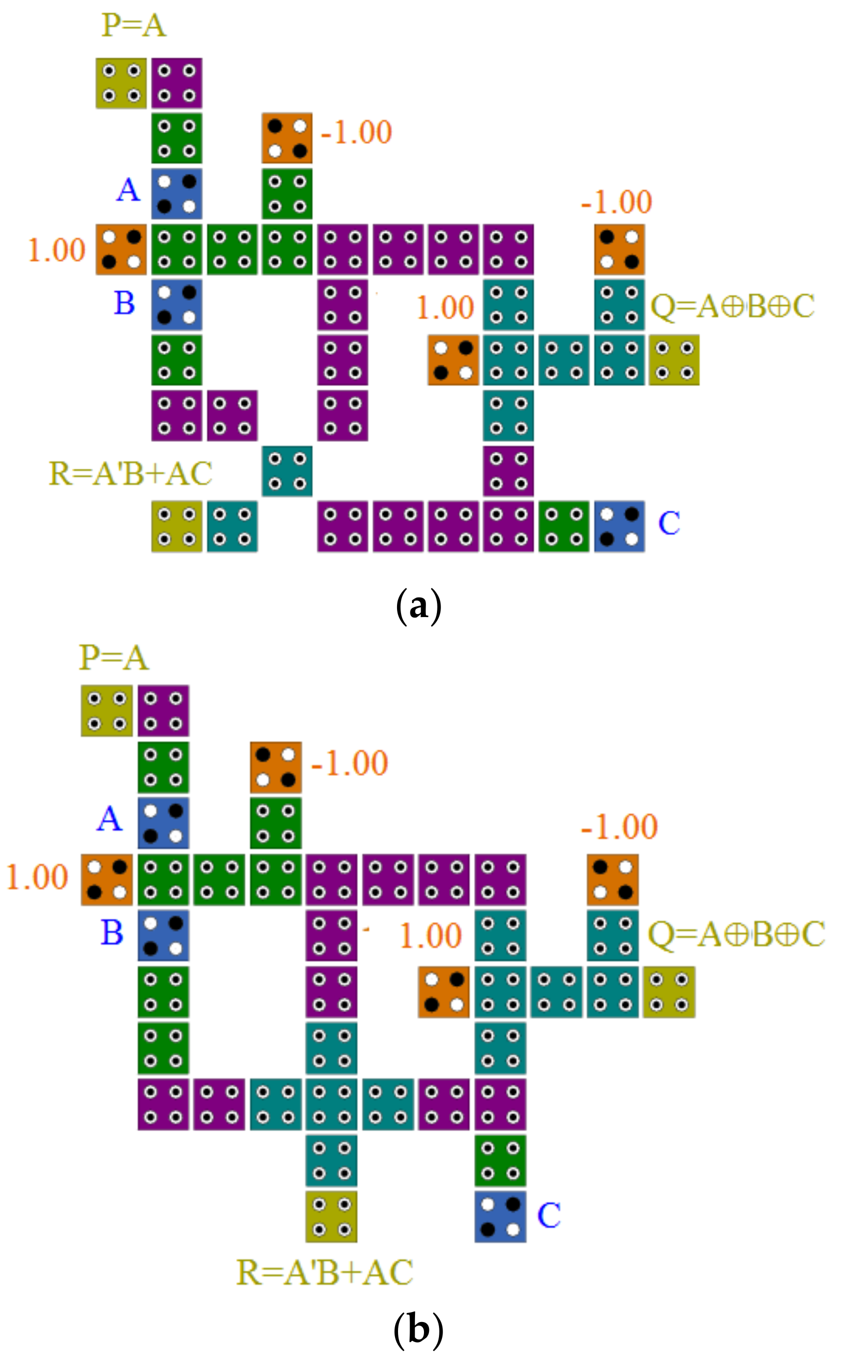
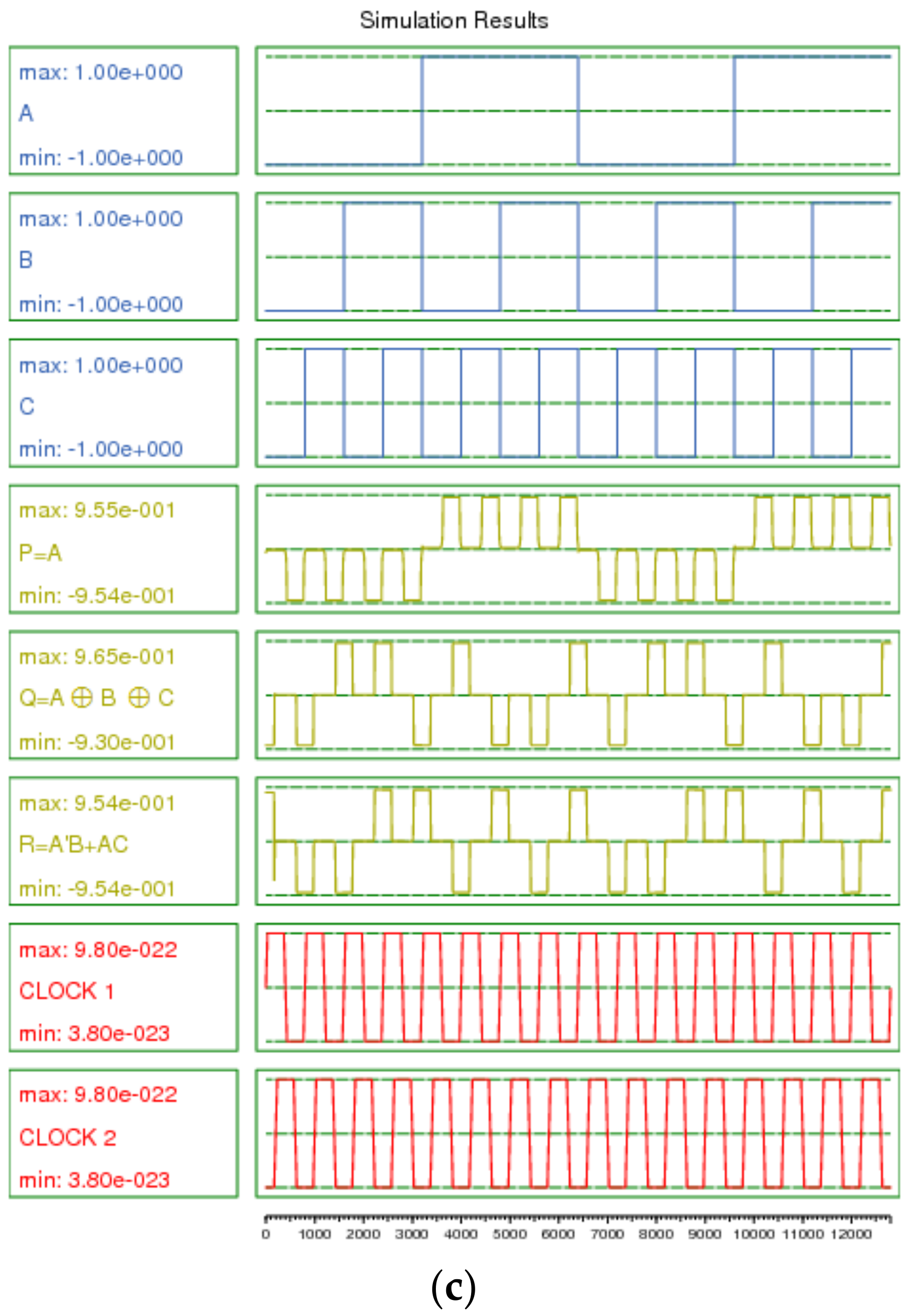
Figure 26 shows the structure of the proposed QCA-based reversible full- adder\full-subtractor circuit. The proposed design includes an RQG reversible gate to produce Cout, Bout, and A⊕B, and a Feynman gate to make A⊕B⊕C together with a garbage output (G). The proposed XOR gate and coplanar wiring have been used to derive a cost-efficient QCA implementation of FA\FS, as shown in Figure 27a,b. The main advantages of these designs, compared with the best state of the art, i.e., [33], are the reduced number of cells and the low area and delay. Furthermore, simulation results in Figure 27c confirm that the delay of the proposed circuits is just five phases, i.e., 1.25 clock cycle.
Figure 26.
The full-adder/full-subtractor QCA Design.
Figure 27.
(a) and (b) QCA layout, and (c) simulation results for the proposed Full Adder\Full Subtractor circuit.
4. Performance Evaluation
This section evaluates the proposed circuits for the QCA implementation of the XOR gate, the other reversible gates and the FA\FS and compares them with the related state-of-the-art works. This evaluation considers the number of cells, the area, and the delay obtained with the QCA Designer tool. The simulation parameters used by the tool are listed in Table 2.
Table 2.
Simulation parameters used on the QCA Designer.
Table 3 compares the remaining proposed reversible gates with the related state-of-the-art. As it can be seen, the comparison was performed among; (i) the proposed Feynman gate and [33,35,36,37,38,39,40,41,42,43,44,45,46,47], (ii) the proposed Toffoli gate and [37,38,39,45,47,48,49,50,51], (iii) the proposed Peres gate and [39,45,47,52,53], (iv) the proposed PQR gate with [25], (v) the proposed TR and [54,55,56], (vi) the proposed RUG gate and [57,58], (vii) the proposed URG gate and [32,59], (viii) the proposed RQCA gate and [31], and (ix) the proposed RQG and [33]. The proposed structures for the reversible gates achieved better performance and efficiency. It is observed in Table 3 that careful cell placement reduces the number of clock phases of the proposed designs for reversible gates Feynman, Toffoli, PQR, RUG, RQCA, and RQG. The same delay is obtained for the others to reduce cell counts or area. These have been obtained in a single layer, leading to a viable fabrication.
Table 3.
Comparison of the proposed design for the reversible gates with the related state of the art.
The evaluation of the proposed FA\FS compared to the related state-of-the-art is shown in Table 4. The proposed-a FA\FS reduction of the consumed area was about 57.14% and 76% in comparison to [33] and [49], and the reduction in the consumed area of the proposed FA\FS-b is about 56.79% and 75.8% in contrast to [33] and [49], respectively. Moreover, for the proposed-a FA\FS, the number of cells was reduced by about 46.05% and 69.17%. In the proposed-b FA\FS, the number of cells was decreased by approximately 46.93% and 69.67%, and the delay for the proposed-a and proposed-b FA\FS was about 28.57% and 37.5% in comparison to [33] and [49], respectively. The reason for achieving the above results is the optimal, cost-effective, and efficient design of the proposed gates and circuits.
Table 4.
Comparison between the suggested FA\FS and the related state of the art.
5. Conclusions
Physical fabrication and mass production are the most critical challenges for implementing QCA circuits based on reversible gates. Most of the available reversible gates designed on QCA technology use multiple layers for crossover, while others require a single layer at the cost of using 45-degree cells. This paper solves both problems by proposing the design of fully single-layer QCA reversible circuits free of 45-degree cells. In addition, an efficient XOR-gate design and several new QCA implementations of the reversible gates were proposed. Finally, as a case study, the proposed reversible gates were used to design a new full adder\full subtractor circuit, which is the basis for obtaining a reversible ALU. We showed that the proposed designs had better performance and efficiency regarding the required cells, area, and delay (number of required clock phases) compared to the related state-of-the-art. The proposed circuits can be implemented in QCA technology which employs reversible logic. Other circuits such as Full Adders, n-bit Adders, Full Subtractors, n-bit Subtractors, and n-bit Adder\Subtractors can be implemented using our proposed reversible gates as the essential elements of the design. Thus, this work proposed cost-effective designs for QCA-based reversible nanoscale computing.
Author Contributions
Conceptualization, M.V.; methodology, M.V.; software, M.V.; validation, M.V., A.N.B., P.L., and A.O.; formal analysis, M.V.; investigation, M.V., A.N.B., P.L., and A.O.; resources, M.V. and A.N.B.; data curation, M.V.; writing—original draft preparation, M.V.; writing—review and editing, A.N.B., P.L., A.O., E.R., and K.A.W.; supervision, A.N.B., P.L., and A.O., E.R. and K.A.W. All authors have read and agreed to the published version of the manuscript.
Funding
This research received no external funding.
Institutional Review Board Statement
Not applicable.
Informed Consent Statement
Not applicable.
Data Availability Statement
Not applicable.
Conflicts of Interest
The authors declare no conflict of interest.
References
- Conte, T.M.; DeBenedictis, E.P.; Gargini, P.A.; Track, E. Rebooting Computing: The Road Ahead. Computer 2017, 50, 20–29. [Google Scholar] [CrossRef]
- DeBenedictis, E.P. Computer Architecture's Changing Role in Rebooting Computing. Computer 2017, 50, 96–99. [Google Scholar] [CrossRef]
- Chang, C.-H.; Molahosseini, A.S.; Zarandi, A.A.E.; Tay, T.F. Residue Number Systems: A New Paradigm to Datapath Optimization for Low-Power and High-Performance Digital Signal Processing Applications. IEEE Circuits Syst. Mag. 2015, 15, 26–44. [Google Scholar] [CrossRef]
- Bennett, C.H. Logical reversibility of computation. IBM J. Res. Dev. 1973, 17, 525–532. [Google Scholar] [CrossRef]
- Chen, A.; Hutchby, J.; Zhirnov, V.; Bourianoff, G. Emerging Nanoelectronic Devices; Chen, A., Hutchby, J., Zhirnov, V., Bourianoff, G., Eds.; John Wiley & Sons Ltd.: Chichester, UK, 2014; ISBN 9781118958254. [Google Scholar]
- DeBenedictis, E.P.; Mee, J.K.; Frank, M.P. The Opportunities and Controversies of Reversible Computing. Computer 2017, 50, 76–80. [Google Scholar] [CrossRef]
- Taha, S.M.R. Reversible Logic Synthesis Methodologies with Application to Quantum Computing; Springer: Berlin, Germany, 2016. [Google Scholar]
- Thapliyal, H.; Ranganathan, N. Reversible Logic-Based Concurrently Testable Latches for Molecular QCA. IEEE Trans. Nanotechnol. 2009, 9, 62–69. [Google Scholar] [CrossRef]
- Roohi, A.; DeMara, R.F.; Khoshavi, N. Design and evaluation of an ultra-area-efficient fault-tolerant QCA full adder. Microelectron. J. 2015, 46, 531–542. [Google Scholar] [CrossRef]
- Liu, W.; O’Neill, M.; Swartzlander, E. Design of Semiconductor QCA Systems; ArTech House Publication: London, UK, 2013. [Google Scholar]
- Macucci, M. Quantum Cellular Automata; Imperial College Press: London, UK, 2006. [Google Scholar]
- Walus, K.; Dysart, T.; Jullien, G.; Budiman, R. QCA Designer: A Rapid Design and Simulation Tool for Quantum-Dot Cellular Automata. IEEE Trans. Nanotechnol. 2004, 3, 26–31. [Google Scholar] [CrossRef]
- Teodosio, T.; Sousa, L. QCA-LG: A tool for the automatic layout generation of QCA combinational circuits. In Proceedings of the IEEE Norchip, Aalborg, Denmark, 19–20 November 2007; pp. 1–5. [Google Scholar] [CrossRef]
- Swartzlander, E.E.; Cho, H.; Kong, I.; Kim, S.-W. Computer arithmetic implemented with QCA: A progress report. In Proceedings of the Forty Fourth Asilomar Conference on Signals, Systems and Computers, Pacific Grove, CA, USA, 7–10 November 2010; pp. 1392–1398. [Google Scholar] [CrossRef]
- Das, J.C.; De, D.; Mondal, S.P.; Ahmadian, A.; Ghaemi, F.; Senu, N. QCA Based Error Detection Circuit for Nano Communication Network. IEEE Access 2019, 7, 67355–67366. [Google Scholar] [CrossRef]
- Shin, S.-H.; Jeon, J.-C.; Yoo, K.-Y. Design of Wire-Crossing Technique Based on Difference of Cell State in Quantum-Dot Cellular Automata. Int. J. Control. Autom. 2014, 7, 153–164. [Google Scholar] [CrossRef]
- Scott, A.; Lewis, T.G. Sustainable computing. Ubiquity 2021, 1–10. [Google Scholar] [CrossRef]
- Landauer, R. Irreversibility and Heat Generation in the Computing Process. IBM J. Res. Dev. 1961, 5, 183–191. [Google Scholar] [CrossRef]
- Denning, P.; Lewis, T. Computers That Can Run Backwards. Am. Sci. 2017, 105, 270. [Google Scholar] [CrossRef]
- Fredkin, E.; Toffoli, T. Conservative logic. Int. J. Theor. Phys. 1982, 21, 219–253. [Google Scholar] [CrossRef]
- Vahabi, M.; Lyakhov, P.; Bahar, A.N.; Wahid, K.A. Design and Implementation of New Coplanar FA Circuits without NOT Gate and Based on Quantum-Dot Cellular Automata Technology. Appl. Sci. 2021, 11, 12157. [Google Scholar] [CrossRef]
- Kianpour, M.; Sabbaghi-Nadooshan, R. Optimized Design of Multiplexor by Quantum-dot Cellular Automata. Int. J. Nanosci. Nanotechnol. 2013, 9, 15–24. [Google Scholar]
- Vahabi, M.; Bahar, A.N.; Otsuki, A.; Wahid, K.A. Ultra-Low-Cost Design of Ripple Carry Adder to Design Nanoelectronics in QCA Nanotechnology. Electronics 2022, 11, 2320. [Google Scholar] [CrossRef]
- Vahabi, M.; Lyakhov, P.; Bahar, A.N. Design and Implementation of Novel Efficient Full Adder/Subtractor Circuits Based on Quantum-Dot Cellular Automata Technology. Appl. Sci. 2021, 11, 8717. [Google Scholar] [CrossRef]
- Chabi, A.M.; Roohi, A.; Khademolhosseini, H.; Sheikhfaal, S.; Angizi, S.; Navi, K.; DeMara, R.F. Towards ultra-efficient QCA reversible circuits. Microprocess. Microsyst. 2017, 49, 127–138. [Google Scholar] [CrossRef]
- Feynman, R. Quantum Mechanical Computers. Opt. News 1985, 11, 11–20. [Google Scholar] [CrossRef]
- Toffoli, T. Reversible computing. In International Colloquium on Automata, Languages, and Programming; Springer: Berlin/Heidelberg, Germany, 1980; pp. 632–644. [Google Scholar]
- Peres, A. Reversible logic and quantum computers. Phys. Rev. A 1985, 32, 3266–3276. [Google Scholar] [CrossRef] [PubMed]
- Saravanan, S.; Vennila, I.; Mohanram, S. Design and Implementation of an Efficient Reversible Comparator Using TR Gate. Circuits Syst. 2016, 07, 2578–2592. [Google Scholar] [CrossRef]
- Sen, B.; Adak, T.; Anand, A.S.; Sikdar, B.K. Synthesis of reversible universal QCA gate structure for energy efficient digital design. In Proceedings of the IEEE Region 10 Conference TENCON, Bali, Indonesia, 21–24 November 2011; pp. 806–810. [Google Scholar] [CrossRef]
- Sen, B.; Dutta, M.; Some, S.; Sikdar, B.K. Realizing Reversible Computing in QCA Framework Resulting in Efficient Design of Testable ALU. ACM J. Emerg. Technol. Comput. Syst. 2014, 11, 1–22. [Google Scholar] [CrossRef]
- Islam, M.S.; Abdullah-Al-Shafi, M.; Bahar, A.N. A new approach of presenting universal reversible gate in nanoscale. Int. J. Comput. Appl. 2016, 134, 1–4. [Google Scholar]
- Taherkhani, E.; Moaiyeri, M.H.; Angizi, S. Design of an ultra-efficient reversible full adder-subtractor in quantum-dot cellular automata. Optik 2017, 142, 557–563. [Google Scholar] [CrossRef]
- Chen, H.; Lv, H.; Zhang, Z.; Cheng, X.; Xie, G. Design and Analysis of a Novel Low-Power Exclusive-OR Gate Based on Quantum-Dot Cellular Automata. J. Circuits Syst. Comput. 2019, 28, 1950141. [Google Scholar] [CrossRef]
- Karkaj, E.T.; Heikalabad, S.R. Binary to gray and gray to binary converter in quantum-dot cellular automata. Optik 2017, 130, 981–989. [Google Scholar] [CrossRef]
- Vahabi, M.; Lyakhov, P.; Bahar, A.N.; Otsuki, A.; Wahid, K.A. Novel Reversible Comparator Design in Quantum Dot-Cellular Automata with Power Dissipation Analysis. Appl. Sci. 2022, 12, 7846. [Google Scholar] [CrossRef]
- Kumar, P.; Singh, S. Optimization of the area efficiency and robustness of a QCA-based reversible full adder. J. Comput. Electron. 2019, 18, 1478–1489. [Google Scholar] [CrossRef]
- Ahmed, S.; Naz, S.F.; Sharma, S. Quantum dot Cellular Automata based Fault Tolerant Fingerprint Authentication Systems using Reversible Logic Gates. GAZI Univ. J. Sci. 2021, 35, 586–604. [Google Scholar] [CrossRef]
- Das, J.C.; De, D. Computational fidelity in reversible quantum-dot cellular automata channel routing under thermal randomness. Nano Commun. Netw. 2018, 18, 17–26. [Google Scholar] [CrossRef]
- Bahar, A.N.; Ahmad, F.; Nahid, N.M.; Hassan, K.; Al Shafi, A.; Ahmed, K. An optimal design of conservative efficient reversible parity logic circuits using QCA. Int. J. Inf. Technol. 2018, 11, 785–794. [Google Scholar] [CrossRef]
- Das, J.C.; De, D. Feynman gate based design of n-bit reversible inverter and its implementation on quantum-dot cellular automata. Nano Commun. Netw. 2020, 24, 100298. [Google Scholar] [CrossRef]
- Seyedi, S.; Otsuki, A.; Navimipour, N. A New Cost-Efficient Design of a Reversible Gate Based on a Nano-Scale Quantum-Dot Cellular Automata Technology. Electronics 2021, 10, 1806. [Google Scholar] [CrossRef]
- Patidar, M.; Gupta, N. An ultra-efficient design and optimized energy dissipation of reversible computing circuits in QCA technology using zone partitioning method. Int. J. Inf. Technol. 2021, 14, 1483–1493. [Google Scholar] [CrossRef]
- Debnath, B.; Das, J.C.; De, D.; Ghaemi, F.; Ahmadian, A.; Senu, N. Reversible Palm Vein Authenticator Design with Quantum Dot Cellular Automata for Information Security in Nanocommunication Network. IEEE Access 2020, 8, 174821–174832. [Google Scholar] [CrossRef]
- Roy, A.; Singh, A.D.; Saha, A.; Saha, S.; Gupta, V.; Qingyi, Z.; Bhattacharya, S.; Bhattacharjee, S. A Novel Design of Reversible Gate using Quantum-Dot Cellular Automata (QCA). In Proceedings of the 2020 IEEE 1st International Conference for Convergence in Engineering (ICCE), Kolkata, India, 5–6 September 2020; pp. 110–115. [Google Scholar]
- Mukherjee, C.; Panda, S.; Mukhopadhyay, A.K.; Maji, B. Utilization of LTEx Feynman Gate in Designing the QCA Based Reversible Binary to Gray and Gray to Binary Code Converters. Micro Nanosyst. 2020, 12, 187–200. [Google Scholar] [CrossRef]
- Sasamal, T.N.; Singh, A.K.; Ghanekar, U. Toward Efficient Design of Reversible Logic Gates in Quantum-Dot Cellular Automata with Power Dissipation Analysis. Int. J. Theor. Phys. 2017, 57, 1167–1185. [Google Scholar] [CrossRef]
- Iqbal, J.; Banday, M.T. Applications of Toffoli Gate for designing the classical gates using quantum-dot cellular automata. Int. J. Recent Sci. Res. 2015, 6, 7764–7769. [Google Scholar]
- Kianpour, M.; Sabbaghi-Nadooshan, R. Novel 8-bit reversible full adder/subtractor using a QCA reversible gate. J. Comput. Electron. 2017, 16, 459–472. [Google Scholar] [CrossRef]
- Bhoi, B.K.; Misra, N.K.; Pradhan, M. Analysis on Fault Mapping of Reversible Gates with Extended Hardware Description Language for Quantum Dot Cellular Automata Approach. Sens. Lett. 2019, 17, 371–378. [Google Scholar] [CrossRef]
- Safoev, N.; Abdukhalil, G.; Abdisalomovich, K.A. QCA based Priority Encoder using Toffoli gate. In Proceedings of the 2020 IEEE 14th International Conference on Application of Information and Communication Technologies (AICT), Tashkent, Uzbekistan, 7–9 October 2020; pp. 1–4. [Google Scholar]
- Reshi, J.I.; Banday, M.T. Realization of Peres gate as universal structure using quantum Dot cellular automata. J. Nanosci. Technol. 2016, 2, 115–118. [Google Scholar]
- Das, J.C.; De, D. Novel low power reversible binary incrementer design using quantum-dot cellular automata. Microprocess. Microsyst. 2016, 42, 10–23. [Google Scholar] [CrossRef]
- Das, J.C.; De, D. Reversible Comparator Design Using Quantum Dot-Cellular Automata. IETE J. Res. 2015, 62, 323–330. [Google Scholar] [CrossRef]
- Bahar, A.N.; Waheed, S.; Hossain, N.; Bahar, A.N. A new approach of presenting reversible logic gate in nanoscale. Springerplus 2015, 4, 1–7. [Google Scholar] [CrossRef] [PubMed]
- Sarma, R.; Jain, R. Quantum Gate Implementation of a Novel Reversible Half Adder and Subtractor Circuit. In Proceedings of the 2018 International Conference on Intelligent Circuits and Systems (ICICS), Phagwara, India, 20–21 April 2018; pp. 72–76. [Google Scholar] [CrossRef]
- Das, J.C.; De, D. Optimized Design of Reversible Gates in Quantum Dot-Cellular Automata: A Review. Rev. Theor. Sci. 2016, 4, 279–286. [Google Scholar] [CrossRef]
- Sasamal, T.N.; Mohan, A.; Singh, A.K. Efficient Design of Reversible Logic ALU Using Coplanar Quantum-Dot Cellular Automata. J. Circuits Syst. Comput. 2017, 27, 1850021. [Google Scholar] [CrossRef]
- Al-Shafi, A.; Aneek, R.H.; Bahar, A.N. Universal Reversible Gate in Quantum-Dot Cellular Automata (QCA): A Multilayer Design Paradigm. Int. J. Grid Distrib. Comput. 2017, 10, 43–50. [Google Scholar] [CrossRef]
- Ahmad, F.; Ahmed, S.; Kakkar, V.; Bhat, G.M.; Bahar, A.N.; Wani, S. Modular Design of Ultra-Efficient Reversible Full Adder-Subtractor in QCA with Power Dissipation Analysis. Int. J. Theor. Phys. 2018, 57, 2863–2880. [Google Scholar] [CrossRef]
- Hashemi, S.; Azghadi, M.R.; Navi, K. Design and analysis of efficient QCA reversible adders. J. Supercomput. 2018, 75, 2106–2125. [Google Scholar] [CrossRef]
Disclaimer/Publisher’s Note: The statements, opinions and data contained in all publications are solely those of the individual author(s) and contributor(s) and not of MDPI and/or the editor(s). MDPI and/or the editor(s) disclaim responsibility for any injury to people or property resulting from any ideas, methods, instructions or products referred to in the content. |
© 2023 by the authors. Licensee MDPI, Basel, Switzerland. This article is an open access article distributed under the terms and conditions of the Creative Commons Attribution (CC BY) license (https://creativecommons.org/licenses/by/4.0/).